

Page 1

WARNING
Do not use solder containing lead.
This product has been manufactured using lead-free solder in
order to help preserve the environment.
Because of this, be sure to use lead-free solder when carrying
out repair work, and never use solder containing lead.
Lead-free solder has a melting point that is 30 - 40°C (86 104°F) higher than solder containing lead, and moreover it does
not contain lead which attaches easily to other metals. As a
result, it does not melt as easily as solder containing lead, and
soldering will be more difficult even if the temperature of the
soldering iron is increased.
The extra difficulty in soldering means that soldering time will
increase and damage to the components or the circuit board
may easily occur.
Because of this, you should use a soldering iron and solder
that satisfy the following conditions when carrying out repair
work.
Soldering iron
Use a soldering iron which is 70 W or equivalent, and which
lets you adjust the tip temperature up to 450°C (842°F). It
should also have as good temperature recovery characteristics as possible.
Set the temperature to 350°C (662°F) or less for chip components, to 380°C (716°F) for lead wires and similar, and to 420°C
(788°F) when installing and removing shield plates.
The tip of the soldering iron should have a C-cut shape or a
driver shape so that it can contact the circuit board as flat or in
a line as much as possible.
Note:
If replacing existing solder containing lead with lead-free solder in the soldered parts of products that have been manufactured up until now, remove all of the existing solder at those
parts before applying the lead-free solder.
Solder
Use solder with the metal content and composition ratio by
weight given in the table below. Do not use solders which do
not meet these conditions.
Metal content
Composition
ratio by weight
Lead-free solder is available for purchase as a service tool.
Use the following part number when ordering:
Part name: Lead-free solder with resin (0.5 mm dia., 500 g)
Part number: VJ8-0270
Tin (Sn) Silver (Ag)
96.5 %
3.0 %
Copper (Cu)
0.5 %
– 2 –
Page 2
1. OUTLINE OF CIRCUIT DESCRIPTION
1-1. CCD CIRCUIT DESCRIPTION
1. IC Configuration
The CCD peripheral circuit block basically consists of the following ICs.
IC901 (MN39727PMJ-A) CCD imager
IC932 (AN20111A) V driver
IC931 (AD9942BBCZ) CDS, AGC, A/D converter,
H driver, vertical TG
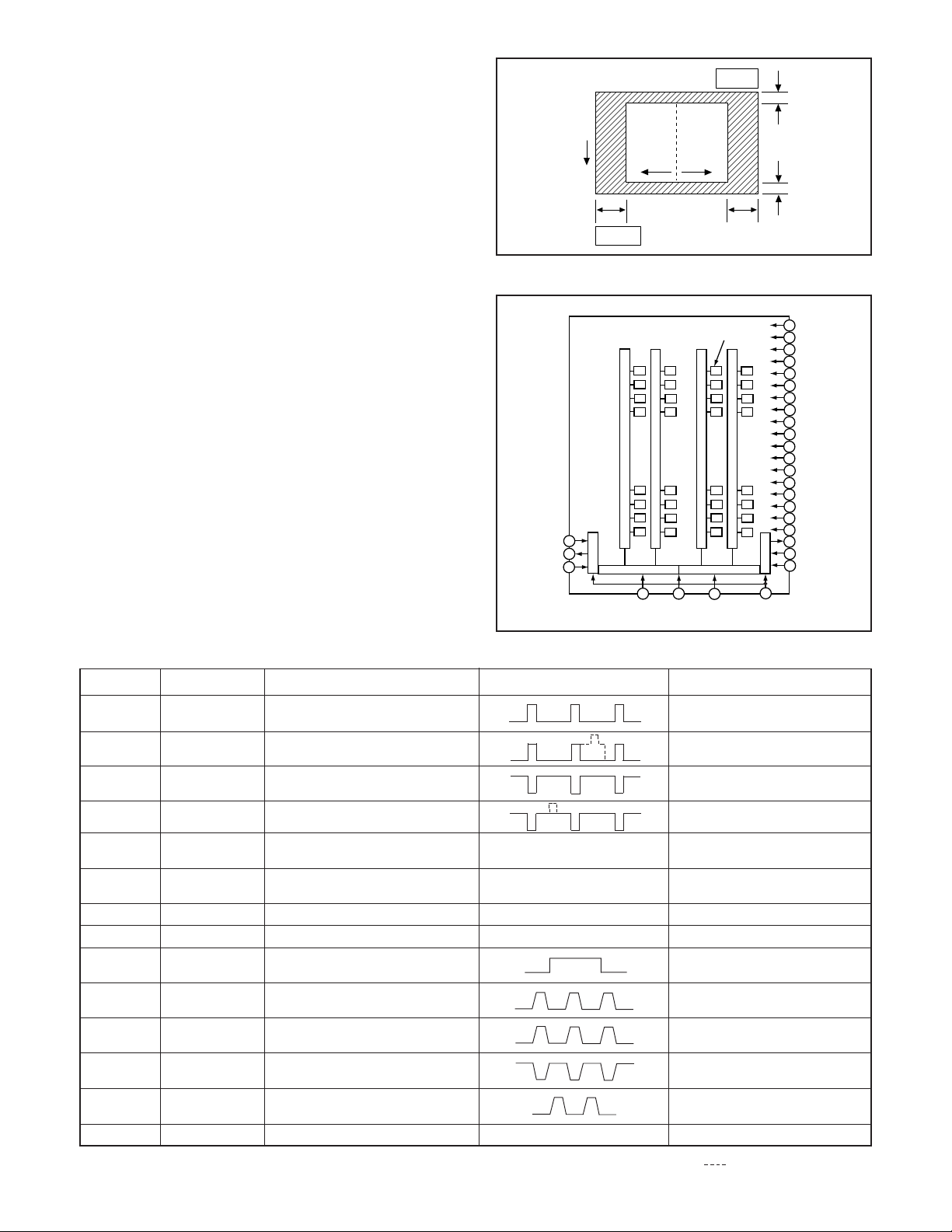
Pin 1
6
V
H
58
H
6
58
Pin 15
2. IC901 (CCD)
[Structure]
1/2.5 inch positive pixel-type color frame-reading fixed picture elements
2 channel output
Optical size 1/2.5 type format
Effective pixels 2612 (H) X 1954 (V)
Pixels in total 2728 (H) X 1966 (V)
Optical black
Horizontal (H) direction: Front 58 pixels, Rear 0 pixels
Vertical (V) direction: Front 6 pixels, Rear 6 pixels
Dummy bit number Horizontal : 28 Vertical :5
Pin No.
1, 2, 7, 8,
10, 11, 20
Symbol Pin Description
1B, V2, V3B, V4,
V
V7B, V7R, V8
Vertical register transfer clock
Fig. 1-1.Optical Black Location (Top View)
Output part 2
24
R
ø
1
2
3
4
5
6
7
8
9
10
11
12
19
20
14
18
25
13
27
28
26
VO1
VDD1
GND1
16
15
17
Horizontal shift register 1
Output part 1
21
HL
ø
Photo diode
Vertical shift register
Horizontal shift register 2
22
23
H2
H1
ø
ø
Fig. 1-2. CCD Block Diagram
Waveform
Voltag e
-6.0 V, 0 V
ø
V8
ø
V7B
ø
V7A
ø
V6
ø
V5B
ø
V5A
ø
V4
ø
V3B
ø
V3A
ø
V2
ø
V1B
ø
V1A
ø
V5R
ø
V7R
SUB
SUBSW
PT
GND
VO2
VDD2
GND2
3, 9, 12
4, 5, 19
6
13, 17, 26
14
15, 28
16, 27
18
21
22
23
25
1A, V3A, V7A Vertical register transfer clock
V
V5B, V5R, V6
5A
V
GND, GND1,
GND2
SUB
Vertical register transfer clock
Vertical register transfer clock
GND
Substrate clock
Circuit power
VOL1, VOL2
Signal output
Substrate controlSUB SW
HL
H
H
R
PT
1
2
Horizontal register transfer clock
Horizontal register transfer clock
Horizontal register transfer clock
Reset gate clock24
Protection transister bias
Table 1-1. CCD Pin Description
– 3 –
-6.0 V, 0 V, 12 V
-6.0 V, 0 V
-6.0 V, 0 V, 12 V
GND
DC
DC
0 V
Aprox. 6 V
(Different from every CCD)
12 VVDD1, VDD2
DC Aprox. 12 V
0, 3.4 V (When importing all
picture element: 3.4 V)
0 V, 3.4 V
0 V, 3.4 V
0 V, 3.4 V
4.2 V, 9.0 V
DC
-6 V
When sensor read-out
Page 3
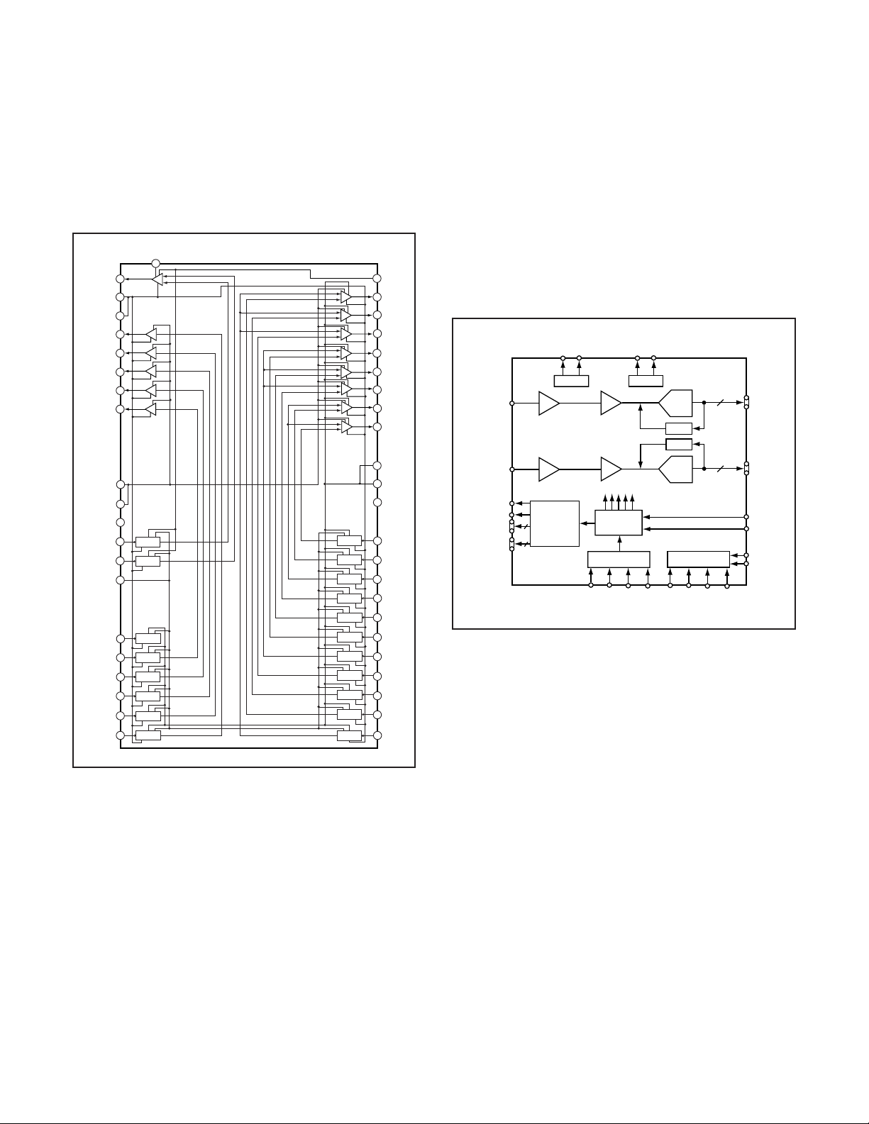
3. IC932 (V Driver)
A V driver (IC932) is necessary in order to generate the clocks
(vertical transfer clock and electronic shutter clock) which
driver the CCD.
In addition the XV1-XV8 signals which are output from IC102
are vertical transfer clocks, and the XSG signal is superimposed onto XV1, XV3, XV5 and XV7 at IC932 in order to generate a ternary pulse. In addition, the XSUB signal which is
output from IC102 is used as the sweep pulse for the electronic shutter.
VMSUB
13
OSUB
OV5R
OV7R
OV4
OV6
OV8
VM
RESET
SUBCNT
SUB
VDC
V7R
V5R
3-level
14
8
VL
41
VL
2-level
26
2-level
25
2-level
31
2-level
30
2-level
29
12
VM
37
43
Level
4
conversion
Level
5
conversion
6
Level
50
V8
conversion
Level
V6
46
conversion
Level
45
V4
conversion
Level
44
V2
conversion
Level
55
conversion
Level
54
conversion
3-level
3-level
3-level
3-level
3-level
3-level
3-level
3-level
Level
conversion
Level
conversion
Level
conversion
Level
conversion
Level
conversion
Level
conversion
Level
conversion
Level
conversion
Level
conversion
Level
conversion
Level
conversion
11
VHH
27
OV1B
28
OV1A
OV3B
22
23
OV3A
20
OV5B
21
OV5A
15
OV7B
19
OV7A
10
VH
38
VH
7
GND
62
CH8
63
CH4
3
V7
59
CH7
60
CH3
61
V5
56
CH6
57
CH2
V3
58
52
CH1
53
V1
4. IC931 (H Driver, CDS, AGC and A/D converter)
IC931 contains the functions of H driver, CDS, AGC and A/D
converter. As horizontal clock driver for CCD image sensor,
HØ1, HØ2, HØL and RG are generated inside, and output to
CCD.
The video signal which is output from the CCD is input to pin
(1) and pin (74) of IC931. There are sampling hold blocks
generated from the SHP and SHD pulses, and it is here that
CDS (correlated double sampling) is carried out.
After passing through the CDS circuit, the signal passes
through the AGC amplifier (VGA: Variable Gain Amplifier). It
is A/D converted internally into a 14-bit signal, and is then
input to MOVIC (IC102). The gain of the VGA amplifier is controlled by pins (4), (5), (6), (69), (70) and (71) serial signal
which is output from ASIC (IC101).
REFT_B
TIMING
CORE
SYNC
HD_B
REFB_B
VREF_B
VD_B
ADC
CLAMP
CLAMP
ADC
SL_A
SDATA_A
AD9942
INTERNAL
REGISTERS
SL_B
14
14
SDATA_B
DOUT_A
DOUT_B
CLI_A
CLI_B
SCK_A
SCK_B
CCDIN_A
CCDIN_B
RG_A
RG_B
H1A TO H4A
H1B TO H4B
REFT_A
REFB_A
VREF_A
CDS
CDS
4
HORIZONTAL
DRIVERS
4
VGA
0~18 dB
0~18 dB
VGA
INTERNAL CLOCKS
PRECISION
GENERATOR
VD_A
HD_A
Fig. 1-4. IC931 Block Diagram
Fig. 1-3. IC932 Block Diagram
– 4 –
Page 4

1-2. CP1 and VF1 CIRCUIT DESCRIPTION
1. Circuit Description
1-1. Digital clamp
The optical black section of the CCD extracts averaged values
from the subsequent data to make the black level of the CCD
output data uniform for each line. The optical black section of
the CCD averaged value for each line is taken as the sum of
the value for the previous line multiplied by the coefficient k
and the value for the current line multiplied by the coefficient
1-k.
1-2. Signal processor
1. γ correction circuit
This circuit performs (gamma) correction in order to maintain
a linear relationship between the light input to the camera and
the light output from the picture screen.
2. Color generation circuit
This circuit converts the CCD data into RGB signals.
3. Matrix circuit
This circuit generates the Y signals, R-Y signals and B-Y signals from the RGB signals.
4. Horizontal and vertical aperture circuit
This circuit is used gemerate the aperture signal.
1-3. AE/AWB and AF computing circuit
The AE/AWB carries out computation based on a 64-segment
screen, and the AF carries out computations based on a 6segment screen.
1-4. SDRAM controller
This circuit outputs address, RAS, CAS and AS data for controlling the SDRAM. It also refreshes the SDRAM.
1-5. Communication control
1. SIO
This is the interface for the 8-bit microprocessor.
2. PIO/PWM/SIO for LCD
8-bit parallel input and output makes it possible to switch between individual input/output and PWM input/output.
2. Outline of Operation
When the shutter opens, the reset signals (ASIC and CPU)
and the serial signals (“take a picture” commands) from the 8bit microprocessor are input and operation starts. When the
TG/SG drives the CCD, picture data passes through the A/D
and CDS, and is then input to the MOVIC as 13-bit 2 channels
data. The data that is input to the MOVIC is converted to 1 ch
from 2 ch, and input to the SDRAM through digital clamp.
The data that is input to SDRAM is input to the ASIC through
the D1 I/F. The AF, AE, AWB, shutter, and AGC value are computed from this data, and three exposures are made to obtain
the optimum picture. The data which has already been stored
in the SDRAM is read by the CPU and color generation is carried out. Each pixel is interpolated from the surrounding data
as being either R, G, and B primary color data to produce R, G
and B data. At this time, correction of the lens distortion which
is a characteristic of wide-angle lenses is carried out. After
AWB and γ processing are carried out, a matrix is generated
and aperture correction is carried out for the Y signal, and the
data is then compressed by JPEG and is then written to card
memory (SD card).
When the data is to be output to an external device, it is taken
data from the memory and output via the USB I/F. When played
back on the LCD and monitor, data is transferred from memery
to the SDRAM, and the image is then elongated so that it is
displayed over the SDRAM display area.
3. LCD Block
The LCD display circuit is located on the CP1 board, and
consists of components such as a power circuit.
The signals from the ASIC are 8-bit digital signals, that is
input to the LCD directly. The 8-bit digital signals are converted to RGB signals inside the LCD driver circuit . This LCD
has a 3-wire serial, and functions such as the brightness and
image quality are controlled.
Because the LCD closes more as the difference in potential
between the VCOM (common polar voltage: AC) and the R,
G and B signals becomes greater, the display becomes darker;
if the difference in potential is smaller, the element opens and
the LCD become brighter.
In addition, the timing pulses for signals other than the video
signals are also input from the ASIC directory to the LCD.
1-6. TG/SG
Timing generated for 5 million pixel horizontal addtion CCD
control.
1-7. Digital encorder
It generates chroma signal from color difference signal.
– 5 –
Page 5

4. Lens drive block
4-1. Focus drive
The 16-bit serial data signals (LENS_SD) and (LENS_CK and
LENS_EN) which are output from the ASIC (IC101) are used
to drive (FOCUS A +, FOCUS A -, FOCUS B + and FOCUS B
-) by the motor driver (IC951), and are then used to microstepdrive the stepping motor for focusing operation. Detection of
the standard focusing positions is carried out by means of the
photointerruptor (F_SENSE) inside the lens block.
4-2. Zoom drive
The 16-bit serial data signals (LENS_SD) and (LENS_CK and
LENS_EN) which are output from the ASIC (IC101) are used
to drive (ZOOM A +, ZOOM A -, ZOOM B + and ZOOM B -) by
the motor driver (IC951), and are then used to microstep-drive
the stepping motor for zooming operation. Detection of the standard zooming positions is carried out by means of the
photointerruptor (Z_SENSE) inside the lens block.
4-3. ND filter
The ND filter drive signals (NDON and NDOFF) which are output from the ASIC (IC101) are used to drive (ND + and ND -)
by the motor driver (IC951), and then the ND filter is inserted
into and removed from the beam path.
5. Video Clip Recording and Playback
5-1. Recording
The signal from the camera block is input to IC102 (MOVIC).
The data that is input to the MOVIC is input to SDRAM, and
input to IC101 (ASIC) through D1 (I/F).
The MOVIC converts this data to encoded MPEG4 data, after
which it is returned to the ASIC as streaming data, and the
data is then written in sequence onto the SD card. At this time,
the audio signals that are input to the built-in microphone are
converted into digital data by the audio CODEC IC of IC183,
and they are then input to IC102 (MOVIC). The audio data is
then encoded (AAC) by IC102, and then it is returned to the
ASIC as streaming data and is then written in sequence onto
the SD card together with the image signals described above.
5-2. Playback
The data is read from the SD card and input to IC102 as streaming data. The encoded data is decoded into image data by
IC102 and then returned to the ASIC where it is displayed by
the LCD or on a TV monitor. D4 image is output from IC102. At
this time, the audio data is also decoded by IC102, and is input
to IC183 as digital data. D/A conversion is carried out at IC183,
and the sound is then output to the speaker or to the LINE
OUT terminal.
4-4. Iris drive
The drive method is a galvanometer type without braking coil.
The output from the Hall sensor inside the lens is amplified by
the Hall amplifier circuit inside the IC971 lens drive IC, and the
difference between the current and target aperture determined
by the resulting output and the exposure amout output from
the ASIC (IC101) is input to the servo amplifier circuit (IC971)
to keep the aperture automatically controlled to the target aperture. The lens aperture control signal is output from IC971
and is input to lens drive IN6B of IC951. IC951 functions as
the driver for driving the lens.
4-5. Shutter drive
Reverse voltage is applied to the above aperture drive coil to
operate the shutter. When the shutter operates, the OC_EN
and OC_CONT signals are maintained at a high level, it is
input to IN6B of IC951 with low level.
At the same time the SHUTTER + signal that is output from
the ASIC (IC101) becomes high (input to IN6A of IC951) and
the shutter operates. IC951 functions as the driver for driving
the lens.
6. Audio CODEC Circuit (IC183)
The audio signals from the microphone are converted into 16bit digital data. AD conversion is carried out at a maximum
sampling frequency of 48 kHz.
During audio playback, the 16-bit digital data is converted into
analog signals and these drive the speaker or line out system.
DA conversion is carried out at a maximum sampling frequency
of 48 kHz.
– 6 –
Page 6

1-3. PW1 POWER CIRCUIT DESCRIPTION
1. Outline
This is the main power circuit, and is comprised of the following blocks.
Switching controller (IC501)
Analog 12 V power output (L5009)
Analog -6 V power output (L5008)
Analog 3.4 V power output (L5013)
5 V power output (L5005)
Digital 3.25 V power output (L5006)
Digital 1.2 V power output (L5007)
Backlight power output (L5011)
2. Switching Controller (IC501)
This is the basic circuit which is necessary for controlling the
power supply for a PWM-type switching regulator, and is provided with eight built-in channels, only SU (5 V), M (digital
3.25 V), SD (digital 1.2 V), BST (analog 12 V), INV (analog -6
V), AFE (analog 3.4 V) and LED (backlight) are used.
Each power supply output is received, and the PWM duty is
varied so that each one is maintained at the correct voltage
setting level.
Feedback for the backlight power (LED) is provided to the
both ends voltage of registance so that regular current can
be controlled to be current that was setting.
3. Analog 12 V Power Output
HVVDD is output through +12 V (A) and IC503 regulator. Feedback for the +12 V (A) is provided to the switching controller
(Pin (26) of IC501) so that PWM control can be carried out.
4. Analog -6 V Power Output
-6 V (A) is output. Feedback for the -6 V (A) is provided to the
swiching controller (Pin (25) of IC501) so that PWM control
can be carried out.
5. Analog 3.4 V Power Output
+3.4 V (A) is output. Feedback for the +3.4 V (A) is provided
to the switching controller (Pin (11) of IC501) so that PWM
control to be carried out.
6. 5 V Power Output
+5 V is output. Feedback for the +5 V is provided to the switching controller (Pin (42) of IC501) so that PWM control to be
carried out.
7. Digital 3.25 V Power Output
+3.25 V (D) is output. Feedback for the +3.25 V (D) is provided to the switching controller (Pin (2) of IC501) so that
PWM control to be carried out.
2-1. Short-circuit protection circuit
If output is short-circuited for the length of time determined
by internal fixing of IC501 , all output is turned off. The control
signal (P ON) are recontrolled to restore output.
8. Digital 1.2 V Power Output
+1.2 V (D) is output. Feedback for the +1.2 V (D) is provided
to the switching controller (Pin (12) of IC501) so that PWM
control to be carried out.
9. Backlight Power Supply output
Regular current is being transmitted to LED for LCD backlight. Feedback for the both ends voltage of registance that is
being positioned to in series LED are provided to the switching controller (Pin (37) of IC501) so that PWM control to be
carried out.
10. Camera charging circuit
If the camera’s power is turned off, play mode and USB connection mode (card reader and pictbridge) setting while it is
connected to the AC adaptor, the battery will be recharged. In
the above condition, a CTL signal is sent from the microprocessor and recharging starts.
– 7 –
Page 7

1-4. PW1 STROBE CIRCUIT DESCRIPTION
1. Charging Circuit
When UNREG power is supplied to the charge circuit and the
CHG signal from microprocessor becomes High (3.3 V), the
charging circuit starts operating and the main electorolytic
capacitor is charged with high-voltage direct current.
However, when the CHG signal is Low (0 V), the charging
circuit does not operate.
1-1. Charge switch
When the CHG signal switches to Hi, IC541 starts charging
operation.
1-2. Power supply filter
C5401 constitutes the power supply filter. They smooth out
ripples in the current which accompany the switching of the
oscillation transformer.
1-3. Oscillation circuit
This circuit generates an AC voltage (pulse) in order to increase the UNREG power supply voltage when drops in current occur. This circuit generates a drive pulse with a frequency
of approximately 200-300 kHz.
2. Light Emission Circuit
When FLCLT signal is input from the ASIC, the stroboscope
emits light.
2-1. Emission control circuit
When the FLCLT signal is input to the emission control circuit, Q5402 switches on and preparation is made to the light
emitting. Moreover, when a FLCLT signal becomes Lo, the
stroboscope stops emitting light.
2-2. Trigger circuit
The Q5402 is turned ON by the FLCLT signal and light emission preparation is preformed. Simultaneously, high voltage
pulses of several kV are emitted from the trigger coil and applied to the light emitter.
2-3. Light emitting element
When the high-voltage pulse form the trigger circuit is applied to the light emitting part, currnet flows to the light emitting element and light is emitted.
Beware of electric shocks.
1-4. Oscillation transformer
The low-voltage alternating current which is generated by the
oscillation control circuit is converted to a high-voltage alternating current by the oscillation transformer.
1-5. Rectifier circuit
The high-voltage alternating current which is generated at
the secondary side of T5401 is rectified to produce a highvoltage direct current and is accumulated at electrolytic capacitor C5412.
1-6. Charge monitoring circuit
The functions programmed in the IC541 monitor oscillations
and estimate the charging voltage. If the voltage exceeds the
rated value, charging automatically stops. Then, the
ZCHGDONE signal is changed to Lo output and a "charging
stopped" signal is sent to the microcomputer.
– 8 –
Page 8

1-5. SYA CIRCUIT DESCRIPTION
1. Configuration and Functions
For the overall configuration of the SYA block, refer to the block diagram. The SYA block centers around a 8-bit microprocessor
(IC301), and controls camera system condition (mode).
The 8-bit microprocessor handles the following functions.
1. Operation key input, 2. Clock control and backup, 3. Power ON/OFF, 4. Storobe charge control.
Pin
1
2
3
4
5
6
7
8
9
10
11
12
13
14
15
16
17
18
19
20
21 CAM_LED
22 BAT_LED
23 PLLEN
24
25 TH_ON
26
27
28
29
30~33
34
35, 36
37
38
39
40
41
42
43~46
47
48
49
Signal
SCLK
ZCARD
BACKUP CTL
CHG_CNT
HOT LINE
VF. LED (R)
LCD PWM
NOT USED
VDD2
VSS2
CHG ON
LCD ON1
CLKSEL0
P ON
BL ON
LENS 4M
NOT USED
MRST
VF. LED (G)
ZUSB_DET
USB_TRIG
BATCHGERR
LCD ON2
BATCHGCNT
AVREF ON
SCAN IN5~2
NOT USED
SCAN IN1, 0
VSS3
VDD3
RD SEL
FLW_SCK
FLW_SO
DC_IN
SCAN OUT3~0
BOOT_COMREQ
BAT_CHGI
ZAV_JACK
I/O
O
O
O
O
O
O
O
O
O
O
O
O
O
O
O
O
O
O
O
O
O
Outline
Serial data clock
I
I
-
-
-
-
-
I
I
I
I
-
I
-
-
I
I
I
I
I
I
SD card detection (L= card)
Backup battery charge control
Camera battery charge prohibition/permission
Hot line from ASIC
VF. LED (red) (H= lighting)
-
-
Backup 3.2 V
GND
Strobo condensor charge control signal (H= charge)
LCD start-up signal output (H= start up)
ASIC clock selection (fixing)
D/D converter ON/OFF control (H= ON)
LCD backlight ON/OFF control (H= ON)
Lens driver IC standard CLK
-
System reset output
VF. LED (green) (H= lighting)
USB detection input
Cradle camera detection display LED drive
Cradle charge display LED drive
PLL ON/OFF control (H= ON)
Cradle USB trigger detection
Temperature sensor power ON/OFF
Camera battery charge error detection (L= detection)
LCD power control (12 vL)
Camera charge control
SW 3.2 V ON/OFF control (L= ON)
Keyscan input 5~2
-
Keyscan input 1, 0
GND
Backup 3.2 V
ON-tip debugger select terminal
Serial data clock for flash
Serial data output for flash
DC power connection detection input (L= detection)
Keyscan output 3~0
Command request input (combined with BOOT output)
IC521 charge electric current monitoring
AV jack detection (L= HD/ M=SD/ H=USB cable or no cable)
See next page →
– 9 –
Page 9

50
51
52
53
54
55
56
57
58
59
60
61
62
63
64
65
66
67
68
BAT_TEMP
NOT USED
BAT_OFF
ZSREQ
SCAN IN6
IR_IN
RESET
XCIN
XCOUT
VSS1
XIN I
XOUT O Main clock
VDD1
BATTERY
CHG_DONE I Strobo condensor charging completion signal input (H= completion)
INT_TEMP I
ASIC_SDO I
ASIC_SDI
NOT USED -
I
-
I Battery OFF detection signal input (L= OFF detection)
I/O
I
I
I
I
O
-
-
I UNREG_SY voltage mesurement input
O
Table 5-1. 8-bit Microprocessor Port Specification
Lithium battery temperature detection
-
Transmission clock for communication (SYA ↔ ASIC)
Keyscan input 6
Infrared remote control transmission data input
Reset input
Clock (32.768 kHz)
Clock
GND
Main clock (4MHz)
Backup 3.2 V
Substrate temperature measurement input around ASIC
Serial data input to ASIC
Serial data output to ASIC
-
2. Internal Communication Bus
The SYA block carries out overall control of camera operation by detecting the input from the keyboard and the condition of the
camera circuits. The 8-bit microprocessor reads the signals from each sensor element as input data and outputs this data to the
camera circuits (ASIC) or to the LCD display device as operation mode setting data. Fig. 5-1 shows the internal communication
between the 8-bit microprocessor, ASIC and SPARC lite circuits.
ASIC RESET
S. REQ
8-bit
Microprocessor
Fig. 5-1 Internal Bus Communication System
ASIC SO
ASIC SI
ASIC SCK
MRST
ASIC
3. Key Operaiton
For details of the key operation, refer to the instruction manual.
SCAN
OUT
SCAN
IN
0
1
0
← LEFT
TELE
2
3
SEQUENTIAL
SHOT
1
→ RIGHT
WIDE
POP UPHD/SD
TEST
2
↑ UP
REC
LCD
ROTATION
STROBO
Table 5-2. Key Operation
– 10 –
3
↓ DOWN
SHUTTER 1st
-
-
4
SET
SHUTTER 2nd
-
-
5
CAMERA
MENU
-
-
6
PLAY
SPEED UP
POWER ON
PANEL OPEN
Page 10

4. Power Supply Control
The 8-bit microprocessor controls the power supply for the overall system.
The following is a description of how the power supply is turned on and off. When the battery is attached, a regulated 3.2 V
voltage is normally input to the 8-bit microprocessor (IC301) by IC302, so that clock counting and key scanning is carried out
even when the power switch is turned off, so that the camera can start up again. When the battery is removed, the 8-bit microprocessor operates in sleep mode using the backup lithum battery. At this time, the 8-bit microprocessor only carries out clock
counting, and waits in standby for the battery to be attached again. When a switch is operated, the 8-bit microprocessor supplies
power to the system as required.
Both the PA ON signal from the ASIC and the P ON signal from the 8-bit microprocessor at pin (16) set to high, and then turns on
the DC/DC converter. After this, low signal is output from pin (18) so that the ASIC is set to the reset condition. After, this pin set
to high, and set to active condition. If the LCD monitor is on, the LCD ON 1 signal at pin (12) set to high, and the DC/DC converter
for the LCD monitor is turned on. Once it is completed, the ASIC returns to the reset condition, all DC/DC converters are turned
off and the power supply to the whole system is halted.
ASIC,
memory
Power voltage
Power OFF
Power switch ON-
Auto power OFF
CAMERA
LCD monitor
Play back
Table 5-3. Camera Mode
Note) 4 MHz = Main clock operation, 32 kHz = Sub clock operation
3.3 V 1.2 V
OFF
OFF
ON
ON
CCD
5 V (A)
+12 V etc.
OFF
OFF
ON
OFF
8 bit
CPU
3.2 V
(ALWAYS)
32KHz OFF
32KHz OFF
4 MHz ON
4 MHz ON
MONITOR
12 V etc.
LCD
3.3 V
– 11 –
 Loading...