

Page 1

SERVICE MANUAL
FILE NO.
Dual Camera
Contents
1. OUTLINE OF CIRCUIT DESCRIPTION ............................... 3
2. DISASSEMBLY ................................................................... 12
3. ELECTRICAL ADJUSTMENT ............................................. 18
4. USB STORAGE INFORMATION REGISTRATION ............ 25
5. TROUBLESHOOTING GUIDE............................................ 26
6. PARTS LIST........................................................................ 28
CIRCUIT DIAGRAMS & PRINTED WIRING BOARDS...........C1
RoHS
•This product does not contain any hazardous substances prohibited by the RoHS
Directive.
WARNING
•You are requested to use RoHS compliant parts for maintenance or repair.
•You are requested to use lead-free solder.
(This product has been manufactured using lead-free solder. Be sure to follow the
warning given on page 2 when carrying out repair work.)
VPC-FH1BK
(Product Code : 168 176 02)
(U.S.A.) (Canada) (Taiwan) (General)
VPC-FH1EXBK
(Product Code : 168 176 03)
(Europe) (U.K.) (South America)
(China) (Australia) (Hong Kong)
(Russia) (Middle East) (Africa)
(General) (Korea) (Taiwan)
VPC-FH1GXBK
(Product Code : 168 176 04)
(South America) (China)
(Australia) (Hong Kong)
(General) (Korea) (Taiwan)
VPC-FH1
(Product Code : 168 176 06)
(U.S.A.) (Canada) (Taiwan) (General)
VPC-FH1EX
(Product Code : 168 176 07)
(Europe) (U.K.) (South America)
(China) (Australia) (Hong Kong)
(Russia) (Middle East) (Africa)
(General) (Korea) (Taiwan)
VPC-FH1GX
(Product Code : 168 176 08)
(South America) (China)
(Australia) (Hong Kong)
(General) (Korea) (Taiwan)
CAUTION : Danger of explosion if battery is incorrectly replaced.
Replace only with the same or equivalent type recommended by the
manufacturer.
Discard used batteries according to the manufacturer’s instructions.
NOTE : 1. Parts order must contain model number, part number, and description.
2. Substitute parts may be supplied as the service parts.
3. N. S. P. : Not available as service parts.
Design and specification are subject to change without notice.
SG317/U, EX, GX, U2, EX2, GX2 (R)
REFERENCE No. SM5310779
Page 2

PRODUCT SAFETY NOTICE
The components designated by a symbol ( ! ) in this schematic diagram designates components whose value are of
special significance to product safety. Should any component designated by a symbol need to be replaced, use only the part
designated in the Parts List. Do not deviate from the resistance, wattage, and voltage ratings shown.
WARNING
Do not use solder containing lead.
This product has been manufactured using lead-free solder in
order to help preserve the environment.
Because of this, be sure to use lead-free solder when carrying
out repair work, and never use solder containing lead.
Lead-free solder has a melting point that is 30 - 40°C (86 104°F) higher than solder containing lead, and moreover it does
not contain lead which attaches easily to other metals. As a
result, it does not melt as easily as solder containing lead, and
soldering will be more difficult even if the temperature of the
soldering iron is increased.
The extra difficulty in soldering means that soldering time will
increase and damage to the components or the circuit board
may easily occur.
Because of this, you should use a soldering iron and solder
that satisfy the following conditions when carrying out repair
work.
Note:
If replacing existing solder containing lead with lead-free solder in the soldered parts of products that have been manufactured up until now, remove all of the existing solder at those
parts before applying the lead-free solder.
Soldering iron
Use a soldering iron which is 70 W or equivalent, and which
lets you adjust the tip temperature up to 450°C (842°F). It
should also have as good temperature recovery characteristics as possible.
Set the temperature to 350°C (662°F) or less for chip components, to 380°C (716°F) for lead wires and similar, and to 420°C
(788°F) when installing and removing shield plates.
The tip of the soldering iron should have a C-cut shape or a
driver shape so that it can contact the circuit board as flat or in
a line as much as possible.
Solder
Use solder with the metal content and composition ratio by
weight given in the table below. Do not use solders which do
not meet these conditions.
Metal content
Composition
ratio by weight
Lead-free solder is available for purchase as a service tool.
Use the following part number when ordering:
Part name: Lead-free solder with resin (0.5 mm dia., 500 g)
Part number: VJ8-0270
Tin (Sn) Silver (Ag)
96.5 %
3.0 %
Copper (Cu)
0.5 %
– 2 –
Page 3

OUTLINE OF CIRCUIT DESCRIPTION
1-1. CMOS CIRCUIT DESCRIPTION
1. IC Configuration
The CMOS peripheral circuit block basically consists of the
following ICs.
IC911 (IMX039LQR) CMOS imager
H driver, V driver, serial communication circuit built-in
CDS/PGA built-in Gain + 18 dB (step pitch 0.1 dB)
10 bit/12 bit A/D converter built-in
2. IC911 (CMOS)
[Structure]
The electric charges which are generated when each pixel is
optically converted are in turn converted into signal voltages
by the FD amplifier, and they are then transmitted by the builtin H driver and V driver. The signals are sampled and amplified by the CDS and PGA circuits at the point they are output,
and then they are AD converted and output. The output uses
the LVDS interface.
CMOS image sensor
Image size: diagonal 7.63 mm (1/2.3 type)
Pixels in total:
3632 (H) x 2832 (V) approx. 10.29 million pixels
Effective pixels:
-when using 1/2.3 type approx 9.29 million pixels:
3528 (H) x 2632 (V) approx. 9.29 million pixels
-when using 1/2.5 type approx 8.30 million pixels:
3336 (H) x 2488 (V) approx. 8.30 million pixels
-when using 1/2.9 type approx 5.56 million pixels:
3144 (H) x 1768 (V) approx. 5.56 million pixels
-when using 1/4.1 type approx 2.89 million pixels:
2160 (H) x 1336 (V) approx. 2.89 million pixels
Unit cell size: 1.75 µm (H) x 1.75 µm (V)
Optical black:
Horizontal (H) direction: Front 48 pixels, Rear 0 pixel
Vertical (V) direction: Front 4 pixels, Rear 0 pixel
– 3 –
Page 4

1-2. CP1 and VF1 CIRCUIT DESCRIPTION
1. Circuit Description
1-1. Digital clamp
The optical black section extracts averaged values from the
subsequent data to make the black level of the sensor output
data uniform for each line. The optical black section averaged
value for each line is taken as the sum of the value for the
previous line multiplied by the coefficient k and the value for
the current line multiplied by the coefficient k-1.
1-2. Signal processor
1. γ correction circuit
This circuit performs (gamma) correction in order to maintain
a linear relationship between the light input to the camera and
the light output from the picture screen.
2. Color generation circuit
This circuit converts the image sensor into RGB signals.
3. Matrix circuit
This circuit generates the Y signals, R-Y signals and B-Y signals from the RGB signals.
4. Horizontal and vertical aperture circuit
This circuit is used gemerate the aperture signal.
1-3. AE/AWB and AF computing circuit
The AE/AWB carries out computation based on a 64-segment
screen, and the AF carries out computations based on a 6segment screen.
1-4. SDRAM controller
This circuit outputs address, RAS, CAS and CLOCK data for
controlling the SDRAM. It also refreshes the SDRAM.
1-5. Communication control
1. SIO
This is the interface for the 8-bit microprocessor.
2. PIO/PWM/SIO for LCD
8-bit parallel input and output makes it possible to switch between individual input/output and PWM input/output.
2. Outline of Operation
When the shutter opens, the reset signals (ASIC and CPU)
and the serial signals (“take a picture” commands) from the 8bit microprocessor are input and operation starts. When the
TG/SG drives the image sensor, picture data is converted internally into a small-amplitude actuating signal, and is then
input to ASIC. The data that is input to the ASIC is input to the
SDRAM through digital clamp.
The AF, AE, AWB, shutter, and AGC value are computed from
this data, and obtain the optimum picture. The data which has
already been stored in the SDRAM is read by the CPU and
color generation is carried out. Each pixel is interpolated from
the surrounding data as being either R, G, and B primary color
data to produce R, G and B data. At this time, correction of the
lens distortion which is a characteristic of wide-angle lenses is
carried out. After AWB and γ processing are carried out, a matrix
is generated and aperture correction is carried out for the Y
signal, and the data is then compressed by JPEG and is then
written to card memory (SD card).
When played back on the LCD and monitor, data is transferred
from memery to the SDRAM, and the image is then elongated
so that it is displayed over the SDRAM display area.
3. LCD Block
The LCD display circuit is located on the CP1 board, and
consists of components such as a power circuit.
The signals from the ASIC are 8-bit digital signals, that is
input to the LCD directly. The 8-bit digital signals are converted to RGB signals inside the LCD driver circuit . This LCD
has a 3-wire serial, and functions such as the brightness and
image quality are controlled.
Because the LCD closes more as the difference in potential
between the VCOM (common polar voltage: AC) and the R,
G and B signals becomes greater, the display becomes darker;
if the difference in potential is smaller, the element opens and
the LCD become brighter.
In addition, the timing pulses for signals other than the video
signals are also input from the ASIC directory to the LCD.
1-6. TG/SG
Timing generated for image sensor control.
1-7. Digital encorder
It generates chroma signal from color difference signal.
– 4 –
Page 5

4. Lens drive block
4-1. Focus drive
The 16-bit serial data signals (LENS_SDI) and (LENS_SCLK
and LENS_EN) which are output from the ASIC (IC101) are
used to drive (FOCUS A +, FOCUS A -, FOCUS B + and FOCUS B -) by the motor driver IC (IC951), and are then used to
microstep-drive the stepping motor for focusing operation. Detection of the standard focusing positions is carried out by
means of the photointerruptor (F_SENSE) inside the lens block.
4-2. Zoom drive
The 16-bit serial data signals (LENS_SDI) and (LENS_SCLK
and LENS_EN) which are output from the ASIC (IC101) are
used to drive (ZOOM A +, ZOOM A -, ZOOM B + and ZOOM B
-) by the motor driver IC (IC951), and are then used to
microstep-drive the stepping motor for zooming operation. Detection of the standard zooming positions is carried out by
means of the photointerruptor (F_SENSE) inside the lens block.
4-3. ND filter
The 16-bit serial data signals (LENS_SDI) and (LENS_SCLK
and LENS_EN) which are output from the ASIC (IC101) are
used to drive (ND + and ND –) by the motor driver IC (IC951),
and then the ND filter is inserted into and removed from the
beam path.
4-3. Iris drive
The drive method is a galvanometer type without braking coil.
The output from the Hall sensor inside the lens is amplified by
the Hall amplifier circuit inside the IC951 lens drive IC, and the
difference between the current and target aperture determined
by the resulting output and the exposure amout (16 bit serial
signal (LENS_SDI) and (LENS_SCLK and LENS_EN)) output
from the ASIC (IC101) is input to the servo amplifier circuit
(IC951) to keep the aperture automatically controlled (DRIVE+
and DRIVE -) to the target aperture.
5. Video Clip Recording and Playback
5-1. Recording
The signal from the camera block is input to IC101 (ASIC). The
data that is input to the ASIC is input to SDRAM, and converts
this data to encoded MPEG4 data, after which it is written in
sequence onto the SD card as streaming data. At this time,
the audio signals that are input to the built-in microphone are
converted into digital data by the audio CODEC IC of IC182,
and they are then input to ASIC. The audio data is then encoded (AAC), and then it is written in sequence onto the SD
card together as streaming data with the image signals described above.
5-2. Playback
The data is read from the SD card, and the encoded data is
decoded into image data where it is displayed by the LCD or
on a TV monitor. At the same time, the audio data is also decoded, and is input to IC182 as digital data. D/A conversion is
carried out at IC182, and the sound is then output to the speaker
or to the LINE OUT terminal or the headphone.
6. Audio CODEC Circuit (IC182)
The audio signals from the microphone are converted into 16bit digital data. AD conversion is carried out at a maximum
sampling frequency of 48 kHz.
During audio playback, the 16-bit digital data is converted into
analog signals and these drive headphone through the speaker
or line out system and headphone amplifier. DA conversion is
carried out at a maximum sampling frequency of 48 kHz.
4-4. Shutter drive
Reverse voltage is applied to the above aperture drive coil to
operate the shutter. When the shutter operates, the SHUTTER
+ signal that is output from the ASIC (IC101) becomes high
(input to SHUTTER of IC951) and the shutter operates.
– 5 –
Page 6

1-3. PWA POWER CIRCUIT DESCRIPTION
1. Outline
This is the main power circuit, and is comprised of the following blocks.
Switching controller (IC501)
Digital 3.25 V power output (L5002)
Digital 1.8 V power output (L5003)
Digital 1.2 V power output (IC502, L5004)
LCD backlight system power output (Q5007, L5007)
Motor system 5.0 V power output (L5301)
CMOS digital 1.8 V power output (IC503, L5006)
Charge circuit (IC521)
2. Switching Controller (IC501)
This is the basic circuit which is necessary for controlling the
power supply for a PWM-type switching regulator, and is provided with seven built-in channels, only CH1 (motor system),
CH2 (digital 3.25 V), CH3 (digital 1.8 V) and CH7 (LCD backlight) are used.
Feedback from BOOST 5 V (CH1), VDD3 (CH2), VDD1.8
(CH3) and LCD backlight system (CH7) are received, and
the PWM duty is varied so that each one is maintained at the
correct voltage setting level.
Feedback for the backlight power (CH7) is provided to the
both ends voltage of registance so that regular current can
be controlled to be current that was setting.
2-1. Short-circuit protection circuit
If output is short-circuited for the length of time determined
by the condenser which is connected to Pin (A6) of IC501, all
output is turned off. To reset, momentarily set the control signal (P ON) to repeat control.
3. Digital 3.25 V Power Output
VDD3 is output. Feedback for the VDD3 is provided to the
swiching controller (Pin (F3) of IC501) so that PWM control
can be carried out.
4. Digital 1.8 V Power Output
VDD 1.8 is output. Feedback for the VDD 1.8 is provided to
the switching controller (Pin (C3) of IC501) so that PWM control to be carried out.
5. Digital 1.2 V Power Output
VDD 1.2 is output. Feedback for the VDD 1.2 is provided to
the switching controller (Pin (11) of IC502) so that PWM control to be carried out.
6. LCD Backlight Power Supply output
Regular current (15 mA) is being transmitted to LED for LCD
backlight. Feedback for the both ends voltage of registance
that is being positioned to in series LED are provided to the
switching controller (Pin (C4) of IC501) so that PWM control
to be carried out.
7. Motor System 5.0 V Power Output
BOOST 5 V is output. Feedback for the BOOST 5 V is provided to the (Pin (B7) of IC501) so that PWM control to be
carried out.
8. CMOS Digital 1.8 V Power Output
+1.8 V (D) is output.
9. Camera Charging Circuit
If the camera’s power is turned off, power save mode and
sleep mode setting while it is connected to the AC adaptor,
the battery will be recharged. In the above condition, a CTL
signal is sent from the microprocessor and recharging starts.
– 6 –
Page 7

1-4. ST1 STROBE CIRCUIT DESCRIPTION
1. Charging Circuit
When UNREG power is supplied to the charge circuit and the
CHG signal from microprocessor becomes High (3.3 V), the
charging circuit starts operating and the main electorolytic
capacitor is charged with high-voltage direct current.
However, when the CHG signal is Low (0 V), the charging
circuit does not operate.
1-1. Charge switch
When the CHG signal switches to Hi, IC541 starts charging
operation.
1-2. Power supply filter
C5401 constitutes the power supply filter. They smooth out
ripples in the current which accompany the switching of the
oscillation transformer.
1-3. Oscillation circuit
This circuit generates an AC voltage (pulse) in order to increase the UNREG power supply voltage when drops in current occur. This circuit generates a drive pulse with a frequency
of approximately 200-300 kHz, and drive the oscillation transformer.
2. Light Emission Circuit
When FLCTL signal is input from the ASIC, the stroboscope
emits light.
2-1. Emission control circuit
When the FLCLT signal is input to the emission control circuit, Q5402 switches on and preparation is made to the light
emitting. Moreover, when a FLCLT signal becomes Lo, the
stroboscope stops emitting light.
2-2. Trigger circuit
The Q5402 is turned ON by the FLCLT signal and light emission preparation is preformed. Simultaneously, high voltage
pulses of several kV are emitted from the trigger coil and applied to the light emitter.
2-3. Light emitting element
When the high-voltage pulse form the trigger circuit is applied to the light emitting part, currnet flows to the light emitting element and light is emitted.
Beware of electric shocks.
1-4. Oscillation transformer
The low-voltage alternating current which is generated by the
oscillation control circuit is converted to a high-voltage alternating current by the oscillation transformer.
1-5. Rectifier circuit
The high-voltage alternating current which is generated at
the secondary side of T5401 is rectified to produce a highvoltage direct current and is accumulated at electrolytic capacitor C5412.
1-6. Charge monitoring circuit
The functions programmed in the IC541 monitor oscillations
and estimate the charging voltage. If the voltage exceeds the
rated value, charging automatically stops. Then, the
ZCHG_DONE signal is changed to Lo output and a "charging
stopped" signal is sent to the microcomputer.
– 7 –
Page 8

1-5. SYA CIRCUIT DESCRIPTION
1. Configuration and Functions
For the overall configuration of the SYA block, refer to the block diagram. The SYA block centers around a 8-bit microprocessor
(IC301), and controls camera system condition (mode).
The 8-bit microprocessor handles the following functions.
1. Operation key input, 2. Clock control and backup, 3. Power ON/OFF, 4. Storobe charge control
Pin
1
2
3
4
5
6
7
8
9
10
11~14
15
16
17
18
19
20
21 SCAN_IN0
22 PANEL_OPEN
23 KEY 2nd
24
25 NOT USED
26
27
28
29
30 NOT USED
31 P ON
32 NOT USED
33
34
35
36
37
38
39
40
41 HINGE
42~44
45
46
47
Signal
ASIC_SCK
ZCARD
ZBACKUPCTL
CHG_CNT
HOT LINE
GREEN_LED
RED_LED
ST_CHG_ON
VDD2
VSS2
SCAN IN4~1
ZUSB_DET
HDMI_HPD
ZCHG_DONE
TIMEOUT
BAT_UTX
BAT_URX
USB_ON
TGVD
MRST
SW3.2ON
NOT USED
ZBOOT_COMREQ
ERR
VSS3
VDD3
RDSEL
CLK (SFW)
DATA0 (SFW)
DC_IN
SCAN OUT2~0
ZOOM_AD
NOT USED
ZAV_JACK
I/O
O
I
O
O
I
O
O
O
-
-
I
I
I
I
I
O
I
I
I
I
O
O
I
O
O
O
O-
O Digital system power start-up signal
O-
I/O
I
-
-
I
I
I
I
I
O
I
O
I
Serial communication clock output
Card detection
Backup battery charge control
Camera charge permission
Hot line request from ASIC
Switch unit LED (green)
Switch unit LED (red)
Strobo charge control
Power
Power
Keyscan input 4~1
USB power detection terminal
HDMI hot plug detection
Main condensor charge detection
Camera charge done detection
Battery power detection IC UART output
Battery power detection IC UART input
Keyscan input 0
Panel open detection
S2 key input
USB charge control
-
VSYNC monitoring
System reset
SW 3.2 V power control
-
BOOT signal input
Camera charge error detection
Power
Power
Debugger signal
Debugger signal
Debugger signal
DC jack insertion detection
Panel rotation detection
Keyscan output 2~0
Zoom key AD input
-
AV cable detection
Outline
See next page →
– 8 –
Page 9
48
49
50
51
52
53
54
55
56
57
58
59
60
61
62
63
64
BAT_TMP
BAT_OFF
ZSREQ
KEY_1st
IR_IN
ZRESET
XCIN
XCOUT
VSS1
XIN I
XOUT O -
VDD1
BATTERY
USB_HOST I USB host cable detection
INT_TEMP I
ASIC_SDI O
ASIC_SDO
I
I
I
I
I
I
I
O
-
-
I UNREG voltage detection
I
Table 5-1. 8-bit Microprocessor Port Specification
Battery temperature detection
Battery OFF detection signal input
Serial communication request signal
S1 key input
Remote controller input
Microprocessor reset input
32 k oscillation input
32 k oscillation output
Power
Power
Power
Camera temperature detection
Serial communication data output
Serial communication data input
2. Internal Communication Bus
The SYA block carries out overall control of camera operation by detecting the input from the keyboard and the condition of the
camera circuits. The 8-bit microprocessor reads the signals from each sensor element as input data and outputs this data to the
camera circuits (ASIC) or to the LCD display device as operation mode setting data. Fig. 5-1 shows the internal communication
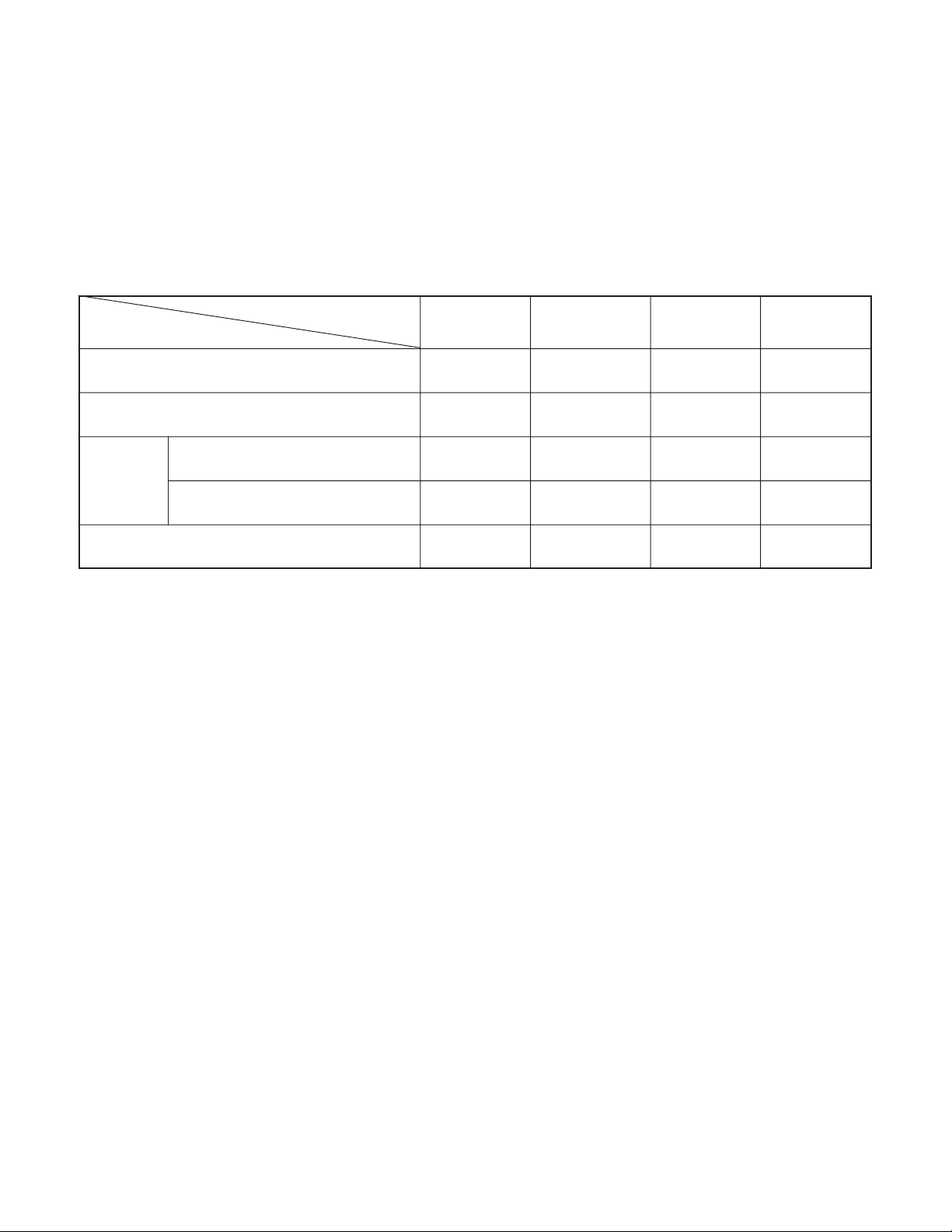
between the 8-bit microprocessor, ASIC and SPARC lite circuits.
SREQ
8-bit
Microprocessor
Fig. 5-1 Internal Bus Communication System
ASIC_SDO
ASIC_SDI
ASIC_SCK
MRST
3. Key Operaiton
For details of the key operation, refer to the instruction manual.
SCAN
SCAN
OUT
IN
0
1
2
0
UP
-
PW_TEST
123
DOWN
VREC
-
Table 5-2. Key Operation
LEFT
PLAY
TEST -
RIGHT
MENU
ASIC
4
SET
POWER
-
– 9 –
Page 10
4. Power Supply Control
The 8-bit microprocessor controls the power supply for the overall system.
The following is a description of how the power supply is turned on and off. When the battery is attached, a regulated 3.2 V
voltage is normally input to the 8-bit microprocessor (IC301) by IC302, so that clock counting and key scanning is carried out
even when the power switch is turned off, so that the camera can start up again. When the battery is removed, the 8-bit microprocessor operates in sleep mode using the backup lithum battery. At this time, the 8-bit microprocessor only carries out clock
counting, and waits in standby for the battery to be attached again. When a switch is operated, the 8-bit microprocessor supplies
power to the system as required.
The PON signal from the 8-bit microprocessor at pin (32) set to high, and then turns on the DC/DC converter. At this time, low
signal is output from pin (18) so that the ASIC is set to the reset condition. After, this pin set to high, and set to active condition.
When the power switch is turned off, the ASIC returns to the reset condition, all DC/DC converters are turned off and the power
supply to the whole system is halted.
ASIC,
memory
Power voltage
Power OFF
Power switch ON-
Auto power OFF
CAMERA
LCD monitor
Playback
Note) 4 MHz = Main clock operation, 32 kHz = Sub clock operation
3.3 V 1.8 V 1.2 V
OFF
OFF
ON
ON
Table 5-3. Camera Mode
CMOS
2.7 V (A) 1.8 V (D)
1.8 V (I/O)
OFF
OFF
ON
OFF
8 bit
CPU
3.2 V
(ALWAYS)
32KHz OFF
32KHz OFF
4 MHz ON
4 MHz ON
MONITOR
LCD
3.3 V
– 10 –
Page 11

MEMO
– 11 –
Page 12
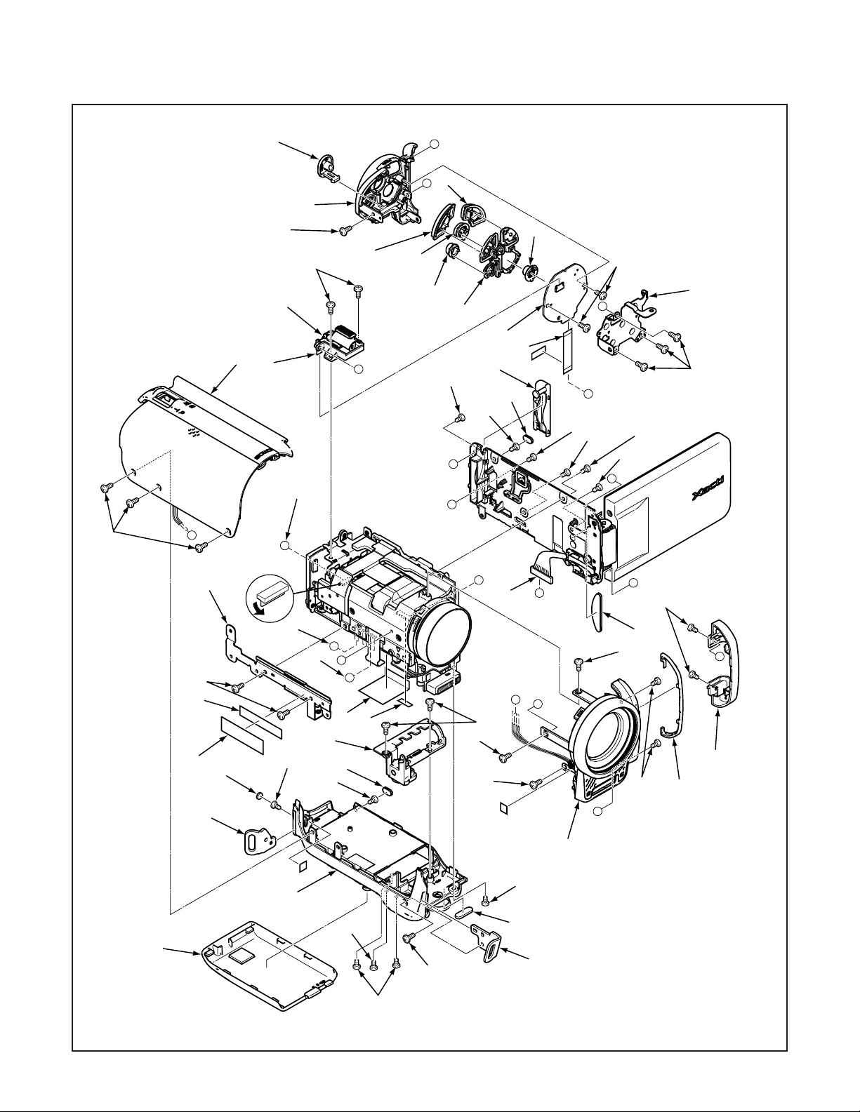
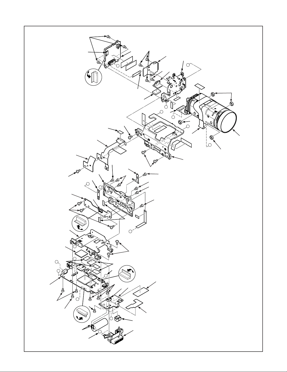
2. DISASSEMBLY
2-1. REMOVAL OF CABINET BOTTOM, CABINET TOP, CABINET BACK, TB4 BOARD AND CABINET FRONT
When assembling,
assemble order.
A → B
When assembling,
assemble order.
A → B
A
7
I
21
28
33
22
34
B
39
A
38
D
41
37
36
When assembling,
tighten the screws order.
a → b → c
31
30
F
b
A
27
B
40
23
32
35
F
26
24
3
J
c
a
29
19
24
56
D
25
J
A
20
57
E
43
42
45
15
46
13
18
14
44
B
17
6
I
47
3
H
B
G
48
16
49
H
a
G
B
54
b
53
c
55
A
9
C
5
4
54
52
51
C
When assembling,
tighten the screws order.
a → b → c
E
50
10
8
1
2
12
When assembling,
assemble order.
A → B
11
9
NOTE: Discharge a strobe capacitor with the
discharge jig (VJ8-0188) for electric shock prevention.
– 12 –
Page 13
1. Cover battery
2. Spacer bottom
3. Spacer LCD
4. Spacer LCD front
5. Two screws 1.7 x 2
6. Screw 1.7 x 7
7. Three screws 1.7 x 3
8. Screw 1.7 x 3
50. Dec joint
51. Dec line joint
52. Two screws 1.7 x 4
53. Screw 1.7 x 3
54. Two screws 1.7 x 3
55. Compl, cabinet front
56. Screw 1.7 x 3
57. Screw 1.7 x 3
9. Three screws 1.7 x 4
10. Remove the cabi bottom from the main body.
11. Screw 1.7 x 3
12. Holder strap front
13. Spacer blind
14. Screw 1.7 x 3
15. Holder strap back
16. Two screws 1.7 x 4
17. Stand
18. Remove the solder.
19. Screw 1.7 x 3
20. Screw 1.7 x 3
21. Cabinet top
22. Screw 1.7 x 3
23. Two screws 1.7 x 3
43. Spacer mic
24. Two screws 1.7 x 3
25. Flexible pwb CP1 & TB4
26. Cover SD
27. Remove the cabinet back from the main body.
28. Cover DC
29. Three screws 1.7 x 4
30. Holder back
31. Two screws 1.7 x 4
32. TB4 board
33. FPC
34. Unit, zoom
35. Flexible pwb CP1 & TB4
36. Button select
37. Holder button bas
48. Sheild tape LCD CP1
38. Button menu
39. Button rec play
40. Button movie
41. Button shutter
42. Sheild tape mic
43. Spacer mic
44. Remove the solder.
45. Two screws 1.7 x 4
46. Holder bottom
47. Spacer shield wire
48. Sheild tape LCD CP1
49. Connector
47. Spacer shield wire
42. Sheild tape mic
Cross-section drawing
Do not run.
55. Compl, cabinet front
Note:
Do not tuck the
lead wires.
– 13 –
Page 14
2-2. REMOVAL OF TB1 BOARD, TB5 BOARD, LENS, ST1 BOARD, CP1 BOARD AND TB3 BOARD
When assembling,
tighten the screws order.
a → b → c
When assembling,
tighten the screws order.
A → B
3
2
51
5
7
c
a
b
6
E
10
8
9
19
21
22
A
17
20
C
B
23
H
12
1
4
A
D
15
25
24, 26
F
B
25
16
49
A
38
52
14
46
a
B
18
B
11
45
47
14
a
47
40
13
E
42
C
b
43
39
50
48
When assembling,
tighten the screws order.
37
G
D
a → b
27
H
44
41
G
39
b
F
29
30
36
28
31
34
33
32
I
I
35
– 14 –
Page 15
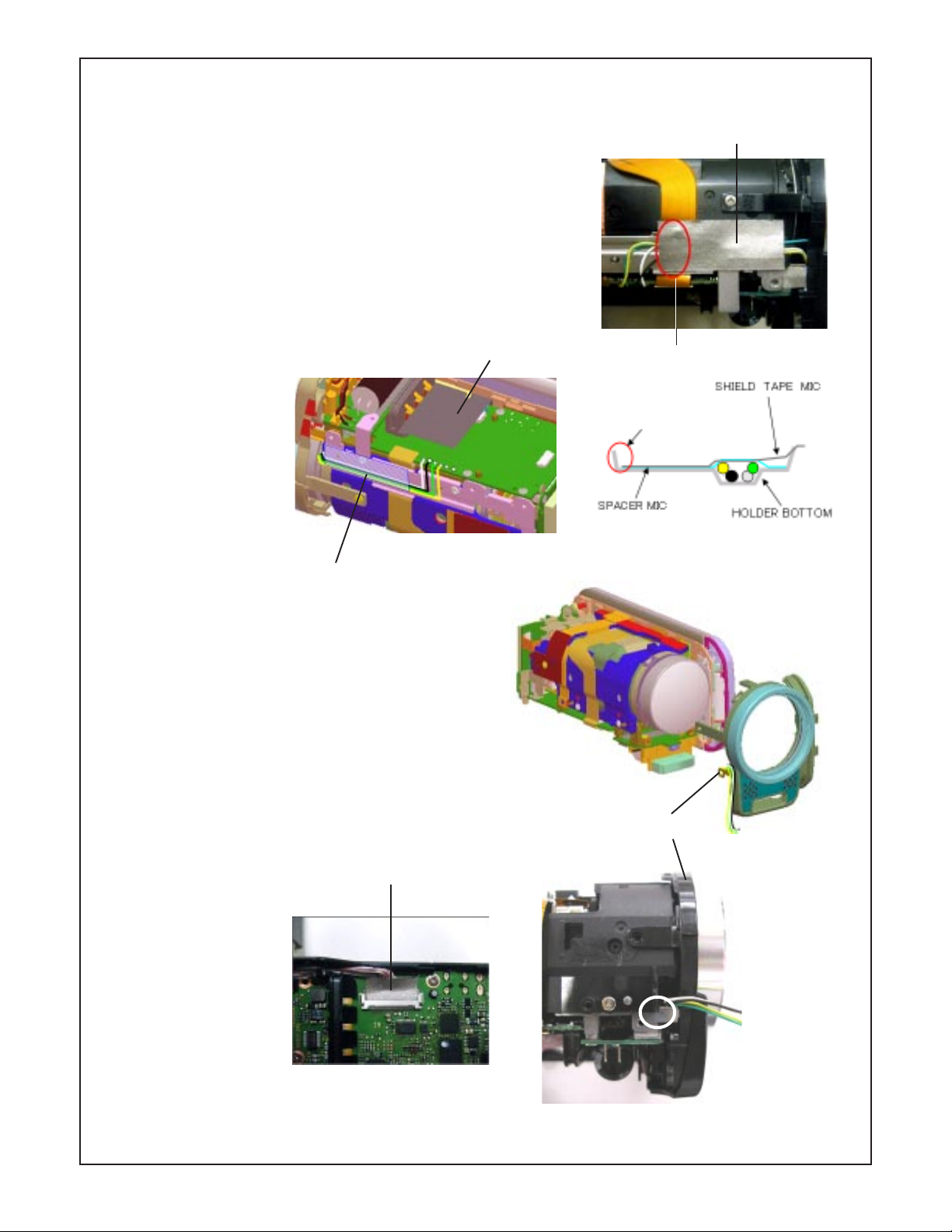
1. Shield tape VF1
2. Screw 1.7 x 3
3. Heat sink left
4. Heat sink tape top
5. Three screws 1.7 x 3
6. TB1 board
7. Flexible pwb TB1 & TB5
8. Three screws 1.7 x 2.5
9. TB5 board
10. Flexible pwb TB1 & TB5
11. Two screws 1.7 x 4
12. Screw 1.7 x 3
13. Two screws 1.7 x 3
14. Two screws 1.7 x 4
15. FPC
16. Holder lens chassis
17. Holder lens
18. Two screws 1.7 x 3
19. Holder TB1
20. Spacer CA
21. Screw 1.7 x 2.5
22. Holder CA
23. Connector
24. Remove the lens part.
25. Holder lens
26. Lens
27. Two screws 1.7 x 7
28. Screw 1.7 x 3
29. Connector
30. ST1 board
31. Spacer ST1
32. Remove the solder.
33. Assy, lamp
34. Cover triger
35. Remove the solder.
36. Spacer con ST1
37. Spacer lens right
38. Flexible pwb CP1 & TB3
39. Four screws 1.7 x 3
40. CP1 board
41. Flexible pwb CP1 & TB3
42. Heat sink rub ASIC
43. Sheild tape DDR
44. Spacer DDR
45. Screw 1.4 x 2
46. Earth jack
47. Two screws 1.7 x 3
48. Chassis bottom
49. Spacer holder TB1
50. Three screws 1.7 x 2.5
51. TB3 board
52. Chassis right
33. Assy lamp soldering order
16. Holder lens chassis
44. Spacer DDR
33. Assy lamp dressing method
38, 41. Flexible pwb CP1 & TB3
37. Spacer lens right
43. Sheild tape DDR
– 15 –
Page 16
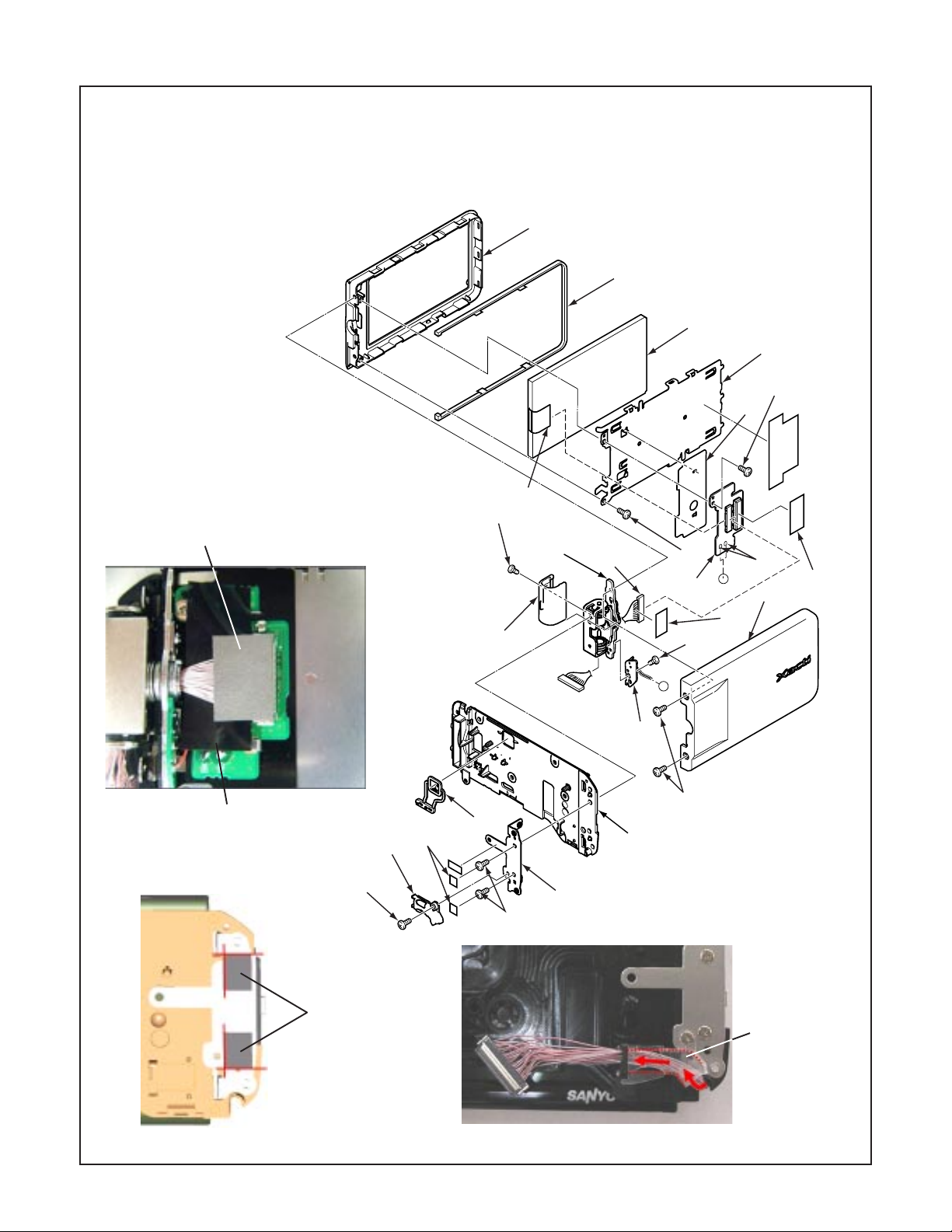
2-3. REMOVAL OF TB2 BOARD, VF1 BOARD AND LCD
1. Screw 1.7 x 2
2. Screw 1.7 x 3
3. Holder wire
4. Spacer holder joint
5. Two screws 1.7 x 3
6. Holder joint
7. Cabinet right
8. Button power
9. Cover joint
10. Two screws 1.7 x 3
11. Cover LCD back
12. Dec line A
13. Sheild tape VF1
14. Connector
13. Sheild tape VF1
15. Spacer LCD FPC
16. Remove the solder.
17. Assy, joint
When assembling,
assemble order.
A → B
18. Screw 1.7 x 2
19. TB2 board
20. FPC
26
20
1
17
B
A
9
14
12
21. Two screws 1.7 x 3
22. VF1 board
23. Spacer pwb
24. Holder LCD
25. LCD
26. Cover LCD front
When assembling,
assemble order.
A → B
25
24
21
23
B
A
21
22
16
A
11
13
18
15
15. Spacer LCD FPC
4
3
2
4. Spacer holder joint
A
19
10
8
7
6
5
3. Holder wire
– 16 –
Page 17
2-4. BOARD LOCATION
TB4 board
CP1 board
TB1 board
TB5 board
TB3 board
VF1 board
TB2 board
ST1 board
– 17 –
Page 18
3. ELECTRICAL ADJUSTMENT
Firmware
QrCode
AWB
Focus
UV Matrix
R Bright
RGB Offset
Tint
B Bright
Gain
Phase
LCD
Calibration
Upload
PAF Cal.
LCD Type
H AFC Test
VCOMDC
VCOMPP
Cal Data
Cal Mode
OK
OK
EVF
USB storage
Get
Set
VID
Set
PID
Set
Serial
Set
Rev.
Set
Setting
Language
Video Mode
VCO
Factory Code
Hall Cal.
Backrush pulse :
Set
Get
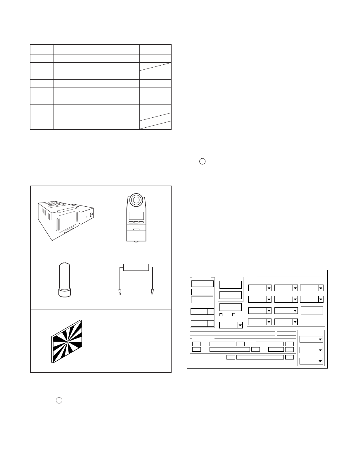
3-1. Table for Servicing Tools
Ref. No.
J-1
J-2
J-3
J-4
J-5
J-6
J-7
J-8
J-9
Name
Pattern box
Calibration software
Chroma meter
Spare lump (pattern box)
Discharge jig
Collimator
Spare lump (collimator)
Siemens star chart
ND2 filter
Number
1
1
1
1
1
1
1
1
1
Part code
VJ8-0190
VJ8-0192
VJ8-0191
VJ8-0188
VJ8-0260
VJ8-0282
3-3. Adjustment Items and Order
1. Lens Adjustment (Barcode Input)
2. Lens Adjustment (Infinity)
3. Lens Adjustment (1m)
4. Mecha Shutter Adjustment
5. WB Adjustment
6. CMOS White Point Defect Detect Adjustment
7. CMOS Black Point And White Point Defect Detect Adjust-
ment In Lighted
Note: If the lens, board and changing the part, it is necessary
to adjust again. Item 1-7 adjustments should be carried out in
sequence.
*Adjustment environment
Temperature: 25 ± 10 degrees, Humidity: 55 ± 25 %
Download the calibration software and the firmware
from the following URL.
http://www.digital-sanyo.com/overseas/service/
Place the DscCalDi.exe file, camapi32.dll file and
QrCodeInfo.dll file together into a folder of your
choice.
J-1 J-3
J-4
J-5
3-4. Setup
1. System requirements
Windows 2000 or XP or Vista
IBM R -compatible PC with pentium processor
USB port
40 MB RAM
Hard disk drive with at least 15 MB available
VGA or SVGA monitor with at least 256-color display
2. Pattern box
Turn on the switch and wait for 30 minutes for aging to take
place before using Color Pure. It is used after adjusting the
chroma meter (VJ8-0192) adjust color temperature to 3100 ±
20 K and luminosity to 900 ± 20 cd/m
the lump and its circumference are high temperature during
use and after power off for a while.
3. Computer screen during adjustment
2
. Be careful of handling
J-8
3-2. Equipment
1. AC adaptor
2. PC (IBM R -compatible PC, Windows 2000 or XP or Vista)
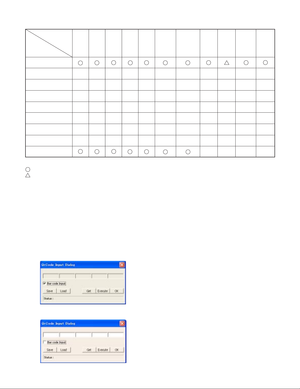
3-5. Connecting the camera to the computer
1. Use the supplied dedicated USB interface cable to connect
the camera to the computer.
2. Turn on the camera.
3. Choose the “COMPUTER”, and press the SET button.
Next, choose the “CARD READER”, and press the SET
button.
– 18 –
Page 19
3-6. The adjustment item which in necessary in part exchange
Lens
Adjust-
ment
(Barcode
Input)
Lens
Adjust-
ment
(Infinity)
Lens
Adjust-
ment
(1 m)
Mecha
Shutter
Adjust-
ment
WB
Adjust-
ment
CMOS
White Point
Defect
Detect
Adjustment
CMOS Black
Point And
White Point
Defect Detect
Adjustment
In Lighted
Factory
Cord
Setting
Language
Setting
COMPL PWB CP1
COMPL PWB VF1
COMPL PWB ST1
COMPL PWB TB1
COMPL PWB TB2
COMPL PWB TB3
COMPL PWB TB4
COMPL PWB TB5
ASSY, FLEXIBLE
PWB CA1
: Be sure to carry out the necessary adjustments after replacing the unit.
: Adjustment is possible from the menu setting screen of the camera and by using the calibration software.
USB
storage
information
registration
Reset
Setting
3-7. Updating the firmware
Check the firmware version immediately after the CP1 board has been replaced. If an old version is being used, interference and errors in operation may also occur. If an old version is being used, update it with a newer version.
Refer to
3-8. Adjust Specifications
1. Lens Adjustment (Barcode Input)
Adjustment method:
1. Double-click on the DscCalDi.exe.
2. Click the “QrCode”.
3. QrCode Input Dialog display will be displayed.
4. Deselect Bar code Input.
3-13. Firmware uploading procedure. (Page 24)
5. Enter the alphanumeric characters which are underneath
the bar code which is included with the lens.
6. Click the Execute.
7. Click the OK.
Note: The five input boxes (numbered (1) (2) (3) (4) (5) in
order starting from the left) have the following limits on input.
(1) can only contain numerical input from 0 to 2.
(2) can only contain numerical input from 0 to 2.
(3) can only contain numerical input from 1 to 2.
– 19 –
Page 20
2. Lens Adjustment (Infinity)
Camera
Collimator
Preparation:
POWER switch: ON
If using a ready-made collimator, set to infinity.
Note:
Do not vibrate during the adjustment.
If readjusting after it has already been adjusted, wait for 15
minutes or more for the unit to cool down first.
Adjustment method:
1. Set the camera so that it becomes center of the siemens
star chart in the collimator (zoom wide and tele).
(Set a distance of 0.5-1.0 cm between camera lens and
collimator lens. Do not touch the each lens.)
2. Set the camera so that it becomes center of the screen in
the collimator.
3. Double-click on the DscCalDi.exe.
4. Select “Infinity Cal.” on the LCD “Test”, and click the “Ye s ”.
5. Lens infinity adjustment value will appear on the screen.
6. Click the OK.
3. Lens Adjustment (1m) is carried out after this adjust-
ment.
Dsc Calibration
Infinity calibration :
AF_TEMP_AD_I: 480
PZ_BR: 2
AF_BR: 5
AF_I_WIDE: 69
AF_I_MID1: 257
AF_I_MID2: 126
AF_I_MID3: 213
AF_I_MID4: 203
AF_I_MID5: 187
AF_I_MID6: 121
AF_I_TELE: 195
FLAG_PZ_ADJ: 1
PZ_ADJ_INDEX: 0
IRIS_GAIN: -112
IRIS_OFFSET: -6
x
OK
Copy
Adjustment value determination is effectuated using below values.
The adjustment values fulfill the conditions below, they are determined as within specifications.
Adjustment value determination
AF_TEMP_AD_I: ATADI
ATADI: adjustment value of focus temperature A/D
(250<=ATADI<=893)
PZ_BR: PBR
PBR: adjustment value of zoom backrush pulse
(0<=PBR<=10)
AF_BR: ABR
ABR: adjustment value of focus backrush pulse
(0<=ABR<=10)
AF_I_WIDE: ZIW
ZIW: infinity adjustment value of focus at zoom position
wide (–300<=ZIW<=300)
AF_I_MID1: ZIM1
ZIM1: infinity adjustment value of focus at zoom position
middle1 (–300<=ZIM1<=300)
AF_I_MID2: ZIM2
ZIM2: infinity adjustment value of focus at zoom position
middle2 (–300<=ZIM2<=300)
AF_I_MID3: ZIM3
ZIM3: infinity adjustment value of focus at zoom position
middle3 (–300<=ZIM3<=300)
AF_I_MID4: ZIM4
ZIM4: infinity adjustment value of focus at zoom position
middle4 (–300<=ZIM4<=300)
AF_I_MID5: ZIM5
ZIM5: infinity adjustment value of focus at zoom position
middle5 (–300<=ZIM5<=300)
AF_I_MID6: ZIM6
ZIM6: infinity adjustment value of focus at zoom position
middle6 (–300<=ZIM6<=300)
AF_I_TELE: ZIT
ZIT: infinity adjustment value of focus at zoom position
tele (–250<=ZIT<=300)
FLAG_PZ_ADJ: FPZ
FPZ: flag of zoom barcode adjustment
(FPZ=1)
PZ_ADJ_INDEX: PZI
PZI: index of zoom barcode adjustment
(0<=PZI<=2)
IRIS_GAIN: g
g: adjustment value of gain (-128<=g<=127)
IRIS_OFFSET: o
o: adjustment value of offset (-128<=o<=127)
– 20 –
Page 21

3. Lens Adjustment (1m)
Camera
Preparation:
POWER switch: ON
Adjustment condition:
Siemens star chart (A3)
Fluorescent light illumination with no flicker
Illumination above the subject should be 700 lux ± 10%.
Note:
Do not vibrate during the adjustment.
If readjusting after it has already been adjusted, wait for 15
minutes or more for the unit to cool down first.
Adjustment method:
1. Set the siemens star chart 100 ± 0.5 cm from lens surface
so that it becomes center of the screen (zoom wide and
tele). Set the camera and the chart in a straight, and do not
put optical systems (mirror and conversion lens etc.)
2. Double-click on the DscCalDi.exe.
3. Click the “Focus”, and Click the “Yes ”.
4. Lens adjustment value will appear on the screen.
5. Click the OK.
100 0.5 cm
Siemens
star chart
Adjustment value determination
AF_TEMP_AD: ATAD
ATAD: adjustment value of focus temperature A/D
(250<=ATAD<=893)
AF_WIDE: ZW
ZW: adjustment value of focus at zoom position wide
(–300<=ZW<=300)
AF_MID1: ZM1
ZM1: adjustment value of focus at zoom position middle1
(–300<=ZM1<=300)
AF_MID2: ZM2
ZM2: adjustment value of focus at zoom position middle2
(–300<=ZM2<=300)
AF_MID3: ZM3
ZM3: adjustment value of focus at zoom position middle3
(–300<=ZM3<=300)
AF_MID4: ZM4
ZM4: adjustment value of focus at zoom position middle4
(–300<=ZM4<=300)
AF_MID5: ZM5
ZM5: adjustment value of focus at zoom position middle5
(–300<=ZM5<=300)
AF_MID6: ZM6
ZM6: adjustment value of focus at zoom position middle6
(–300<=ZM6<=300)
AF_TELE: ZT
ZT: adjustment value of focus at zoom position tele
(–250<=ZT<=300)
4. Mecha Shutter Adjustment
DscCalDi
Focus Result
x
!
AF_TEMP_AD: 453
AF_WIDE: 60
AF_MID1: -19
AF_MID2: -99
AF_MID3: -284
AF_MID4: -105
AF_MID5: -189
AF_MID6: -254
AF_TELE: 102
OK
Adjustment value determination is effectuated using below values.
The adjustment values fulfill the conditions below, they are determined as within specifications.
Camera
ND2 filter
Pattern box
(color viewer)
Preparation:
POWER switch: ON
Setting of pattern box:
Color temperature: 3100 ± 20 (K)
Luminance: 900 ± 20 (cd/m
2
)
Adjusting method:
1. Set a distance of 0.5-1.0 cm between the pattern box and
the camera. (Do not enter any light.)
2. Insert the ND2 filter between the camera lens and the pattern box.
– 21 –
Page 22

3. Double-click on the DscCalDi.exe.
4. Input “32” in the Cal Mode, and click Ok at the right side.
5. Click the OK.
6. Input “30” in the Cal Mode, and click Ok at the right side.
7. Click the OK.
5. WB Adjustment
Dsc Calibration
Cal Mode Results :
IRIS_LG: 12535
IRIS_LG_R1: 701
IRIS_LG_R2: 982
IR_TEMP_AD=345
IRIS_PWM1=200,166
IRIS_PWM2=143,119
IRIS_PWM3=108,98
IRIS_PWM4=89,82
IRIS_PWM5=77,72
IRIS_PWM6=68,65
OK
Copy
x
Dsc Calibration
Cal Mode Results :
MS=4580,100
MS_M=3706,3349
MS_C=2796,800
MS_C2=700,500
MS_C3=450,400
MS_C4=300,200
x
OK
Copy
Adjustment value determination is effectuated using the "MS",
“MS_M” , “ MS_C” , “MS_C2” , “ MS_C3” , “ MS_C4” ,
“IRIS_PWM1”, “IRIS_PWM2”, “IRIS_PWM3”, “IRIS_PWM4”,
“IRIS_PWM5” , “ IRIS_PWM6” , “ IR_TEMP_AD” and
“IRIS_LG_R2” values. If
MS = ms1, ms2
MS_M = ms3, ms4
MS_C = ms5, ms6
MS_C2 = ms7, ms8
MS_C3 = ms9, ms10
MS_C4 = ms11, ms12
IRIS_PWM1 = s1, s2
IRIS_PWM2 = s3, s4
IRIS_PWM3 = s5, s6
IRIS_PWM4 = s7, s8
IRIS_PWM5 = s9, s10
IRIS_PWM6 = s11, s12
IR_TEMP_AD = itad
IRIS_LG_R2 = iris_lg2
the adjustment values fulfill the conditions below, they are
determined as within specifications.
Adjustment value determination
2000<=ms1<=6500, 100<=ms2<=4100,
1800<=ms3<=5800, 1500<=ms4<=5500,
1000<=ms5<=5000, 800<=ms6<=4800,
700<=ms7<=4700, 500<=ms8<=4500,
450<=ms9<=4450, 400<=ms10<=4400,
300<=ms11<=4300, 200<=ms12<=4200
0<=s1<=255, 0<=s2<=255, 0<=s3<=255, 0<=s4<=255,
0<=s5<=255, 0<=s6<=255, 0<=s7<=255, 0<=s8<=255,
0<=s9<=255, 0<=s10<=255, 0<=s11<=255, 0<=s12<=255
ms2<ms12<ms11<ms10<ms9<ms8<ms7<ms6<ms5<ms4<ms3<ms1
s1>s2>s3>s4>s5>s6>s7>s8>s9>s10>s11>s12
250<=itad<=893
900<=iris_lg2<=1100
Adjustment values other than the above are irrelevant.
Camera
Pattern box
(color viewer)
Preparation:
POWER switch: ON
Setting of pattern box:
Color temperature: 3100 ± 20 (K)
Luminance: 900 ± 20 (cd/m
2
)
Adjusting method:
1. Set a distance of 0.5-1.0 cm between the pattern box and
the camera. (Do not enter any light.)
2. Double-click on the DscCalDi.exe.
3. Input “22” in the Cal Mode, and click Ok at the right side.
4. Click the OK.
5. Input “25” in the Cal Mode, and click Ok at the right side.
6. Click the OK.
Dsc Calibration
OK
Copy
Cal Mode Results:
WB=342,522,623
CHECK=129,127,127
Dsc Calibration
x
Cal Mode Results:
WB_ND=0,0,0
FLAG_FS_ADJ=17
CHECK_ND=129,129,0
Adjustment value determination is effectuated using the
“CHECK" and “CHECK_ND” values. If
CHECK= wc0, wc1, wc2
CHECK_ND= wnc0, wnc1, wnc2
the adjustment values fulfill the conditions below, they are determined as within specifications.
– 22 –
x
OK
Copy
Page 23

Adjustment value determination
wc0=128 ± 2, wc1=128 ± 2, wc2<=255
wnc0=128 ± 2, wnc1=128 ± 2, wnc2<=255
Adjustment values other than the above are irrelevant.
6. CMOS White Point Defect Detect Adjustment
Preparation:
POWER switch: ON
Adjustment method:
1. Double-click on the DscCalDi.exe.
2. Select “CCD Defect” on the LCD “Test”, and click the “Ye s ”.
3. After the adjustment is completed, OK will display.
4. Click the OK.
7. CMOS Black Point And White Point Defect Detect
Adjustment In Lighted
3-9. Factory Code Setting
1. Check the "Factory Code" display within the Setting group.
2. For U.S.A., Canada and NTSC general area
If "FC_SANYO_U" does not appear, click on the " " mark
located on the right of the "Factory Code" display BOX and
select "FC_SANYO_U".
3. For Europe and PAL general area
If "FC_SANYO_EX" does not appear, click on the " " mark
located on the right of the "Factory Code" display BOX and
select "FC_SANYO_EX".
3-10. Language Setting
1. Click on the " " mark located on the right of the
"Language" display BOX.
2. Select language. (Default is English.)
3. End "DscCal" and remove the camera before turning the
camera power OFF.
Camera
Pattern box
(color viewer)
Preparation:
POWER switch: ON
Setting of pattern box:
Color temperature: 3100 ± 20 (K)
Luminance: 900 ± 20 (cd/m
2
)
Adjusting method:
1. Set a distance of 0.5-1.0 cm between the pattern box and
the camera.
2. Double-click on the DscCalDi.exe.
3. Select “CCD Black” on the LCD “Test”, and click the “Ye s ”.
4. After the adjustment is completed, the number of defect
will appear.
5. Click the OK.
Calibration
AWB
Focus
UV Matrix
Cal Mode
Cal Data
USB storage
VID
Get
PID
Set
Backrush pulse :
OK
OK
Upload
Firmware
QrCode
PAF Cal.
EVF
LCD Type
Get
LCD
R Bright
RGB Offset
Tint
VCO
H AFC Test
Serial
Set
Set
Rev.
B Bright
Gain
Phase
Set
Set
Set
VCOMDC
VCOMPP
Hall Cal.
Setting
Language
Video Mode
Factory Code
3-11. Reset Setting
Carry out reset settings after replacing CP1 board.
1. Turn on the camera.
2. Set the NORMAL mode, and press the MENU button.
3. Choose the OPTION MENU 3.
4. Choose the RESET SETTINGS, and press the SET button.
5. Select RESET, and press the SET button.
3-12. The Compulsive boot starting method
1. Keep MENU button, SET button, and SHUTTER button depressed while switching on the power.
2. Connect the camera and the computer with USB cable.
– 23 –
Page 24

3-13. Firmware uploading procedure
1. Uploading the firmware should be carried out if the version
number (COMPL PWB XX-X) on the replacement circuit
board is lower than the version of the distributed firmware.
For XX-X, enter the name of the circuit board containing the
firmware.
2. The firmware is distributed by e-mail in self-extracting archive
format. Change the extension of the distributed file to .EXE
and save it in your preferred folder.
3. When you double-click the saved file, the firmware (binary
file) will be saved in the same folder.
4. The firmware must not be distributed without permission.
1. Overwriting firmware from the SD card
Preparation:
SD card: SD card with firmware rewritten into the root directory
Data: S317Nxxx.BIN (xxx: version)
Overwriting method:
1. Insert the above SD card.
2. Turn on the camera.
3. Set the NORMAL mode.
4. Press the MENU button.
5. Choose the OPTION MENU 3.
6. Choose the FORMAT.
7. Toggle the SET button to the left for 2 seconds. FIRMWARE
UPDATE will display.
8. Choose YES.
9. Press the SET button. Update is starting.
Note:
Do not turn off the camera’s power or remove the SD card
while the firmware is being updated.
The power will turn off after the update is complete.
2. Overwriting firmware from the calibration software
Preparation:
PC with overwriting firmware copied to the preferred folder in
the HD.
Data: S317Nxxx.BIN (xxx: version)
Overwriting method:
1. Connect the camera’s USB/AV terminal to the computer’
USB connector.
2. The USB Connection screen appears on the camera’s LCD
monitor. Choose the “COMPUTER”, and press the SET
button. Next, choose the “CARD READER”, and press the
SET button.
3. Double-click on the DscCalDi.exe.
4. Click the Firmware.
5. Choose the fimware file to use for overwriting, and click
the Yes.
6. Update is starting. The message will appear, and choose
OK.
7. After the update is complete, disconnect the USB cable
and turn the camera’s power off.
Note:
Do not turn off the camera’s power while the firmware is being updated.
– 24 –
Page 25

4. USB STORAGE INFORMATION REGISTRATION
USB storage data is important for when the camera is connected to a computer via a USB connection.
If there are any errors in the USB storage data, or if it has not
been saved, the USB specification conditions will not be satisfied, so always check and save the USB storage data.
Preparation:
POWER switch: ON
Adjustment method:
1. Connect the camera to a computer. (Refer to 3-5. Connecting the camera to the computer on the page 18.)
2. Double-click on the DscCalDi.exe.
3. Click on the Get button in the USB storage window and
check the USB storage data.
VID: SANYO
PID: FH1
Serial:
Rev. : 1.00
4. Check the “Serial” in the above USB storage data. If the
displayed value is different from the serial number printed
on the base of the camera, enter the number on the base
of the camera. Then click the Set button.
5. Next, check VID, PID and Rev. entries in the USB storage
data. If any of them are different from the values in 3. above,
make the changes and then click the corresponding Set
button.
Calibration
AWB
Focus
UV Matrix
Cal Mode
Cal Data
USB storage
VID
Get
PID
Set
Backrush pulse :
OK
OK
Upload
Firmware
QrCode
PAF Cal.
EVF
LCD Type
Get
LCD
R Bright
RGB Offset
Tint
VCO
H AFC Test
Serial
Set
Set
Rev.
B Bright
Gain
Phase
Set
Set
Set
VCOMDC
VCOMPP
Hall Cal.
Setting
Language
Video Mode
Factory Code
– 25 –
Page 26

5. TROUBLESHOOTING GUIDE
POWER LOSS INOPERTIVE
PUSH THE POWER
SW FOR A WHILE
IC301-43
(SCAN OUT1)
PULSE INPUT
NO
IC302-7 5.3 V
(BOOST 5.3 V)
YES
IC301-9, 35, 59
(VDD)
HIGH
IC301-53
(RESET)
HIGH
IC301-49
(BAT OFF)
HIGH
IC301-55
OSCILLATION
YES
YES
NO
LOW
LOW
LOW
NO
CHECK S3003
CHECK IC501
CHECK IC302
CHECK IC302, RB312
CHECK RB312
CHECK X3002
TAKING INOPERATIVE
PUSH SHUTTER
BUTTON
IC301-51, 23
(KEY_1st, KEY_2nd)
LEVEL INPUT
YES
IC501-F6 (PON)
IC503-4 (PAON2)
IC504-1 (PAON1)
HIGH
SERIAL
COMMUNICATION
OK
CHECK CP1 DMA
BLOCK
NO
LOW
CHECK IC301, IC101,
NG
CHECK SW UNIT
PWA BLOCK
CHECK IC301,
CP1 DMA BLOCK
CHECK IC301
NO PICTURE
X1102
CHECK
OSCILLATION
OK
IC301-64, 63
(ASIC_SO, ASIC_SI)
OK
CHECK SOLDERING
OF MEMORY
EACH PIN
NG
MAIN CLOCK FOR SYSTEM OPERATION
NO OPERATION IF ABSENT
INCORRECT HANDSHAKING
NG
BETWEEN 8-BIT CPU AND ASIC
CHECK EACH INTERFACE
– 26 –
Page 27

MEMO
– 27 –
Page 28

6. PARTS LIST (R)
LOCATION PARTS NO. DESCRIPTION
ACCESSORIES & PACKING MATERIALS
1 636 124 1403 STRAP BELT-SG314/U
2 636 125 0108 DISC,CD-ROM XSD G317 U(N.S.P.) ,
3 645 098 9612 BATTERY,RECHARGE,LI-ION
4 645 093 6180 CABLE,DSC A/V-SG211
5 645 099 3350 CABLE,DSC USB
OR 645 099 3367 CABLE,DSC USB
6 645 098 9117 CABLE,DSC COMPONENT-SG313
7 645 076 0235 CORD,POWER-1.5MK,
OR 645 098 8721 CORD,POWER-1.2MK,
7 645 084 0104 CORD,POWER-1.8MK,VPC-FH1BK,VPC-FH1
OR 645 098 8714 CORD,POWER-1.9MK,VPC-FH1BK,VPC-FH1
8 645 099 5835 ADAPTOR,AC-DC(BOX)
9 645 093 6746 REMOCON,INFRARED,WIHT COVER BATTERY
10 636 103 1783 STRAP CAP LENS-SG112/J
11 636 123 0414 ASSYL,CAP LENS-SG314
12 645 099 4029 CABLE,DSC USB HOST-SG313
13 645 094 6691 CORE,CLAMP,FOR HDMI(TV END)
14 645 095 3620 CORE,FERRITE,FOR HDMI(CAMERA END)
9051 636 124 5302 INSTRUCTION MANUAL,
9052 636 124 5319 INSTRUCTION MANUAL,
9053 636 124 5289 INSTRUCTION MANUAL,CAMERA SOFT GB,
9056 636 121 1925 INSTRUCTION MANUAL,Xacti library(English)
636 124 5890 CARTON INNER-SG317/EX,
636 124 5883 CARTON INNER-SG317/U,
636 077 8139 CUSHION SHEET-SX774/KRO
636 122 9326 REINFORCE PAD,A-SG314/J
636 119 2361 LABEL GOLD TEXT-SG218/GX2,
636 126 7595 LABEL GOLD MODEL-SG317/U2,
Xacti software,PDF instruction manual and
quick guide(English,French,German,Spanish,
Italian,Dutch,Portuguese,Russian,Turkish,Korean,
Traditional chinese,Simplified chinese
Note:Turkish is only a quick guide.)
VPC-FH1EXBK,VPC-FH1EX
VPC-FH1EXBK,VPC-FH1EX
SIMPLE MANUAL SHEET 8,QUICK GUIDE 8,
Dutch,English,French,German,Italian,
Russian,Spanish,Portuguese)
SIMPLE MANUAL SHEET 4, QUICK GUIDE 4,
Chinese (Simplified),Chinese (Traditional),
Korean,Turkish
CAMERA (English)
EXCEPT VPC-FH1BK,VPC-FH1
VPC-FH1BK,VPC-FH1
VPC-FH1,VPC-FH1EX,VPC-FH1GX
VPC-FH1,VPC-FH1EX,VPC-FH1GX
28
Page 29

1
2
3
4
7
8
5
9
6
10
11
12
13
14
29
Page 30

LOCATION PARTS NO. DESCRIPTION LOCATION PARTS NO. DESCRIPTION
CABINET & CHASSIS PARTS 1
1 636 125 8289 LABEL CAUTION-SG217/U
2 636 125 6056 ASSY,CABI BOTTOM-SG317,
VPC-FH1BK,VPC-FH1EXBK,VPC-FH1GXBK
2 636 125 6063 ASSY,CABI BOTTOM-SG317/J2,
VPC-FH1,VPC-FH1EX,VPC-FH1GX
3 636 124 8297 ASSY,COVER BATTERY-SG317,
VPC-FH1BK,VPC-FH1EXBK,VPC-FH1GXBK
3 636 124 8341 ASSY,COVER BATTERY-317J2,
VPC-FH1,VPC-FH1EX,VPC-FH1GX
4 636 121 5442 STAND-SG314/J,
VPC-FH1BK,VPC-FH1EXBK,VPC-FH1GXBK
4 636 124 8433 STAND-SG317/J2,
VPC-FH1,VPC-FH1EX,VPC-FH1GX
5 636 121 5350 HOLDER STRAP FRONT-SG314
6 636 126 0633 SPACER BOTTOM-SG314/JO
7 636 127 5293 SPACER STRAP-SG317
8 636 121 5367 HOLDER STRAP BACK-SG314/J
9 636 125 8685 SPACER BLIND-SG314/J,
VPC-FH1BK,VPC-FH1EXBK,VPC-FH1GXBK
9 636 125 8692 SPACER BLIND-SG317/J2,
VPC-FH1,VPC-FH1EX,VPC-FH1GX
10 636 126 2439 SPACER LCD-SG314/J
11 636 127 4890 SHIELD TAPE MIC-SG317
12 636 122 9340 SPACER MIC-SG314/J
13 636 121 5428 HOLDER BOTTOM-SG314/J
14 636 126 0671 SPACER SHILD WIRE-SG314/J
15 636 127 4883 SHIELD TAPE LENS-SG317
16 636 124 7566 COMPL,CABINET FRONT-SG317,
VPC-FH1BK,VPC-FH1EXBK,VPC-FH1GXBK
16 636 124 7665 COMPL,CABINET FRONT-SG317,
VPC-FH1,VPC-FH1EX,VPC-FH1GX
17 636 121 8184 DEC LINE JOINT-SG317/J
18 636 121 8412 DEC JOINT-SG317/J,
VPC-FH1BK,VPC-FH1EXBK,VPC-FH1GXBK
18 636 126 4006 DEC JOINT-SG317/J2,
VPC-FH1,VPC-FH1EX,VPC-FH1GX
19 636 124 7634 COMPL,CABINET TOP-SG317,
VPC-FH1BK,VPC-FH1EXBK,VPC-FH1GXBK
19 636 124 8150 COMPL,CABINET TOP-SG317,
VPC-FH1,VPC-FH1EX,VPC-FH1GX
20 645 099 0168 UNIT,ZOOM-SG314/J
21 636 126 2446 SPACER LCD FRONT-SG314/J
22 636 121 4940 COVER SD-SG314/J
23 636 121 5381 HOLDER BACK-SG314/J
24 636 122 6356 FLEXIBLE PWB CP1&TB4SG314
25 636 127 5255 SHIELD TAPE SW1-SG317
26 636 122 6974 COMPL PWB,TB-4
27 636 121 4766 BUTTON SELECT-SG314/J,
VPC-FH1BK,VPC-FH1EXBK,VPC-FH1GXBK
27 636 124 7986 BUTTON SELECT-SG317/J2,
VPC-FH1,VPC-FH1EX,VPC-FH1GX
28 636 121 5916 HOLDER BUTTON BAS-SG314/J
29 636 121 4735 BUTTON MENU-SG314/J,
VPC-FH1BK,VPC-FH1EXBK,VPC-FH1GXBK
29 636 124 7955 BUTTON MENU-SG317/J2,
VPC-FH1,VPC-FH1EX,VPC-FH1GX
30 636 121 4773 BUTTON REC PLAY-SG314/J,
VPC-FH1BK,VPC-FH1EXBK,VPC-FH1GXBK
30 636 124 7993 BUTTON REC PLAY-SG317/J2,
VPC-FH1,VPC-FH1EX,VPC-FH1GX
31 636 121 4742 BUTTON SHUTTER-SG314/J,
VPC-FH1BK,VPC-FH1EXBK,VPC-FH1GXBK
31 636 124 7962 BUTTON SHUTTER-SG317/J2,
VPC-FH1,VPC-FH1EX,VPC-FH1GX
32 636 121 4759 BUTTON MOVIE-SG314/J,
VPC-FH1BK,VPC-FH1EXBK,VPC-FH1GXBK
32 636 124 7979 BUTTON MOVIE-SG317/J2,
VPC-FH1,VPC-FH1EX,VPC-FH1GX
33 636 124 7931 CABINET BACK-SG317/J,
VPC-FH1BK,VPC-FH1EXBK,VPC-FH1GXBK
33 636 124 7948 CABINET BACK-SG317/J2,
VPC-FH1,VPC-FH1EX,VPC-FH1GX
34 636 121 4964 COVER DC-SG314/J,
VPC-FH1BK,VPC-FH1EXBK,VPC-FH1GXBK
34 636 124 8006 COVER DC-SG317/J2,
VPC-FH1,VPC-FH1EX,VPC-FH1GX
101 411 178 9403 SCR S-TPG PAN PCS 1.7X4.0,
VPC-FH1,VPC-FH1EX,VPC-FH1GX
101 411 193 2106 SCR S-TPG PAN PCS 1.7X4.0,
VPC-FH1BK,VPC-FH1EXBK,VPC-FH1GXBK
102 411 175 5705 SCR PAN PCS 1.7X3,
VPC-FH1,VPC-FH1EX,VPC-FH1GX
102 411 194 8206 SCR PAN PCS 1.7X3,
VPC-FH1BK,VPC-FH1EXBK,VPC-FH1GXBK
103 412 078 7902 SPECIAL SCREW-1.7X3.0
104 411 218 4405 SCR S-TPG PAN PCS 1.7X7
105 411 178 6204 SCR PAN PCS 1.7X4
106 411 175 5705 SCR PAN PCS 1.7X3
107 411 177 9503 SCR S-TPG PAN PCS 1.7X3
108 411 194 8206 SCR PAN PCS 1.7X3
109 411 178 9403 SCR S-TPG PAN PCS 1.7X4.0
113 411 184 0005 SCR PAN PCS 1.7X2.0,
VPC-FH1,VPC-FH1EX,VPC-FH1GX
113 411 194 8404 SCR PAN PCS 1.7X2.0,
VPC-FH1BK,VPC-FH1EXBK,VPC-FH1GXBK
30
Page 31

34
33
D
102
102
19
20
106
106
32
A
30
29
28
31
27
109
F
26
10
24
109
108
23
106
109
E
C
108
22
25
F
106
D
A
113
21
SG317/J PARTS LIST 1
13
105
113
B
105
107
E
14
B
11
9
103
105
12
104
102
102
10
4
107
106
15
18
17
105
C
16
8
7
3
102
102
2
101
101
1
101
6
5
Cabinet 1
31
Page 32

LOCATION PARTS NO. DESCRIPTION LOCATION PARTS NO. DESCRIPTION
CABINET & CHASSIS PARTS 2
25 636 127 5255 SHIELD TAPE SW1-SG317
35 636 121 5268 HOLDER WIRE-SG314/J
36 636 127 3152 SPACER HOLDER JOINT-SG314
37 636 127 4630 SHIELD TAPE HINJI-SG317
38 636 121 5411 HOLDER JOINT-SG314/J
39 636 121 4780 BUTTON POWER-SG314/J
40 636 121 8085 CABINET RIGHT-SG317/J
41 636 121 5336 ASSY,JOINT-SG314/J
42 636 106 6310 ASSY,SHIELD WIRE CP1-VF1
43 636 127 4586 SHIELD TAPE VF1-SG317
44 636 127 2667 ASSY,COVER LCD B SV-SG317,
VPC-FH1BK,VPC-FH1EXBK,VPC-FH1GXBK
44 636 127 2681 ASSY,COVER LCD B SV-SG317,
VPC-FH1,VPC-FH1EX,VPC-FH1GX
45 636 122 6950 COMPL PWB,TB-2
46 636 124 8181 COVER JOINT-SG317/J,
VPC-FH1BK,VPC-FH1EXBK,VPC-FH1GXBK
46 636 124 8198 COVER JOINT-SG317/J2,
VPC-FH1,VPC-FH1EX,VPC-FH1GX
47 645 099 2308 ASSY,LAMP-SG314
48 404 120 5400 ELECT 60U A 300V
49 636 068 0265 COVER TRIGER-SX612/J
50 636 126 0688 SPACER ST1-SG314/J
51 636 121 5251 SPACER CON ST1-SG314/J
52 636 122 6936 COMPL PWB,ST-1
53 636 127 4906 SHIELD TAPE LCD CP1-SG317
54 636 125 0856 COMPL PWB,CP-1 F/W
55 636 127 2421 SPACER DDR-SG317/J
56 636 127 2438 SHIELD TAPE DDR-SG317/J
57 636 121 5329 HEAT SINK RUB ASIC-SG314
58 636 121 5183 CHASSIS BOTTOM-SG314/J
59 636 122 6967 COMPL PWB,TB-3
60 636 121 5176 CHASSIS RIGHT-SG314/J
61 636 127 8478 SPACER LENS RIGHT-SG317/J
62 636 124 8488 EARTH JACK-SG317/J
63 636 124 7474 SPACER HOLDER TB1-SG317/J
64 636 127 4616 SPACER LCD FPC-SG317
65 636 122 6929 COMPL PWB,VF-1
66 636 121 5237 SPACER PWB-SG314/J
67 636 127 4609 SHIELD TAPE LCD-SG317
68 636 121 5404 HOLDER LCD-SG314/J
69 645 098 7229 LCD(990000412)
70 636 121 8177 DEC LINE A-SG317/J
71 636 127 2636 ASSY,COVER LCD F SV-SG317
72 636 121 8238 HOLDER LENS CHASSIS-SG317
73 636 127 4913 SPACER HOLDER LENS-SG317
74 636 124 7535 HEAT SINK LEFT-SG317/J
75 636 124 7559 HEAT SINK TAPE TOP-SG317
76 636 127 4586 SHIELD TAPE VF1-SG317
77 636 124 8679 ASSY,FPC CA1 SV-SG317
78 636 105 2207 HOLDER LENS-SG211/J
79 636 127 5156 SPACER LENS FPC-SG317/J
80 636 121 5374 HOLDER TB1-SG314/J
81 636 121 8245 HOLDER CA-SG317/J
82 636 121 5282 SPACER CA-SG314/J
83 636 122 6981 COMPL PWB,TB-5
84 636 124 7283 FLEXIBLE PWB TB1&TB5SG317
85 636 127 5279 SHIELD TAPE TB1-SG317
86 636 127 5286 SPACER TB1-SG317
87 636 122 6943 COMPL PWB,TB-1
88 636 127 4647 SHIELD TAPE PW-SG317
89 636 122 6349 FLEXIBLE PWB CP1&TB3SG314
102 411 175 5705 SCR PAN PCS 1.7X3,
VPC-FH1,VPC-FH1EX,VPC-FH1GX
102 411 194 8206 SCR PAN PCS 1.7X3,
VPC-FH1BK,VPC-FH1EXBK,VPC-FH1GXBK
104 411 218 4405 SCR S-TPG PAN PCS 1.7X7
105 411 178 6204 SCR PAN PCS 1.7X4
106 411 175 5705 SCR PAN PCS 1.7X3
107 411 177 9503 SCR S-TPG PAN PCS 1.7X3
109 411 178 9403 SCR S-TPG PAN PCS 1.7X4.0
110 411 199 0601 SCR TIN 1.7X2,
VPC-FH1BK,VPC-FH1EXBK,VPC-FH1GXBK
110 411 199 0700 SCR TIN 1.7X2,
VPC-FH1,VPC-FH1EX,VPC-FH1GX
111 411 184 0005 SCR PAN PCS 1.7X2.0
112 411 181 2705 SCR PAN PCS-1.4X2
114 411 176 1003 SCR PAN PCS 1.7X2.5
32
Page 33

106
87
106
84
114
106
114
86
81
85
82
73
114
114
B
C
83
78
80
25
A
79
78
78
107
57
56
114
55
74
59
58
75
D
76
63
106
73
D
73
77
78
72
105
73
71
70
69
107
68
67
109
60
A
B
61
106
106
62
109
112
106
107
89
61
114
104
88
104
110
46
41
66
42
64
65
44
43
C
54
106
106
SG317/J PARTS LIST 1
53
106
48
111
55
56
106
52
49
47
50
51
106
39
35
40
36
37
33
106
36
106
38
45
111
102
102
Cabinet 2
Page 34

ELECTRICAL PARTS
Note:
1. Materials of Capacitors and Resistors are abbreviated as follows ;
Resistors Capacitors
MT-FILM Metallized Film Resistor MT-POLYEST Metallized Polyester Capacitor
MT-GLAZE Metallized Glaze Resistor MT-COMPO Metallized Composite Capacitor
OXIDE-MT Oxide Metallized Film Resistor TA-SOLID Tantalum Solid Capacitor
2. Tolerance of Capacitor (10pF over) and Resistor are noted with follow symboles.
F ............1% G ............2% J ............5% K ............10%
M ..........20% N ..........30% Z ..........+80% ~ -20%
3. Capacitors
U : µF P : pF
4. Inductors
UH : µH MH : mH
5. N.S.P. : Not available as service parts.
LOCATION PARTS NO. DESCRIPTION LOCATION PARTS NO. DESCRIPTION
COMPL PWB,CP-1 F/W
636 125 0856
(VARISTORS)
VA101 308 050 0507 VARISTOR AVR-M1005C080MT
VA102 308 050 0507 VARISTOR AVR-M1005C080MT
VA131 308 050 1207 VARISTOR AVR-M1608C120MT
(SEMICONDUCTORS)
Q1001 305 181 4909 TR 2SK3541
Q1301 305 168 3703 TR DTC144EM
OR 305 216 1200 TR RN1104MFV
OR 305 172 4703 TR UNR32A3
Q1501 305 164 2809 TR EMX1
Q1502 305 172 8800 TR 2SC5658-R
OR 305 172 8909 TR 2SC5658-S
OR 305 186 7707 TR 2SC5609 00
Q1503 305 164 2809 TR EMX1
Q1504 305 172 8800 TR 2SC5658-R
OR 305 172 8909 TR 2SC5658-S
OR 305 186 7707 TR 2SC5609 00
Q1505 305 172 8800 TR 2SC5658-R
OR 305 172 8909 TR 2SC5658-S
OR 305 186 7707 TR 2SC5609 00
Q1506 305 172 8800 TR 2SC5658-R
OR 305 172 8909 TR 2SC5658-S
OR 305 186 7707 TR 2SC5609 00
Q1507 305 157 1406 TR 2SA2018
Q1508 305 157 1406 TR 2SA2018
Q1509 305 157 1406 TR 2SA2018
Q1902 405 218 3902 TR UP0431300
OR 305 167 0406 TR EMD12
OR 305 216 2108 TR RN4984FE
Q3001 305 210 5709 TR UP0KG8D
OR 305 217 3906 TR HN2E07JE
OR 305 200 9007 TR EML17
Q3003 405 218 3902 TR UP0431300
OR 305 167 0406 TR EMD12
OR 305 216 2108 TR RN4984FE
Q3005 305 186 7301 TR UP04213 00
OR 305 181 1205 TR NSBC144EDXV6T5
OR 305 173 4009 TR PEMH2
OR 305 166 9509 TR EMH2
Q5003 405 218 4701 TR SSM3J120TU
Q5004 305 181 4909 TR 2SK3541
Q5007 405 219 2706 TR MCH5835-E
Q5008 305 200 6006 TR UP03397
Q5009 305 184 6009 TR UP03396
Q5010 405 218 2707 TR UPA650TT-A
Q5011 405 218 2707 TR UPA650TT-A
Q5012 305 208 9702 TR SSM3J16TE
Q5013 305 181 4909 TR 2SK3541
AL-SOLID Aluminum Solid Capacitor
NP-ELECT Non-Polarized Electrolytic Capacitor
OS-SOLID Aluminum Solid Capacitors with Organic
Semiconductive Electrolytic Capacitor
DL-ELECT Double Layered Electrolytic Capacitor
POS-SOLID Polymerized Organic Semiconductor Capacitor
Q5014 305 169 4501 TR DTC114EM
OR 305 216 1101 TR RN1102MFV
OR 305 172 4604 TR UNR32A1
Q5015 305 168 3703 TR DTC144EM
OR 305 216 1200 TR RN1104MFV
OR 305 172 4703 TR UNR32A3
Q5016 305 181 4909 TR 2SK3541
Q5017 305 168 3703 TR DTC144EM
OR 305 216 1200 TR RN1104MFV
OR 305 172 4703 TR UNR32A3
Q5019 405 218 2707 TR UPA650TT-A
Q5020 305 181 4909 TR 2SK3541
Q5021 405 220 8308 TR MCH6428-E
Q5201 405 218 2707 TR UPA650TT-A
Q5202 305 206 7700 TR SI3473DV-E3
Q5203 405 218 2707 TR UPA650TT-A
Q5204 305 181 4909 TR 2SK3541
(INTEGRATED CIRCUITS)
IC101 409 696 4802 IC EV3HB,BGA (N.S.P)
IC102 410 671 3802 IC K4X51323PG-8GC8,BGA (N.S.P)
IC103 410 671 3802 IC K4X51323PG-8GC8,BGA (N.S.P)
IC104 309 635 9205 IC TC7MH273FK(EL,K)
IC111 409 694 3005 IC AK8128
IC121 409 695 1604 IC S29PL064J60BFI120#,BGA (N.S.P)
IC131 410 640 8005 IC S1R72V17B00A200,BGA (N.S.P)
IC132 309 488 5805 IC TC7WH32FK
IC181 309 650 3509 IC TK70630HC-G
IC182 409 697 3101 IC AK4649ECB-L,BGA (N.S.P)
IC191 410 671 2508 IC TDA9989BET/C1,518,BGA (N.S.P)
IC301 410 620 7202 IC LC87F2832AUFL64TBM-E,BGA (N.S.P)
IC302 309 611 7607 IC NJU7286ARB1
IC305 409 695 0102 IC MAX17022ETA+
IC501 410 667 4905 IC UPD168805FC-AN2-A,BGA (N.S.P)
IC502 409 686 6205 IC SC4624MLT,LLC (N.S.P)
IC503 409 695 6401 IC XC9235C18CE
IC504 409 695 6906 IC NJM2877F3-27
IC521 409 695 5800 IC MAX8601ETD+
IC951 410 676 4507 IC LC898200A-TBM-H,BGA (N.S.P)
IC952 409 685 5308 IC XC6221S04XG
(DIODES)
D1501 307 205 2809 DIODE RB520S-30
OR 307 221 0100 DIODE MA2SD24
D1901 407 261 8903 DIODE RB520S-30FJ
D5001 307 223 5509 DIODE MA2Z720
D5002 307 250 1802 DIODE RB496EA
D5003 307 248 0701 DIODE MA21D3800
D5007 307 250 0706 DIODE DRB060M-30
D5013 407 261 8903 DIODE RB520S-30FJ
D5014 407 261 8903 DIODE RB520S-30FJ
D5201 307 248 2408 ZENER DIODE EDZ7.5B
D5202 307 248 2408 ZENER DIODE EDZ7.5B
D5203 307 248 2408 ZENER DIODE EDZ7.5B
34
Page 35

LOCATION PARTS NO. DESCRIPTION LOCATION PARTS NO. DESCRIPTION
D5204 307 248 0701 DIODE MA21D3800
D5301 307 248 0701 DIODE MA21D3800
(OSCILLATORS)
X1102 645 094 0170 OSC,CRYSTAL 48.00000MHZ
X1901 645 069 0075 OSC,CERAMIC 12.00MHZ
X3002 645 090 3298 OSC,CRYSTAL 32.768KHZ
(INDUCTORS)
L1001 645 094 0521 IMPEDANCE,33 OHM P
L1002 645 094 0521 IMPEDANCE,33 OHM P
L1003 945 061 7417 INDUCTOR,47U M
L1004 645 094 0521 IMPEDANCE,33 OHM P
L1005 945 053 5476 IMPEDANCE,240 OHM P
L1006 645 053 2276 IMPEDANCE,5 OHM P
L1301 645 095 6522 FILTER,EMI 90 OHM
L1302 945 066 4688 IMPEDANCE,30 OHM P
L1901 645 090 9719 IMPEDANCE,90 OHM M
L1902 645 090 9719 IMPEDANCE,90 OHM M
L5001 945 066 4688 IMPEDANCE,30 OHM P
L5002 645 068 7136 INDUCTOR,4.7U N
L5003 645 068 7136 INDUCTOR,4.7U N
L5004 645 098 4822 INDUCTOR,2.0U M
OR 645 086 2007 INDUCTOR,2.0U M
L5006 645 095 6508 INDUCTOR,4.7U N
L5007 645 095 6515 INDUCTOR,6.8U N
L5301 645 098 2118 INDUCTOR,4.7U M
OR 645 091 0043 INDUCTOR,4.7U M
(CAPACITORS)
CB301 403 467 3704 CERAMIC 1U K 6.3V
CB302 403 467 3704 CERAMIC 1U K 6.3V
CB303 303 391 4306 CERAMIC 0.1U K 16V
C1002 303 384 6508 CERAMIC 10U K 6.3V
C1004 303 276 1307 CERAMIC 1000P K 50V
C1005 303 384 6409 CERAMIC 4.7U K 6.3V
C1007 303 338 0309 CERAMIC 0.1U K 10V
C1008 303 338 0309 CERAMIC 0.1U K 10V
C1010 303 338 0309 CERAMIC 0.1U K 10V
C1011 303 338 0309 CERAMIC 0.1U K 10V
C1012 303 381 8109 CERAMIC 1U K 6.3V
C1013 303 381 8109 CERAMIC 1U K 6.3V
C1014 303 338 0309 CERAMIC 0.1U K 10V
C1016 303 338 0309 CERAMIC 0.1U K 10V
C1017 303 381 8109 CERAMIC 1U K 6.3V
C1019 303 381 8109 CERAMIC 1U K 6.3V
C1021 303 393 2607 CERAMIC 22U M 6.3V
C1022 303 338 0309 CERAMIC 0.1U K 10V
C1023 303 338 0309 CERAMIC 0.1U K 10V
C1024 303 384 6508 CERAMIC 10U K 6.3V
C1025 303 338 0309 CERAMIC 0.1U K 10V
C1026 303 338 0309 CERAMIC 0.1U K 10V
C1028 303 338 0309 CERAMIC 0.1U K 10V
C1030 303 338 0309 CERAMIC 0.1U K 10V
C1031 303 393 2607 CERAMIC 22U M 6.3V
C1032 303 381 8109 CERAMIC 1U K 6.3V
C1033 303 419 8903 CERAMIC 10U M 6.3V
C1034 303 419 8903 CERAMIC 10U M 6.3V
C1035 303 338 0309 CERAMIC 0.1U K 10V
C1036 303 276 1000 CERAMIC 0.01U K 16V
C1038 303 338 0309 CERAMIC 0.1U K 10V
C1040 303 338 0309 CERAMIC 0.1U K 10V
C1043 303 384 6409 CERAMIC 4.7U K 6.3V
C1044 303 419 8903 CERAMIC 10U M 6.3V
C1051 303 338 0309 CERAMIC 0.1U K 10V
C1052 303 338 0309 CERAMIC 0.1U K 10V
C1053 303 338 0309 CERAMIC 0.1U K 10V
C1057 303 338 0309 CERAMIC 0.1U K 10V
C1058 303 338 0309 CERAMIC 0.1U K 10V
C1063 303 338 0309 CERAMIC 0.1U K 10V
C1064 303 338 0309 CERAMIC 0.1U K 10V
C1065 303 338 0309 CERAMIC 0.1U K 10V
C1066 303 338 0309 CERAMIC 0.1U K 10V
C1067 303 338 0309 CERAMIC 0.1U K 10V
C1101 303 419 8903 CERAMIC 10U M 6.3V
C1121 303 311 7806 CERAMIC 8P D 50V
C1122 303 311 7806 CERAMIC 8P D 50V
C1201 303 338 0309 CERAMIC 0.1U K 10V
C1202 303 338 0309 CERAMIC 0.1U K 10V
C1301 303 381 8109 CERAMIC 1U K 6.3V
C1302 303 381 8109 CERAMIC 1U K 6.3V
C1303 303 381 8109 CERAMIC 1U K 6.3V
C1304 303 409 3406 CERAMIC 0.1U K 16V
C1305 303 338 0309 CERAMIC 0.1U K 10V
C1306 303 409 3406 CERAMIC 0.1U K 16V
C1307 303 276 1000 CERAMIC 0.01U K 16V
C1308 303 381 8109 CERAMIC 1U K 6.3V
C1309 303 381 8109 CERAMIC 1U K 6.3V
C1310 303 338 0309 CERAMIC 0.1U K 10V
C1311 303 433 1102 CERAMIC 1U K 10V
C1501 303 338 0309 CERAMIC 0.1U K 10V
C1801 303 338 0309 CERAMIC 0.1U K 10V
C1802 303 384 6409 CERAMIC 4.7U K 6.3V
C1804 303 338 0309 CERAMIC 0.1U K 10V
C1805 303 338 0309 CERAMIC 0.1U K 10V
C1806 303 381 8109 CERAMIC 1U K 6.3V
C1807 303 381 8109 CERAMIC 1U K 6.3V
C1808 303 381 8109 CERAMIC 1U K 6.3V
C1809 303 381 8109 CERAMIC 1U K 6.3V
C1810 303 439 8402 CERAMIC 2.2U K 6.3V
C1811 303 279 5005 CERAMIC 4700P K 25V
C1812 303 384 6409 CERAMIC 4.7U K 6.3V
C1818 303 338 0309 CERAMIC 0.1U K 10V
C1901 303 376 9401 CERAMIC 1U K 6.3V
C1902 303 376 9401 CERAMIC 1U K 6.3V
C1903 303 338 0309 CERAMIC 0.1U K 10V
C1904 303 276 2106 CERAMIC 3P C 50V
C1905 303 276 2106 CERAMIC 3P C 50V
C1906 303 338 0309 CERAMIC 0.1U K 10V
C1907 303 376 9401 CERAMIC 1U K 6.3V
C1908 303 338 0309 CERAMIC 0.1U K 10V
C1909 303 381 8109 CERAMIC 1U K 6.3V
C1910 303 276 1000 CERAMIC 0.01U K 16V
C1911 303 338 0309 CERAMIC 0.1U K 10V
C3001 303 391 0506 CERAMIC 10U K 6.3V
C3005 303 381 8109 CERAMIC 1U K 6.3V
C3006 303 381 8109 CERAMIC 1U K 6.3V
C3012 303 276 1901 CERAMIC 22P J 50V
C3015 303 276 1901 CERAMIC 22P J 50V
C5001 303 338 0309 CERAMIC 0.1U K 10V
C5003 303 384 6409 CERAMIC 4.7U K 6.3V
C5004 303 320 0607 CERAMIC 220P J 25V
C5005 303 433 1102 CERAMIC 1U K 10V
C5006 303 338 0309 CERAMIC 0.1U K 10V
C5007 303 383 5007 CERAMIC 1U K 16V
C5021 303 393 2607 CERAMIC 22U M 6.3V
C5022 303 276 1901 CERAMIC 22P J 50V
C5023 303 376 9401 CERAMIC 1U K 6.3V
C5024 303 376 9401 CERAMIC 1U K 6.3V
C5025 303 276 1000 CERAMIC 0.01U K 16V
C5026 303 276 1307 CERAMIC 1000P K 50V
C5031 303 393 2607 CERAMIC 22U M 6.3V
C5032 303 279 5104 CERAMIC 3300P K 50V
C5033 303 433 1102 CERAMIC 1U K 10V
C5036 303 376 9401 CERAMIC 1U K 6.3V
C5037 303 376 9401 CERAMIC 1U K 6.3V
C5055 303 376 9401 CERAMIC 1U K 6.3V
C5066 303 376 9401 CERAMIC 1U K 6.3V
C5067 303 393 2607 CERAMIC 22U M 6.3V
C5068 303 376 9401 CERAMIC 1U K 6.3V
C5071 303 408 5500 CERAMIC 2.2U K 16V
C5072 303 383 5007 CERAMIC 1U K 16V
C5073 303 276 1000 CERAMIC 0.01U K 16V
C5074 303 376 9401 CERAMIC 1U K 6.3V
C5101 303 393 2607 CERAMIC 22U M 6.3V
C5102 303 393 2607 CERAMIC 22U M 6.3V
C5105 303 338 0309 CERAMIC 0.1U K 10V
C5106 303 344 0409 CERAMIC 0.033U K 10V
C5107 303 338 0309 CERAMIC 0.1U K 10V
C5108 303 320 0706 CERAMIC 270P J 25V
C5109 303 308 3408 CERAMIC 390P K 50V
C5110 303 276 2106 CERAMIC 3P C 50V
C5111 303 384 6409 CERAMIC 4.7U K 6.3V
C5112 303 384 6508 CERAMIC 10U K 6.3V
C5201 303 408 5500 CERAMIC 2.2U K 16V
C5202 303 408 5500 CERAMIC 2.2U K 16V
C5204 303 341 7005 CERAMIC 0.068U K 10V
35
Page 36

LOCATION PARTS NO. DESCRIPTION LOCATION PARTS NO. DESCRIPTION
C5206 303 433 1102 CERAMIC 1U K 10V
C5207 303 433 1102 CERAMIC 1U K 10V
C5208 303 433 1102 CERAMIC 1U K 10V
C5301 303 384 6508 CERAMIC 10U K 6.3V
C5302 303 381 1209 POS-SOLID 33U M 6.3V
C5303 303 294 6100 CERAMIC 100P J 50V
C5304 303 383 5007 CERAMIC 1U K 16V
C9502 303 338 0309 CERAMIC 0.1U K 10V
C9504 303 338 0309 CERAMIC 0.1U K 10V
C9505 303 338 0309 CERAMIC 0.1U K 10V
C9506 303 338 0309 CERAMIC 0.1U K 10V
C9510 303 283 5701 CERAMIC 2200P K 50V
C9511 303 282 9403 CERAMIC 680P K 50V
C9512 303 282 9403 CERAMIC 680P K 50V
C9513 303 338 0309 CERAMIC 0.1U K 10V
C9515 303 338 0309 CERAMIC 0.1U K 10V
C9518 303 338 0309 CERAMIC 0.1U K 10V
C9519 303 282 9403 CERAMIC 680P K 50V
C9523 303 380 6601 CERAMIC 0.22U K 6.3V
C9524 303 358 8309 CERAMIC 1U K 10V
C9525 303 358 8309 CERAMIC 1U K 10V
(RESISTOR PACKS)
RB101 945 028 0697 R-NETWORK 100X4 1/16W
RB102 945 028 0697 R-NETWORK 100X4 1/16W
RB103 945 028 0697 R-NETWORK 100X4 1/16W
RB104 945 028 0697 R-NETWORK 100X4 1/16W
RB105 645 078 4279 R-NETWORK 100X2 0.063W
RB107 945 037 4372 R-NETWORK 220X4 1/16W
RB108 945 028 0710 R-NETWORK 10KX4 1/16W
RB109 945 028 0710 R-NETWORK 10KX4 1/16W
RB110 945 037 4372 R-NETWORK 220X4 1/16W
RB111 645 078 4606 R-NETWORK 220X2 0.063W
RB151 945 028 0703 R-NETWORK 1KX4 1/16W
RB152 945 028 0710 R-NETWORK 10KX4 1/16W
RB181 645 091 5420 R-NETWORK 20KX2 0.063W
RB182 645 078 4613 R-NETWORK 2.2KX2 0.063W
RB183 645 091 5451 R-NETWORK 200X2 0.063W
RB303 945 028 0727 R-NETWORK 100KX4 1/16W
RB304 945 032 8887 R-NETWORK 47KX4 1/16W
RB305 945 028 0703 R-NETWORK 1KX4 1/16W
RB306 945 037 4389 R-NETWORK 330X4 1/16W
RB307 945 028 0703 R-NETWORK 1KX4 1/16W
RB311 645 068 6405 R-NETWORK 150KX2 1/16W
RB312 645 078 4309 R-NETWORK 100KX2 0.063W
RB951 645 078 4606 R-NETWORK 220X2 0.063W
RB952 645 078 4903 R-NETWORK 39KX2 0.063W
(RESISTORS)
R1004 301 224 9009 MT-GLAZE 10K JA 1/16W
R1005 301 258 6609 MT-GLAZE 10K DC 1/16W
R1007 301 225 1804 MT-GLAZE 47 JA 1/16W
R1009 301 224 9306 MT-GLAZE 1K JA 1/16W
R1010 301 225 1804 MT-GLAZE 47 JA 1/16W
R1011 301 224 9108 MT-GLAZE 150 JA 1/16W
R1013 301 224 9306 MT-GLAZE 1K JA 1/16W
R1014 301 312 0703 MT-GLAZE 20 JA 1/16W
R1015 301 225 1804 MT-GLAZE 47 JA 1/16W
R1017 301 269 3901 MT-GLAZE 4.7K DC 1/16W
R1018 301 290 2706 MT-GLAZE 3K DC 1/16W
R1019 301 262 1706 MT-GLAZE 2.7K DC 1/16W
R1020 301 224 9009 MT-GLAZE 10K JA 1/16W
R1021 301 224 9009 MT-GLAZE 10K JA 1/16W
R1022 301 224 9009 MT-GLAZE 10K JA 1/16W
R1023 301 224 8804 MT-GLAZE 100 JA 1/16W
R1024 301 225 1200 MT-GLAZE 4.7K JA 1/16W
R1025 301 225 1200 MT-GLAZE 4.7K JA 1/16W
R1028 301 224 8804 MT-GLAZE 100 JA 1/16W
R1056 301 225 1804 MT-GLAZE 47 JA 1/16W
R1102 301 225 8100 MT-GLAZE 10 JA 1/16W
R1103 301 225 8100 MT-GLAZE 10 JA 1/16W
R1104 301 226 1506 MT-GLAZE 0.000 ZA 1/16W
R1121 301 262 2307 MT-GLAZE 1.0K DC 1/16W
R1122 301 224 9405 MT-GLAZE 1.0M JA 1/16W
R1201 301 225 8100 MT-GLAZE 10 JA 1/16W
R1301 301 225 8100 MT-GLAZE 10 JA 1/16W
R1302 301 224 9009 MT-GLAZE 10K JA 1/16W
R1304 301 224 9009 MT-GLAZE 10K JA 1/16W
R1305 301 267 1008 MT-GLAZE 6.2K DC 1/16W
R1501 301 224 9306 MT-GLAZE 1K JA 1/16W
R1502 301 263 2009 MT-GLAZE 8.2K DC 1/16W
R1503 301 263 2009 MT-GLAZE 8.2K DC 1/16W
R1504 301 283 7107 MT-GLAZE 100 DC 1/16W
R1505 301 303 4109 MT-GLAZE 22 DD 1/16W
R1507 301 283 7107 MT-GLAZE 100 DC 1/16W
R1508 301 303 4109 MT-GLAZE 22 DD 1/16W
R1510 301 283 7107 MT-GLAZE 100 DC 1/16W
R1511 301 303 4109 MT-GLAZE 22 DD 1/16W
R1513 301 224 9306 MT-GLAZE 1K JA 1/16W
R1514 301 224 9306 MT-GLAZE 1K JA 1/16W
R1515 301 224 9306 MT-GLAZE 1K JA 1/16W
R1519 301 225 8100 MT-GLAZE 10 JA 1/16W
R1520 301 224 9108 MT-GLAZE 150 JA 1/16W
R1521 301 224 9108 MT-GLAZE 150 JA 1/16W
R1522 301 224 9108 MT-GLAZE 150 JA 1/16W
R1801 301 225 8100 MT-GLAZE 10 JA 1/16W
R1802 301 226 1506 MT-GLAZE 0.000 ZA 1/16W
R1804 301 224 8903 MT-GLAZE 100K JA 1/16W
R1805 301 224 8903 MT-GLAZE 100K JA 1/16W
R1814 301 224 9009 MT-GLAZE 10K JA 1/16W
R1815 301 224 9009 MT-GLAZE 10K JA 1/16W
R1901 301 105 7902 MT-GLAZE 0.000 ZA 1/16W
R1906 301 225 1200 MT-GLAZE 4.7K JA 1/16W
R1914 301 224 8804 MT-GLAZE 100 JA 1/16W
R1915 301 224 8804 MT-GLAZE 100 JA 1/16W
R1916 301 224 8804 MT-GLAZE 100 JA 1/16W
R1918 301 224 8804 MT-GLAZE 100 JA 1/16W
R1919 301 224 8804 MT-GLAZE 100 JA 1/16W
R1920 301 224 9900 MT-GLAZE 22K JA 1/16W
R1922 301 258 6609 MT-GLAZE 10K DC 1/16W
R1924 301 226 1506 MT-GLAZE 0.000 ZA 1/16W
R1925 301 226 1506 MT-GLAZE 0.000 ZA 1/16W
R1934 301 225 0104 MT-GLAZE 27K JA 1/16W
R1935 301 225 8506 MT-GLAZE 1.8K JA 1/16W
R1936 301 225 8506 MT-GLAZE 1.8K JA 1/16W
R1937 301 225 0203 MT-GLAZE 3.3K JA 1/16W
R3001 301 225 8001 MT-GLAZE 330 JA 1/16W
R3002 301 224 9306 MT-GLAZE 1K JA 1/16W
R3003 301 224 9306 MT-GLAZE 1K JA 1/16W
R3004 301 225 0401 MT-GLAZE 330K JA 1/16W
R3005 301 258 6609 MT-GLAZE 10K DC 1/16W
R3006 301 225 8001 MT-GLAZE 330 JA 1/16W
R3007 301 225 0401 MT-GLAZE 330K JA 1/16W
R3008 301 224 9306 MT-GLAZE 1K JA 1/16W
R3009 301 224 9306 MT-GLAZE 1K JA 1/16W
R3010 301 225 1200 MT-GLAZE 4.7K JA 1/16W
R3011 301 225 0401 MT-GLAZE 330K JA 1/16W
R3012 301 225 7905 MT-GLAZE 220 JA 1/16W
R3013 301 262 0600 MT-GLAZE 22K DC 1/16W
R3014 301 263 2306 MT-GLAZE 750 JA 1/16W
R3015 301 224 9306 MT-GLAZE 1K JA 1/16W
R3019 301 224 9009 MT-GLAZE 10K JA 1/16W
R3020 301 225 1408 MT-GLAZE 47K JA 1/16W
R5001 301 262 8705 MT-GLAZE 910 DC 1/16W
R5015 301 224 9009 MT-GLAZE 10K JA 1/16W
R5021 301 258 7101 MT-GLAZE 180K DC 1/16W
R5022 301 257 4002 MT-GLAZE 68K DC 1/16W
R5023 301 258 6708 MT-GLAZE 12K DC 1/16W
R5025 301 225 0609 MT-GLAZE 5.6K JA 1/16W
R5026 301 225 1408 MT-GLAZE 47K JA 1/16W
R5027 301 224 9306 MT-GLAZE 1K JA 1/16W
R5028 301 224 8903 MT-GLAZE 100K JA 1/16W
R5029 301 224 9405 MT-GLAZE 1.0M JA 1/16W
R5030 301 225 8001 MT-GLAZE 330 JA 1/16W
R5031 301 262 0907 MT-GLAZE 27K DC 1/16W
R5032 301 258 6906 MT-GLAZE 20K DC 1/16W
R5033 301 302 4407 MT-GLAZE 1.6K DD 1/16W
R5042 301 224 8903 MT-GLAZE 100K JA 1/16W
R5043 301 224 8804 MT-GLAZE 100 JA 1/16W
R5044 301 224 9207 MT-GLAZE 15K JA 1/16W
R5045 301 225 0104 MT-GLAZE 27K JA 1/16W
R5046 301 224 8903 MT-GLAZE 100K JA 1/16W
R5049 301 225 3808 MT-GLAZE 1.5K JA 1/16W
R5055 301 224 8903 MT-GLAZE 100K JA 1/16W
R5056 301 224 9306 MT-GLAZE 1K JA 1/16W
R5057 301 225 0104 MT-GLAZE 27K JA 1/16W
36
Page 37

LOCATION PARTS NO. DESCRIPTION LOCATION PARTS NO. DESCRIPTION
R5058 301 240 9601 MT-GLAZE 680K JA 1/16W
R5059 301 224 8903 MT-GLAZE 100K JA 1/16W
R5062 301 224 9009 MT-GLAZE 10K JA 1/16W
R5063 301 224 9504 MT-GLAZE 2.2K JA 1/16W
R5064 301 258 7101 MT-GLAZE 180K DC 1/16W
R5065 301 224 9306 MT-GLAZE 1K JA 1/16W
R5066 301 240 5603 MT-GLAZE 3K JA 1/16W
R5067 301 224 8903 MT-GLAZE 100K JA 1/16W
R5068 301 224 9405 MT-GLAZE 1.0M JA 1/16W
R5069 301 224 9306 MT-GLAZE 1K JA 1/16W
R5070 301 224 8903 MT-GLAZE 100K JA 1/16W
R5071 301 240 9601 MT-GLAZE 680K JA 1/16W
R5072 301 225 1408 MT-GLAZE 47K JA 1/16W
R5074 301 225 0807 MT-GLAZE 68K JA 1/16W
R5075 301 258 6807 MT-GLAZE 15K DC 1/16W
R5076 301 286 4509 MT-GLAZE 33 DD 1/16W
R5084 301 224 9009 MT-GLAZE 10K JA 1/16W
R5087 301 224 9504 MT-GLAZE 2.2K JA 1/16W
R5088 301 304 1206 MT-GLAZE 75K DC 1/16W
R5089 301 224 8903 MT-GLAZE 100K JA 1/16W
R5101 301 275 2004 MT-GLAZE 30K DC 1/16W
R5102 301 258 6906 MT-GLAZE 20K DC 1/16W
R5103 301 262 5209 MT-GLAZE 1.5K DC 1/16W
R5104 301 262 1300 MT-GLAZE 2.4K DC 1/16W
R5105 301 225 1408 MT-GLAZE 47K JA 1/16W
R5106 301 262 8804 MT-GLAZE 51K DC 1/16W
R5107 301 274 9707 MT-GLAZE 24K DC 1/16W
R5108 301 275 5906 MT-GLAZE 10 DD 1/16W
R5109 301 258 6906 MT-GLAZE 20K DC 1/16W
R5111 301 224 8903 MT-GLAZE 100K JA 1/16W
R5113 301 224 9306 MT-GLAZE 1K JA 1/16W
R5201 301 224 8903 MT-GLAZE 100K JA 1/16W
R5202 301 275 1908 MT-GLAZE 2K DC 1/16W
R5203 301 224 9405 MT-GLAZE 1.0M JA 1/16W
R5204 301 224 9405 MT-GLAZE 1.0M JA 1/16W
R5205 301 224 8903 MT-GLAZE 100K JA 1/16W
R5206 301 225 0104 MT-GLAZE 27K JA 1/16W
R5207 301 224 9405 MT-GLAZE 1.0M JA 1/16W
R5208 301 224 9306 MT-GLAZE 1K JA 1/16W
R5209 301 224 8903 MT-GLAZE 100K JA 1/16W
R5210 301 224 9306 MT-GLAZE 1K JA 1/16W
R5301 301 258 7101 MT-GLAZE 180K DC 1/16W
R5302 301 290 2409 MT-GLAZE 43K DC 1/16W
R5303 301 275 1908 MT-GLAZE 2K DC 1/16W
R5304 301 262 0600 MT-GLAZE 22K DC 1/16W
R9501 301 341 8800 MT-GLAZE 4.3 FE 1/10W
R9502 301 341 8800 MT-GLAZE 4.3 FE 1/10W
R9504 301 257 4101 MT-GLAZE 100K DC 1/16W
R9505 301 226 1506 MT-GLAZE 0.000 ZA 1/16W
R9506 301 226 1506 MT-GLAZE 0.000 ZA 1/16W
R9508 301 258 0409 MT-GLAZE 120K DC 1/16W
R9509 301 290 2508 MT-GLAZE 13K DC 1/16W
R9510 301 269 3901 MT-GLAZE 4.7K DC 1/16W
R9511 301 269 3901 MT-GLAZE 4.7K DC 1/16W
R9512 301 340 6609 MT-GLAZE 0.62 FE 1/10W
R9513 301 226 1506 MT-GLAZE 0.000 ZA 1/16W
R9514 301 226 1506 MT-GLAZE 0.000 ZA 1/16W
R9515 301 309 2604 MT-GLAZE 470K DC 1/16W
R9516 301 309 2604 MT-GLAZE 470K DC 1/16W
R9517 301 262 2307 MT-GLAZE 1.0K DC 1/16W
R9519 301 226 1506 MT-GLAZE 0.000 ZA 1/16W
R9520 301 226 1506 MT-GLAZE 0.000 ZA 1/16W
R9523 301 226 1506 MT-GLAZE 0.000 ZA 1/16W
R9526 301 262 2901 MT-GLAZE 220 DC 1/16W
R9527 301 225 8100 MT-GLAZE 10 JA 1/16W
R9529 301 226 1506 MT-GLAZE 0.000 ZA 1/16W
(THERMISTORS)
TH301 308 054 7700 TH NCP15WF104F03-RC
TH501 408 063 5909 THERMISTOR NANOSMDC035F
(FUSES)
F5001 323 031 1700 FUSE 32V 2A
F5002 323 031 1700 FUSE 32V 2A
F5003 323 031 1601 FUSE 32V 1.5A
F5004 323 031 1700 FUSE 32V 2A
F5005 323 031 1700 FUSE 32V 2A
F5006 423 034 0905 FUSE 32V 2A
F5007 323 031 1700 FUSE 32V 2A
F5008 323 031 1502 FUSE 32V 1A
(JACK)
JK501 645 086 0430 SOCKET,DC 3P
(MISCELLANEOUS)
636 121 5244 HOLDER TERMINAL BAT-SG314
636 121 5534 TERMINAL BATT-SG314/J
411 178 9403 SCR S-TPG PAN PCS 1.7X4.0
(CONNECTORS)
CN101 645 076 3939 PLUG,PWB-PWB 40P (N.S.P)
CN103 645 093 7026 SOCKET,PWB-WIRE 3(N.S.P)
CN104 645 092 7836 PLUG,PWB-PWB 44P (N.S.P)
CN105 645 098 8134 PLUG,PWB-PWB 20P (N.S.P)
CN110 645 075 9741 SOCKET,8P (N.S.P)
CN191 645 097 3888 SOCKET,IF(HDMI) 1(N.S.P)
CN301 645 097 6155 SOCKET,FPC 17P (N.S.P)
CN302 645 073 7060 SOCKET,FPC 6P (N.S.P)
CN951 645 095 5433 SOCKET,FPC 27P (N.S.P)
COMPL PWB,TB-1
636 122 6943
(BATTERY)
Z6301 945 051 6000 BATTERY,RECHARGE,LITHIUM
(VARISTOR)
VA141 308 050 0507 VARISTOR AVR-M1005C080MT
(SEMICONDUCTORS)
Q1403 405 218 3902 TR UP0431300
OR 305 167 0406 TR EMD12
OR 305 216 2108 TR RN4984FE
(INTEGRATED CIRCUIT)
IC155 309 674 3509 IC THS7303PW
(INDUCTORS)
L1401 945 053 5476 IMPEDANCE,240 OHM P
L1402 945 053 5476 IMPEDANCE,240 OHM P
L1403 945 053 5476 IMPEDANCE,240 OHM P
(CAPACITORS)
C1401 303 381 8109 CERAMIC 1U K 6.3V
C1402 303 286 1403 CERAMIC 10P D 50V
C1403 303 286 1403 CERAMIC 10P D 50V
C1404 303 286 1403 CERAMIC 10P D 50V
C1405 303 286 1403 CERAMIC 10P D 50V
C1406 303 286 1403 CERAMIC 10P D 50V
C1410 303 276 2106 CERAMIC 3P C 50V
C1551 303 381 8109 CERAMIC 1U K 6.3V
C1552 303 381 8109 CERAMIC 1U K 6.3V
C1553 303 381 8109 CERAMIC 1U K 6.3V
C1554 303 338 0309 CERAMIC 0.1U K 10V
C1555 303 433 1102 CERAMIC 1U K 10V
C1556 303 384 4702 TA-SOLID 47U M 6.3V
C1557 303 388 6603 TA-SOLID 22U M 4V
C1558 303 384 4702 TA-SOLID 47U M 6.3V
C1559 303 388 6603 TA-SOLID 22U M 4V
C1560 303 384 4702 TA-SOLID 47U M 6.3V
C1561 303 388 6603 TA-SOLID 22U M 4V
(RESISTOR PACKS)
RB141 945 028 0697 R-NETWORK 100X4 1/16W
RB142 945 028 0710 R-NETWORK 10KX4 1/16W
RB143 945 028 0710 R-NETWORK 10KX4 1/16W
(RESISTORS)
R1401 301 224 8804 MT-GLAZE 100 JA 1/16W
R1402 301 225 8100 MT-GLAZE 10 JA 1/16W
R1431 301 226 1506 MT-GLAZE 0.000 ZA 1/16W
R1551 301 226 1506 MT-GLAZE 0.000 ZA 1/16W
R1552 301 226 1506 MT-GLAZE 0.000 ZA 1/16W
R1553 301 277 5409 MT-GLAZE 75 DD 1/16W
R1554 301 277 5409 MT-GLAZE 75 DD 1/16W
R1555 301 277 5409 MT-GLAZE 75 DD 1/16W
(CONNECTORS)
CN141 645 092 8185 SOCKET,CARD(SD)12(N.S.P)
CN631 645 075 7525 SOCKET,PWB-PWB 40(N.S.P)
CN632 645 097 4618 SOCKET,FPC 15P (N.S.P)
37
Page 38

LOCATION PARTS NO. DESCRIPTION LOCATION PARTS NO. DESCRIPTION
COMPL PWB,TB-2
636 122 6950
(SWITCH)
S6501 645 092 3159 SWITCH,PUSH 1P-1TX1
(MISCELLANEOUS)
636 122 6318 ASSY,WIRE VF1&TB2-SG314 (N.S.P)
636 122 6325 ASSY,WIRE VF1&TB2-SG314 (N.S.P)
R1701 301 226 1506 MT-GLAZE 0.000 ZA 1/16W
R1702 301 228 4505 MT-GLAZE 2.2 JA 1/16W
R1703 301 224 8903 MT-GLAZE 100K JA 1/16W
CN171 645 099 3534 SOCKET,FPC 39P (N.S.P)
CN172 645 093 7033 SOCKET,PWB-WIRE 3(N.S.P)
(RESISTORS)
(CONNECTORS)
COMPL PWB,ST-1
COMPL PWB,TB-3
636 122 6967
(INTEGRATED CIRCUIT)
IC611 409 690 2309 IC MRX1518HTA
(CAPACITOR)
C6101 303 338 0309 CERAMIC 0.1U K 10V
(SWITCH)
S6110 645 057 0773 SWITCH,PUSH 1P-1T
(CONNECTOR)
CN611 645 073 7060 SOCKET,FPC 6P (N.S.P)
COMPL PWB,TB-4
636 122 6974
(SWITCHES)
S6201 645 054 8857 SWITCH,PUSH 1P-2TX1
S6202 645 079 1499 SWITCH,PUSH(4DIR+CENTER)
S6203 645 098 9094 SWITCH,PUSH 1P-1T
S6204 645 057 0773 SWITCH,PUSH 1P-1T
S6205 645 057 0773 SWITCH,PUSH 1P-1T
(CONNECTORS)
CN621 645 097 6155 SOCKET,FPC 17P (N.S.P)
CN622 645 073 7060 SOCKET,FPC 6P (N.S.P)
COMPL PWB,TB-5
636 122 6981
(INDUCTORS)
L6401 945 053 5414 IMPEDANCE,1000 OHM P
L6402 945 053 5414 IMPEDANCE,1000 OHM P
(RESISTORS)
R6401 301 226 1506 MT-GLAZE 0.000 ZA 1/16W
R6402 301 226 1506 MT-GLAZE 0.000 ZA 1/16W
R6403 301 226 1506 MT-GLAZE 0.000 ZA 1/16W
R6404 301 226 1506 MT-GLAZE 0.000 ZA 1/16W
(CONNECTORS)
CN641 645 097 4618 SOCKET,FPC 15P (N.S.P)
CN642 645 090 3366 SOCKET,COMPONENT (N.S.P)
Q5402 406 021 5107 TR TIG032TS-S-TL-E
IC351 410 677 1109 IC KSM-563N2M
IC541 409 684 3800 IC BD4218NUV
D5401 307 245 6805 DIODE FPSN4
D5402 407 265 1900 DIODE RE0208DA-TR-E
D5404 307 221 4108 DIODE MA2SD19
OR 407 261 2802 DIODE RB521S-30FJ
T5401 645 097 3864 TRANS,STEP UP
T5402 645 084 1835 TRANS,STEP UP
C3501 303 433 1102 CERAMIC 1U K 10V
C5401 303 393 2607 CERAMIC 22U M 6.3V
C5410 303 428 3302 CERAMIC 0.022U K 350V
C5411 303 428 3609 CERAMIC 0.01U K 350V
C5431 303 381 8109 CERAMIC 1U K 6.3V
C5432 303 381 8109 CERAMIC 1U K 6.3V
C5433 303 276 1307 CERAMIC 1000P K 50V
C5434 303 276 1307 CERAMIC 1000P K 50V
C5435 303 276 3103 CERAMIC 33P J 50V
RB541 945 028 0703 R-NETWORK 1KX4 1/16W
R3501 301 224 8804 MT-GLAZE 100 JA 1/16W
R5402 402 110 5003 MT-GLAZE 100K JE 1/8W
R5422 402 110 5102 MT-GLAZE 220K JE 1/8W
R5424 301 224 9009 MT-GLAZE 10K JA 1/16W
R5425 301 225 1804 MT-GLAZE 47 JA 1/16W
R5431 301 224 8804 MT-GLAZE 100 JA 1/16W
R5432 301 224 9009 MT-GLAZE 10K JA 1/16W
R5433 301 225 0609 MT-GLAZE 5.6K JA 1/16W
R5434 301 225 0203 MT-GLAZE 3.3K JA 1/16W
R5435 301 224 8804 MT-GLAZE 100 JA 1/16W
CN541 645 092 3906 SOCKET,PWB-PWB 20(N.S.P)
636 122 6936
(SEMICONDUCTOR)
(INTEGRATED CIRCUITS)
(DIODES)
(TRANSFORMERS)
(CAPACITORS)
(RESISTOR PACK)
(RESISTORS)
(CONNECTOR)
COMPL PWB,VF-1
636 122 6929
(CAPACITORS)
C1701 303 381 8109 CERAMIC 1U K 6.3V
C1702 303 433 1102 CERAMIC 1U K 10V
C1703 303 382 7804 CERAMIC 2.2U K 10V
C1704 303 382 7804 CERAMIC 2.2U K 10V
C1705 303 382 7804 CERAMIC 2.2U K 10V
C1706 303 382 7804 CERAMIC 2.2U K 10V
C1707 303 281 2405 CERAMIC 0.22U K 16V
C1708 303 281 2405 CERAMIC 0.22U K 16V
C1709 303 383 5007 CERAMIC 1U K 16V
C1710 303 383 5007 CERAMIC 1U K 16V
C1711 303 420 7209 CERAMIC 10U K 10V
C1712 303 381 8109 CERAMIC 1U K 6.3V
(RESISTOR PACKS)
RB171 945 037 0817 R-NETWORK 0X4 1/16W
RB172 945 037 4372 R-NETWORK 220X4 1/16W
RB173 945 037 4372 R-NETWORK 220X4 1/16W
RB174 645 078 4224 R-NETWORK 0X2 0.063W
38
Page 39

CIRCUIT DIAGRAMS & PRINTED WIRING BOARDS
TABLE OF CONTENTS
OVERALL WIRING & BLOCK DIAGRAMS
OVERALL WIRING .............................................................................................................................................C3
OVERALL CIRCUIT ............................................................................................................................................C4
POWER CIRCUIT...............................................................................................................................................C4
IMAGE SENSOR CIRCUIT ................................................................................................................................C5
LENS CIRCUIT ................................................................................................................................................. C5
MAIN CIRCUIT ...................................................................................................................................................C6
SYSTEM CONTROL CIRCUIT ......................................................................................................................... C7
STROBE CIRCUIT .............................................................................................................................................C7
CIRCUIT DIAGRAMS
CP1 BOARD (PWA) POWER ............................................................................................................................C8
CA1 BOARD IMAGE SENSOR ....................................................................................................................... C9
MAIN CIRCUIT WAVEFORMS ......................................................................................................................... C9
CP1 BOARD (DMA) MAIN ............................................................................................................................ C10
CP1 BOARD (DMB) HDMI ............................................................................................................................ C15
CP1 BOARD (TCA) LENS .............................................................................................................................. C16
CP1 BOARD (SYA) SYSTEM CONTROL ...................................................................................................... C17
TB5 BOARD AV TREMINAL ........................................................................................................................... C18
LCD CIRCUIT WAVEFORMS ......................................................................................................................... C18
ST1 BOARD STROBE .................................................................................................................................. C18
TB2 BOARD HINGE SWITCH ........................................................................................................................ C18
TB3 BOARD MR SENSOR ............................................................................................................................ C18
TB4 BOARD KEY SWITCHES ....................................................................................................................... C18
TB1 BOARD SD CARD SOCKET .................................................................................................................. C19
VF1 BOARD LCD CONNECTOR .................................................................................................................. C19
Page
PRINTED WIRING BOARDS (P.W.B.)
CP1 P.W.B. (SIDE A) ...................................................................................................................................... C20
CP1 P.W.B. (SIDE B) ...................................................................................................................................... C21
CA1 P.W.B. (SIDE A & B) ................................................................................................................................ C22
TB3 P.W.B. (SIDE A & B) ................................................................................................................................ C22
TB1 P.W.B. (SIDE A & B) ................................................................................................................................ C23
TB2 P.W.B. (SIDE A & B) ................................................................................................................................ C23
TB4 P.W.B. (SIDE A & B) ................................................................................................................................ C24
TB5 P.W.B. (SIDE A & B) ................................................................................................................................ C24
VF1 P.W.B. (SIDE A & B) ................................................................................................................................ C25
ST1 P.W.B. (SIDE A & B) ................................................................................................................................ C25
C1
Page 40

NOTES:
1. All resistance values in "OHMS" unless otherwise noted.
(K=1,000 ; M=1,000,000)
2. All capacitance values in "µF" unless otherwise noted.
p=pico farad ; n=nano farad ; µ ,u or U=micro farad
3. All inductance values in "µH" unless otherwise noted.
µ ,u or U=micro henry ; m=milli henry
Figure of printed wiring boards
Multilayer board:
"Side A" means the view from A side of the board.
"Side B" means the view from B side of the board.
Singlelayer board:
View from the copper-foil side of the board, otherwise noted.
PRODUCT SAFETY NOTICE
THE COMPONENTS DESIGNATED BY A SYMBOL ( ) IN THIS
SCHEMATIC DIAGRAM DESIGNATES COMPONENTS WHOSE VALUE ARE OF SPECIAL SIGNIFICANCE TO PRODUCT SAFETY.
SHOULD ANY COMPONENT DESIGNATED BY A SYMBOL NEED TO
BE REPLACED, USE ONLY THE PART DESIGNATED IN THE PARTS
LIST.
DO NOT DEVIATE FROM THE RESISTANCE, WATTAGE AND VOLTAGE RATINGS SHOWN.
EXPLANATORY NOTES (EXAMPLES)
Resistor 10K:1/16J means 10kilo ohm ±5%, 1/16watt max.
1M:1/10D means 1mega ohm ±0.5%, 1/10watt max.
(Tolerance K:±10%, J:±5%, G:±2%, F:±1%, D:±0.5%)
Capacitor 0.047:F means 0.047micro farad, Ftype.
Electrolytic capacitor
10:16 means 10micro farad, 16volt max.
Inductor 330:J means 330micro henry ±5%
470:K means 470micro henry ±10%
No description J or K means ±5%
The number of "H=##" written in slant character, shows the voltage.
The number of "H=##" written in upright character, shows the height of the parts.
PAL-H-EX
C2
Page 41

A
B
C
D
E
F
G
H
I
J
K
12345678910 11 12 13 14 15 16 17 18 19
A
B
C
D
E
F
G
H
I
J
K
OVERALL WIRING & BLOCK DIAGRAMS
CN105
10
IR_GND
4
ZCHGDONE
11
GND
5
CHG
12
GND
6
BOOST5V
13
GND
7
BOOST5V
14
GND
8
IR_VDD
15
GND
9
IR_IN
16
UNREGST
17
UNREGST
18
UNREGST
19
UNREGST
20
UNREGST
1
AL3.2V
2
AL3.2V
3
FLCTL
CN101
10
VDD3
4
MEMDATA3
11
BACKUP_BAT
5
MEMDATA2
12
GND
6
MEMDATA1
13
Pr_OUT
7
MEMDATA0
14
GND
8
VDD3
15
Y_OUT
9
VDD3
16
GND
17
Pb_OUT
18
GND
19
I2C_DATA
20
I2C_CLK
1
MEMCLK
2
GND
3
MEMCMD
21
ZAVJACK
22
GND
23
AUDIO_LOUT
24
GND
25
AUDIO_ROUT
26
GND
27
LINE3
28
LINE2
29
LINE1
30
GND
31
SDDET
32
ZCARD
33
SDWP
34
SDDAT0
35
SDDAT1
36
SDDAT2
37
SDDAT3
38
SDCMD
39
GND
40
SDCLK
Z1 Z2
CN110
4
ZAV_JACK
5
USB D(+)
6
GND
7
USB D(-)
8
USB_VDD
1
GND
2
VIDEO_OUT
3
AUDIO-OUT
Z1Z2Z3Z4
CN191
10
TMDS CLK SHD
4
TMDS SHLD1
11
TMDS CLK+
5
TMDS DATA1+
12
TMDS CLK-
6
TMDS DATA1-
13
DDC/CEC GND
7
TMDS SHLD0
14
CEC
8
TMDS DATA0+
15
DDC SCL
9
TMDS DATA0-
16
DDC SDA
17
RESERVED
1
TMDS SHLD2
2
TMDS DATA2+
3
TMDS DATA2-
18
DDC+5V
Z1 Z2 Z3 Z4
19
HOTPLUG DET
CN301
10
SCAN IN3
4
BOOST5V
11
SCAN IN2
5
ZOOM_AD
12
SCAN IN1
6
SW3.2V
13
SCAN IN0
7
SCAN OUT1
14
GND
8
SCAN OUT0
15
1ST
9
SCAN IN4
16
2ND
17
GND
1
GND
2
RED_LED
3
GREEN_LED
Z1Z2
CN302
4
PANEL_OPEN
5
GND
6
AL3.2V
1
GND
2
POWER
3
COM1
Z1Z2
CN951
10
GND
4
ND-
11
ND+
5
GND
12
DRIVE-
6
HALL_IN+
13
DRIVE+
7
HALL_OUT+
14
GND
8
HALL_OUT-
15
FOCUS_B-9HALL_IN-
16
FOCUS_A+
17
FOCUS_B+
18
FOCUS_A-
19
THERMISTOR-
20
THERMISTOR+
1
ZOOM_PI_E
2
ZOOM_PI_K
3
ZOOM_PI_AC
21
ZOOM_A-
22
ZOOM_B+
23
ZOOM_A+
24
ZOOM_B-
25
FOCUS_PI_AC
26
FOCUS_PI_E
27
FOCUS_PI_K
Z1Z2
JW541
BROWN
1
XAN
JW542
BLACK
1
XKT
CN631
10
VDD3
4
MEMDATA3
11
BACKUP_BAT
5
MEMDATA2
12
GND
6
MEMDATA1
13
Pr_OUT
7
MEMDATA0
14
GND
8
VDD3
15
Y_OUT
9
VDD3
16
GND
17
Pb_OUT
18
GND
19
I2C_DATA
20
I2C_CLK
1
MEMCLK
2
GND
3
MEMCMD
21
ZAVJACK
22
GND
23
AUDIO_LOUT
24
GND
25
AUDIO_ROUT
26
GND
27
LINE3
28
LINE2
29
LINE1
30
GND
31
SDDET
32
ZCARD
33
SDWP
34
SDDAT0
35
SDDAT1
36
SDDAT2
37
SDDAT3
38
SDCMD
39
GND
40
SDCLK
Z1Z2Z3Z4
CN632
10
Y_OUT
4
AUDIO_ROUT
11
YGND
5
GND
12
Pb_OUT
6
AUDIO_LOUT
13
Pb_GND
7
LINE1
14
LINE2
8
Pr_OUT
15
GND
9
Pr_GND
1
GND
2
PLUG_DET
3
LINE3
Z1Z2
CN141
10
CARD
4
VDD
11
COMMON
5
CLOCK
12
WP
6
VSS
7
DATA08DATA19DATA2
1
DATA3
2
COMMAND
3
VSS
Z1 Z2 Z3 Z4
JW654
BLACK
1
HINGE SW2
JW653
RED
1
HINGE SW1
CN611
4
COM1
5
POWER
6
GND
1
AL3.2V
2
GND
3
PANEL_OPEN
Z1 Z2
CN621
10
SCANOUT0
4
GND
11
SCANOUT1
5
SCANIN0
12
SW3.2V
6
SCANIN1
13
ZOOM_AD
7
SCANIN2
14
BOOST5V
8
SCANIN3
15
GREEN_LED
9
SCANIN4
16
RED_LED
17
GND
1
GND
2
KEY_2nd
3
KEY_1st
Z1 Z2
CN622
4
GND
5
SW3.2V
6
ZOOM_AD
1
BOOST5V
2
RED_LED
3
GREEN_LED
Z1Z2
JW172
1
HINGE SW2
CN172
10
LCDD74LCDD1
11
GND
5
LCDD2
12
LMCLK6LCDD3
13
GND
7
LCDD4
14
HD
8
LCDD5
15
VD
9
LCDD6
16
LCDRESET
17
LCDEN
18
LCDCK
19
LCDSD
20
LCD_CA
1
GND
2
VDD3
3
LCDD0
21
LCD_AN
22
VDD3
23
HINGE
24
GND25GND26GND27GND28GND29GND30GND
Z1Z2Z3Z4Z5Z6
JW171
1
HINGE SW1
CN103
10
LCD_AN
4
GND
11
LCD_CA
5
GND
12
LCDSD
6
GND
13
LCDCK
7
GND
14
LCDEN
8
HINGE
15
LCDRESET
9
VDD3
16VD17HD18
GND
19
LMCLK
20
GND
1
GND2GND3GND
21
LCDD722LCDD623LCDD524LCDD425LCDD326LCDD227LCDD128LCDD0
29
VDD3
30
GND
Z1 Z2
JW181
1
MIC(L)
JW182
1
A_GND
JW184
1
A_GND
JW183
1
MIC(R)
JW185
1
SP-
JW186
1
SP+
CN104
10
SDIN5
4
DGND
11
SDIP4
5
SDIP7
12
SDIN4
6
SDIN7
13
SCKIP0
7
SDIP6
14
SCKIN0
8
SDIN6
15
SDIP3
9
SDIP5
16
SDIN3
17
SDIP2
18
SDIN2
19
SDIP1
20
SDIN1
1
DGND
2
DGND
3
XCLR
21
SDIP0
22
SDIN0
23
I/O1.8V
24
I/O1.8V
25
I/OGND
26
I/OGND
27
DGND
28
ADCK
29
DGND
30
TGVD
31
TGHD
32
CCDSD
33
CCDCK
34
CCDEN
35
D1.8V
36
D1.8V
37
D1.8V
38
DGND
39
A2.7V
40
A2.7V
41
A2.7V
42
A_GND
43
A_GND
44
A_GND
Z1Z2Z3Z4
CN541
10
IR_GND
4
ZCHGDONE
11
GND
5
CHG
12
GND
6
BOOST5V
13
GND
7
BOOST5V
14
GND
8
IR_VDD
15
GND
9
IR_IN
16
UNREGST
17
UNREGST
18
UNREGST
19
UNREGST
20
UNREGST
1
AL3.2V
2
AL3.2V
3
FLCTL
CN641
10
AUDIO_LOUT
4
Pb_OUT
11
GND
5
Y_GND
12
AUDIO_ROUT
6
Y_OUT
13
LINE3
7
Pr_GND
14
PLUG_DET
8
Pr_OUT
15
GND
9
LINE1
1
GND
2
LINE2
3
Pb_GND
Z1 Z2
CN642
10
Y_OUT
4
LINE3
11
Y_GND
5
AUDIO_OUT_L
12
Pb_OUT
6
LINE1
13
Pb_GND
7
PLUG_DET_GND
14
LINE2
8
Pr_OUT
9
Pr_GND
1
PLUG_DET
2
RES LINE3
3
AUDIO_OUT_R
Z1Z2Z3Z4
CN171
10
DIN3
4
SCL
11
DIN2
5
SDA
12
DIN1
6
DIN7
13
DIN0
7
DIN6
14
DCLK
8
DIN5
15
HD
9
DIN4
16VD17
VCC18GND
19
DUMMY
20
LED+
1
GREST
2
SHDB3SCEN
21
LED-
22FB23
PWM24CP225CP1
26
AVDD
27
DUMMY
28
AGND
29
VCOMH30VCOML
31
PCD
32
VCC1.8
33
DUMMY
34
CP835CP736CP637CP538CP439CP3
Z2Z1
CN911
10
SDIN5
4
DGND
11
SDIP4
5
SDIP7
12
SDIN4
6
SDIN7
13
SCKIP0
7
SDIP6
14
SCKIN0
8
SDIN6
15
SDIP3
9
SDIP5
16
SDIN317SDIP218SDIN219SDIP120SDIN1
1
DGND2DGND3XCLR
21
SDIP022SDIN0
23
I/O1.8V24I/O1.8V
25
I/OGND26I/OGND
27
DGND28ADCK29DGND30TGVD31TGHD
32
CCDSD33CCDCK34CCDEN35D1.8V36D1.8V37D1.8V
38
DGND
39
A2.7V40A2.7V41A2.7V42A_GND43A_GND44A_GND
Z1 Z2 Z3 Z4
HDMI
BAT_T CL510
BAT+ CL509
BAT- CL511
ST1
TB1
TB2
TB3
TB4
TB5
BLACK
RED
VF1
2
XAN
XKT
REFLECTOR
TRANS
3
TRIGGER
FLASH
TRG
1
SPEAKER
LENS
BATTERY
LCD
USB
SD
MIC(L)
MIC(R)
CP1
ZOOM_SW
UNIT
AV
CA1
JK501
1
2
3
DC JACK
DMA
DMA
PWA
DMA
DMA
DMA
TCA
DMA
SYA
SYA
DMADMA
PWA
DMB
(DMA)
(DMB)
(TCA)
(PWA)
(SYA)
W1-17600/SG317-U
WHITE
RED
YELLOW
GRAY
WHITE
BLACK
OVERALL WIRING
C3
Page 42

A
B
C
D
E
F
G
H
I
J
K
12345678910 11 12 13 14 15 16 17 18 19
A
B
C
D
E
F
G
H
I
J
K
OVERALL CIRCUIT
CA1 BOARD
CP1 BOARD
TCA PWA
ST1 BOARD
VF1 BOARD
TB3 BOAR D
TB2 BOARD
SYA
TB1 BOARD
TB4 BOARD
TB5 BOARD
IC101
SYSTEM ASIC
D4CKIN
48MHz
74.176MHz/
148.352MHz
IC121
PROGRAM FLASH
8MB
IC951
LENS DRIVER
IRIS CONTROLLER
IC182
AUDIO CODEC
16bit/48K
IC911
9M
CMOS
SENSOR
IMAGE
CN911
MIC
R
CN172
LCD
2.7inch 230Kpix
WIDE
CN141
CN104
CN103
CN105
CN541
IC301
8bit
MICROPROCESSOR
IC302
BATTERY
BACKUP
BATTERY
TERMINAL
IC501
SWITCHIG CONTROL
IC541
STROBE
CHARGE
FLASH REFELECTOR
SPEAKER
LENS UNIT
x10 F1.8
CN951
ZOOM_SW UNIT
LED
BACKUP
BATTERY
MAIN
CAPACITOR
MIC
L
CN171
48.000MHz
X1102
Litium ion
Battery
1900mAh
32.768KHz
X3002
FPC
CN622
FPC
IC611
MR
SENSOR
IC102
DDR SDRAM
512Mb
CN110
JK501
IC131
USB
HOST/DEVICE
CONTROLLER
IC191
HDMI
TRANSMITTER
TMDS
IC111
CLOCK
GENERATOR
ARM
CPU
USB2.0
High Speed
9ch-LVDS
IC521
BATTERY CHARGE
HINGE
SW
POWER
SW
IC305
BATTERY
REMAINING
GAUGE
D4CKOUT
INT.OSC
4MHz
COMPONENT VIDEO
CN631
CN101
CN632
CN641
FPC
CN642
IC103
DDR SDRAM
512Mb
IC155
3CH VIDEO
DRIVER
CN302
CN611
FPC
OPERATION SWITCHES
LEFT, RIGHT, UP, DOWN,
SET, VREC, PLAY, MENU
CN301
CN621
FPC
CN191
LINE OUT
USB HDMI
AV OUT
SD CARD
DC JACK
IC351
IR
RECEIVER
SD I/F
SG317_ALL_BLOCK
TO DMA
TO SYA
TO TCA,SYA
TO DMA
TO DMA
TO DMA
TO DMA
TO DMA
TO DMA
TO DMA
TO DMA,DMB,TCA
TO DMA
TO DMB
TO DMA
TO SYA
BAT
BAT+SY
TO SYA
DC
IC504
Q5003,Q5004
EN
FLT
REG.
L5301
STEP UP/DOWN
CIRCUIT
L5002
VDD3
VDD1.8
CIRCUIT
LOUT[31, 32]
L5003
STEP DOWN
STEP UP
BOOST5V
CIRCUIT
OUT7
L5007, Q5007
STEP UP
LCD_AN
CIRCUIT
DETECTOR
CURRENT
LCD_CA
PON
BLON
IC502
L5004
SW REG.
IC503
L5006
SW REG.
IC501
SWITCHING
CONTROL
12,13
1
8
14
LOUT[11, 12]
DOUT[11, 12]
LOUTA[21, 22]
LOUTB[21, 22]
SHDNB7
CTL1
SHDNB23
SG317_PW_BLOCK
VDD1.2
+1.8V(D)
PAON2
IC521
BATTERY CHARGE
+2.7V(A)
PAON1
+1.8V(I/O)
PAON3
CHG_CNT
ERR
CHG
11
TIME OUT
Q5008
Q5010,Q5011
USB_VBUS
USB_5VON
Q5019
VDD5
POWER_IN, DC_IN
BAT+
USB 9
USB_VBUS
TO DMA
5
4
1
17,18,19
14
1
4
POWER CIRCUIT
C4
Page 43

A
B
C
D
E
F
G
H
I
J
K
12345678910 11 12 13 14 15 16 17 18 19
A
B
C
D
E
F
G
H
I
J
K
IMAGE SENSOR CIRCUIT LENS CIRCUIT
IC911
CA1 DMA
IC101
SYSTEM ASIC
9M CMOS IMAGE SENSOR
A2.7V D1.8V I/O1.8V
XHS
XVS
XCE
SCK
SDI
XCLR
INCK
DCKP
DCKM
SCKIP0
SCKIN0
SDIP[0:7]
SDIN[0:7]
TGHD, TGVD
GPIOF[21:23]
GPIOF24
ADCK
DO[A:H]P
DO[A:H]M
SG317_SENSOR_BLOCK
IC951
IC952
IRIS CONTROLLER
LENS DRIVER
PS
LENS_EN
LENS_SCLK
LENS_SDI
LENS_RESETN
STATE2
STATE1
CLK24M
SHUTTER+
ZOOM
MOTOR
FOCUS
MOTOR
S
N
SPRING
IRIS SHUTTER
HALL_ELEMENT
-
+
ND FILTER
ZOOM_A-
ND+
ZOOM_B-
ZOOM_B+
ZOOM_A+
FOCUS A-
FOCUS B-
FOCUS B+
FOCUS A+
ND-
VDD3
VDD3
OUT1A
OUT3A
OUT1B
OUT2A
OUT2B
OUT4B
OUT4A
OUT3B
OUT6B
OUT7A
OUT7B
OUT6A
PI2
PI1
OUT5B
CLK
MDI
MCLK
MCSB
ZRESET
ST2
ST1
PS
SHUTTER
COMPD2
COMPD1
HGND1
VINP2
VINM2
HB1
DRIVE+
DRIVE-
HALL IN+
HALL IN-
HALL OUT-
HALL OUT+
+
-
Z_SENSE
27
2
F_SENSE
ZOOM_PI
THERMISTOR
FOCUS_PI
CN951
LENS_BLOCK
PILED
FPIOUT
ZPIOUT
LENS_TEMP
ZPI_AD
TO DMA IC101
TO SYA IC301
BOOST5V
3.3V
REG
OPVDD,ADVDD,DAVDD,
DVD33,ADVRH
PON
VDD1.8 DVDD25
3
20
19
1
25
26
23
21
22
24
16
18
17
15
11
4
13
12
6
9
7
8
LENS_SDO
MDO
HIN
VOUT2
SG317_LENS_BLOCK
FPI_AD
VDD3
VOUT1
VM1,VM2,VM3,
VM4,VCC
TO DMA IC101
C5
Page 44

A
B
C
D
E
F
G
H
I
J
K
12345678910 11 12 13 14 15 16 17 18 19
A
B
C
D
E
F
G
H
I
J
K
MAIN CIRCUIT
SPEAKER
MIC
IC951
LENS DRIVER
CONTROLLER
IRIS
IC103
IC111
CLOCK GENERATOR
48MHz
74.17582MHz,
148.352MHz
CCDEN,CCDSD,CCDCK
TGHD,TGVD
XCLR
ADCK
LENS SCLK,LENS EN, LENS SDI
X1102
48.000MHz
PWA BLOCK
POWER SUPPLY
IC301
8bit MICRO-PROCESSOR
CN191
HDMI
IC191
HDMI TRANSMITTER
IC101
SYSTEM ASIC
IC182
AUDIO CODEC
16bit/48K
FPIOUT,ZPIOUT
LENS_RESETN
SCKIN0,SCKIP0 (LVDS)
IC131
USB
HOST/DEVICE
CONTROLLER
CN104
CA1
BOARD
LENS SDO
SHUTTER+,PS
STATE1,STATE2
LENS
UNIT
CN951
IC102
512Mb DDR SDRAM
512Mb DDR SDRAM
DQA[0:31],DQSA[0:31]
DSBAA[0:1],DSAA[0:12],DQMA[0:3]
DSCKA[EE,PP,NP]
ZRASA,ZCASA,DSCSA
DQB[0:31],DQSB[0:31]
DSBAB[0:1],DSAB[0:12],DQMB[0:3]
DSCKB[EE,PP,NP]
ZRASB,ZCASB,DSCSB
IC121
8MB PROGRAM
FLASH
ZFRD/ZFWR
A[1:21]
D[0:15]
ZCS0
CLK24M
ZCS1
DACK
DREQ/XIRQ
CN103
VF1
BOARD
SDDAT[0:3]
LMCLK
LCDD[0:7]
LCDHD,LCDVD
SDCLK
SDCMD
SDDET
SDWP
CN301
CN105
ST1
BOARD
PAON1,PAON2,PAON3,BLON
MRST
SREQ
ASIC_SCK
ASIC_SDI
ASIC_SDO
COMREQ
FLCTL
YOUT
VOUT
UOUT
XO
XI
VPIXCLK
Y[0:7]
UV[0:7]
I2CSDATA,I2CSCLK
TMDSDATA[0:2][+,-]TMDSCLK[+,-]
CEC
DDCSCL,DDCSDA
HOTPLUGDET
BCLK
DACDAT
LRCLK
ADCDAT
AMCLK
AUDEN,AUDSD,AUDCK
AUDIO L OUT
AUDIO R OUT
USB D+
USB D-
VBUS
SDIP[0:7],SDIN[0:7] (LVDS)
LCDEN,LCDCK,LCDSD
MICL,MICR
SP+,SP-
PON
HDMI INT
CN110
USB
CN302 TB3 BOARD
TB4 BOARD
CN101
TB1
BOARD
CLK24M
SG317_MAIN_BLOCK
C6
Page 45

A
B
C
D
E
F
G
H
I
J
K
12345678910 11 12 13 14 15 16 17 18 19
A
B
C
D
E
F
G
H
I
J
K
SYSTEM CONTROL CIRCUIT STROBE CIRCUIT
16:20
3
5
4
1,2
UNREGST
FLCTL
CHG
ZCHGDONE
AL3.2V
CN541
TO CP1 (DMA)
CN105
C5412
C5401
T5401
D5402
Q5402
T5402
POWER FILTER
OSCILLATION
TRANSFORMER
BLOCK
RECTIFIER
CIRCUIT
EMISSION
CONTROL
CIRCUIT
TRIGGER
CIRCUIT
LIGHT EMITTING
ELEMENT
(XENON TUBE)
CHARGING CIRCUIT
LIGHT EMISSION CIRCUIT
SG317_ST_BLOCK
3
OSCILLATION
CIRCUIT
ADJ
IGBT
DRIVER
CHARGE
MONITOR
CIRCUIT
IC541
10
8
2
1
4
3
9
6
4
5
2
STROBE
CHARGE
9
36
59
53
10
35
56
3
VDD2
VDD3
VDD1
BAT_OFF
ZRESET
VSS2
VSS3
VSS1
BACKUP CTL
13
SCAN IN2
12
SCAN IN3
11
SCAN IN4
43 SCAN OUT1
42
SCAN OUT2
48
BAT TMP
BATTERY
28
18
TIMEOUT
61
USB_HOST
INT TEMP
55
XCOUT
54
XCIN
X3002
32.768KHz
40
DC_IN
62
PANEL_OPEN
IC301
8bit MICRO-
PROCESSOR
1 2 3 4
LI
BAT
OFF
RESET
8
7 6
5
VDD
UNREG
AL3.2V
Z6301
(TB1)
BACKUP
BATTERY
BOOST 5V
BACKUP3.2V
Q3001
IC302
BATTERY
BACKUP
MENU
UP DOWN LEFT RIGHT SET
- VREC PLAY
PW_TEST
-
TEST - -
17
8
ST_CHG_ON
ALWAYS 3.2V
POWER
44 SCAN OUT0
KEY_2nd
IC611
MR SENSOR
(TB3)
50
ZSREQ
33ZBOOT_COMREQ
27
5
HOTLINE
MRST
1
ASIC_SCK
64
ASIC_SDO
63
ASIC_SDI
16
HDMI_HPD
60
TH301
TEMP SENSOR
IC351
IR RECEIVER
(ST1)
SW3.2 ON
SCAN IN0
49
21
14
SCAN IN1
ZCHG_DONE
PON
22
4
CHG_CNT
52
47
ZAVJACK
15
ZUSBDET
2
ZCARD
IR_IN
TO DMA
TO SYA
SW3.2V
Q3003
7
RED .LED
6
GREEN LED
23
51 KEY_1st
1
3
2
AL 3.2V
SW UNIT
26TGVD_SY
31
TO DMA
TO DMB
TO PWA
TO PWA
34
ERR
19
20
BAT_UTX
BAT_URX
IC305
BATTERY
REMAINING
GAUGE
24
USB_ON
41
HINGE
45
ZOOM_AD
Q3005
Q3005
S6501(TB2)
(ZOOM_SW UNIT)
ST_CHG
ZCHGDONE
TIMEOUT
CHG_CNT
ERR
USB_ON
PON
UNREGSY
ASIC_SCK
ASIC_SDO
ASIC_SDI
ZSREQ
ZBOOT_COMREQ
MRST
HOTLINE
TGVD_SY
ZCARD
ZUSB_DET
ZAVJACK
USB_HOST
HDMI_HPD
BAT_TEMP
BAT+SY
TXRX
DC_IN
IR_IN
Q3003
SB317_SY_BLOCK
C7
Page 46

A
B
C
D
E
F
G
H
I
J
K
12345678910 11 12 13 14 15 16 17 18 19
A
B
C
D
E
F
G
H
I
J
K
CIRCUIT DIAGRAMS
LCDAN
TIMEOUT
S_GND
2SK3541
Q5004
100K;1/16J
R5067
VDD5
2A32V
F30K2R0D3SGFD
1608
F5006
12
10;B
6.3
2125
C5301
1;B
10
C5033
MA21D38
D5204
20K;1/16D
R5032
100K;1/16J
R5209
FBMH1608HL300
1608
L5001
10;1/16D
R5108
PON
MAX8601ETD+T
QMAX8601ETD+P
IC521
1
BAT
2
SETI
3
THM
4
GND
5
CT
6
USEL
7
BAT8EN
9
USB
10
POK
11
CHG
12
DC
13
DC
14
FLT
Z1
1K;1/16J
R5056
CHG_CNT
0.1;B
10
C5107
10;B
6.3
2125
C5112
UPA650TT-A
Q5010
1
2
3 4
5
6
100;1/16J
R5043
USB_5VON
1;B
6.3
1608
C5074
S_GND
15K;1/16D
R5075
UP03397
Q5008
1
2
3 4
5
390P;B
50
C5109
20K;1/16D
R5109
0.1;B
10
C5105
1;B
6.3
1608
C5036
RB060M-30
D5007
2.2;B
16
1608
C5071
22P;CH
50
C5022
PON
1.6K;1/16D
R5033
UNREGST
10K;1/16J
R5084
1K;1/16J
R5065
1.5K;1/16J
R5049
1M;1/16J
R5204
30K;1/16D
R5101
22;B
6.3
2125
C5031
22K;1/16D
R5304
UP03396
Q5009
1
2
34
5
MA21D38
D5301
27K;1/16J
R5045
100K;1/16J
R5046
USB_VBUS
180K;1/16D
R5064
1;B
10
C5206
43K;1/16D
R5302
100K;1/16J
R5042
S_GND
1;B
1608
16
C5007
4.7;B
1608
6.3
C5111
BLON
VDD1.2
VDD3
+1.8V(I/O)
2.2;B
16
1608
C5201
1K;1/16J
R5113
DC_IN
22;B
6.3
2125
C5021
1;B
10
C5005
100K;1/16J
R5201
D0.5
CL511
OC
SSM3J16TE
Q5012
D0.5
CL510
3K;1/16J
R5066
10K;1/16J
R5015
1M;1/16J
R5203
+1.8V(D)
2K;1/16D
R5202
3300P;B
50
C5032
1;B
6.3
1608
C5037
MCH6428-E
Q5021
1
2
3 4
5
6
910;1/16D
R5001
1K;1/16J
R5069
100K;1/16J
R5111
680K;1/16J
R5058
2SK3541
Q5020
10K;1/16J
R5062
MJC-040-D1-2
1AV4J11B8060N
JK501
1
2
3
Z1Z2
SC4624MLTRT
QSC4624MLT--P
IC502
1
PVIN1
2
ISET
3
SS
4
FS
5
VCC
6
PGOOD
7NC8NC9
NC
10
COMP
11
FB
12
VCC
13
AGND
14
SYNC/EN
15
PGND1
16
PGND2
17
PH118PH219PH3
20
PVIN2
Z1
100P;CH
50
C5303
270P;CH
25
C5108
68K;1/16J
R5074
UNREGSY
4.7;M
1AV4L2FY4R7MG
4.0X4.0
H=1.8
NR4018T4R7M
L5301
1;B
1608
16
C5072
47K;1/16J
R5105
1K;1/16J
R5208
100K;1/16J
R5089
D0.5
CL509
22;B
6.3
2125
C5101
PAON2
UPA650TT-A
Q5201
123 4
5
6
51K;1/16D
R5106
68K;1/16D
R5022
0.1;B
10
C5001
12K;1/16D
R5023
1;B
1608
C5304
16
22;B
6.3
2125
C5067
2SK3541
Q5013
EDZ7.5B
D5201
EDZ7.5B
D5202
20K;1/16D
R5102
NANOSMDC035F
TH501
LCDCA
4.7;N
1AV4L2MJ4R7NG
3.0X3.0
H=2.0
7E03ND4R7N
L5003
SSM3J120TU
Q5003
SI3473DV
Q5202
1
2
34
5
6
27K;1/16D
R5031
22;B
6.3
2125
C5102
DTC144EM
Q5015
0.068;B
10
C5204
4.7;B
6.3
1608
C5003
220P;CH
25
C5004
1M;1/16J
R5068
MA21D38
D5003
VDD1.8
180K;1/16D
R5021
1;B
10
C5207
2K;1/16D
R5303
0.01;B
16
C5073
UPA650TT-A
Q5011
1
2
3 4
5
6
DTC114EM
Q5014
2.2K;1/16J
R5063
180K;1/16D
R5301
BAT_TEMP
UPA650TT-A
Q5019
123 4
5
6
BOOST5V
33;6.3-V
3.5X2.8
H=1.2
C5302
EDZ7.5B
D5203
3P;CJ
50
C5110
2;M
1AV4L2WN2R0MG
5.2X5.2
H=3.0
L5004
BAT+SY
680K;1/16J
R5071
24K;1/16D
R5107
MA2Z720-00L
D5001
PAON3
MCH5835-E
Q5007
123 4
5
RB496EA-TR
D5002
1
34
5
2
2.4K;1/16D
R5104
0.1;B
10
C5006
2.2K;1/16J
R5087
0.033;B
10
C5106
47K;1/16J
R5072
2.2;B
16
1608
C5202
UPD168805FC-AN2-A
QXXAGD168805G
IC501
A2
VPIN22
A3
VPIN21
B1
LOUTA21
B2
LOUTA22
C1
LOUTB21
C2
LOUTB22
D1
PGND2
D2
PGND31
D3
PGND32
E1
LOUT31
E2
LOUT32
F1
VPIN31
F2
VPIN32
G8
PGND4
A1
PGNDA
H1
PGNDB
G1
VPIN9
G2 II9
H2 OUT9
H4 VPIN8
G3 II8
H3 OUT8
E6 SHDNB9
E4 SHDNB8
E5 SHDNB7
C6 SHDNB6
G4 SHDNB5
F4 SHDNB4
D6 SHDNB23
F5 SHDNB1
F6 CTL1
B3
CTL2
B4
CTL3
C7
IS1
B7
II1
H7
PGND11
G7
PGND12
H6
LOUT11
G6
LOUT12
H5
DOUT11
G5
DOUT12
D8
PVDD1
D7
PVDD2
A4
AVDD
E7
OUT7
E8
OUT6
F8
OUT5
F7
OUT4
A8
PGNDC
H8PGNDD
E3IS2
C5II4
D5II5
B6II6
B8VREF
C8VREG
C4II71
D4II72
C3II3
F3II2
A5AGND
A7CT
B5RT
A6
SCP
100K;1/16J
R5059
100K;1/16J
R5070
4.7;N
1AV4L2KN4R7NG
LQH3NPN4R7NM0L
L5006
6.8;N
1AV4L2KN6R8NG
3.0X3.0
H=1.5
LQH3NPN6R8NM0L
L5007
ERR
USB_VBUS
1;B
10
C5208
1M;1/16J
R5207
2SK3541
Q5204
27K;1/16J
R5206
1K;1/16J
R5210
USB_ON
UPA650TT-A
Q5203
123 4
5
6
RB520S-30FJ
D5014
100K;1/16J
R5055
27K;1/16J
R5057
QXC9235C18CEP
XC9235C18CER
IC503
1
LX
2
VSS
3
VOUT
4
CE/MODE
5
VSS
6
VIN
Z1
1;B
6.3
1608
C5023
5.6K;1/16J
R5025
1;B
6.3
1608
C5024
PAON1
REG
2.7V
NJM2877F3-27
QNJM2877F327P
IC504
1
2
34
5
0.01;B
16
C5025
+2.7V(A)
2SK3541
Q5016
DTC144EM
Q5017
330;1/16J
R5030
1M;1/16J
R5029
100K;1/16J
R5028
100K;1/16J
R5205
15K;1/16J
R5044
1000P;B
C5026
50
1K;1/16J
R5027
47K;1/16J
R5026
1;B
6.3
1608
C5055
75K;1/16D
R5088
1;B
6.3
1608
C5066
1;B
6.3
1608
C5068
RB520S-30FJ
D5013
2A32V
F47K2R0C3LFND
1608
F5001
12
2A32V
F47K2R0C3LFND
1608
F5004
12
2A32V
F47K2R0C3LFND
1608
F5005
1 2
2A32V
F47K2R0C3LFND
1608
F5002
1 2
1.5A32V
F47K1R5C3LFND
1608
F5003
12
33;1/16D
R5076
1.5K;1/16D
R5103
4.7;N
1AV4L2MJ4R7NG
3.0X3.0
H=2.0
7E03ND4R7N
L5002
CH2LOUT
UNREG
PW_CH7_SW
PW_CH3_SW
PW_CH2_SW
CH7DRAIN
UNREG_A
+1.8V(D)
DC_A
BAT-
BAT_T
BAT+
S_GND
!
!
BATTERY
CHARGE
!
!
!
!
TO DMA
TO DMA
TO SYA
TO SYA
TO DMB
TO DMA
PWA
P1-17600/SG317-U
DC JACK
TO BATTERY
TO SYA
TO SYA
TO SYA
TO DMA
REG
SWITCHING CONTROL
TO DMA.DMB,TCA
TO DMA
TO DMA
TO SYA
TO TCA,SYA
TO DMA
REG
TO SYA
TO SYA
SW REG
SW REG
POWER IN
VOLTAGE: VIEW MODE, LCD ON,
USE BATTERY
5.0
5.0
5.0
3.3
3.3
3.3
0.0
1.0
3.6
5.0
1.5
3.7
3.7
3.4
3.4
3.3
1.0
0.4
0.6
0.8
0.2
1.0
3.3
1.0
0.0
1.8
3.7
3.7
3.7
3.60.6
3.7
0.5
3.7
0.6
1.2
0.5
CP1 BOARD (PWA) POWER
C8
Page 47

A
B
C
D
E
F
G
H
I
J
K
12345678910 11 12 13 14 15 16 17 18 19
A
B
C
D
E
F
G
H
I
J
K
CA1 BOARD IMAGE SENSOR
4.7;B
1608
C9118
4.7;B
1608
C9117
0;1/16Z
R9109
0;1/16Z
R9106
CN911
10
SDIN5
4
DGND
11
SDIP4
5
SDIP7
12
SDIN4
6
SDIN7
13
SCKIP0
7
SDIP6
14
SCKIN0
8
SDIN6
15
SDIP3
9
SDIP5
16
SDIN3
17
SDIP2
18
SDIN2
19
SDIP1
20
SDIN1
1
DGND
2
DGND
3
XCLR
21
SDIP0
22
SDIN0
23
I/O1.8V
24
I/O1.8V
25
I/OGND
26
I/OGND
27
DGND
28
ADCK
29
DGND
30
TGVD
31
TGHD
32
CCDSD
33
CCDCK
34
CCDEN
35
D1.8V
36
D1.8V
37
D1.8V
38
DGND
39
A2.7V
40
A2.7V
41
A2.7V
42
A_GND
43
A_GND
44
A_GND
Z1 Z2 Z3 Z4
33K;1/16J
R9101
0.1;B
C9119
0.1;B
C9124
0.1;B
C9122
0.1;B
C9127
0.1;B
C9120
0.1;B
C9111
0.1;B
C9101
0.1;B
C9113
2.2;B
C9125
2.2;B
C9116
1000P;B
C9112
1000P;B
C9121
1000P;B
C9102
FBMH1608HL601
1608
L9101
FBMH1608HL601
1608
L9103
FBMH1608HL601
1608
L9102
0;1/16Z
R9103
0;1/16Z
R9105
I/OGND
A_GND
I/OGND
A_GND
A_GND
A_GND
1;B
C9110
47K;1/16J
R9102
1;B
C9115
1;B
C9104
1;B
C9107
1;B
C9105
1;B
C9108
I/OGND
4.7;B
C9134
IMX039LQR-S
QIMX039LQR-SN
IC911
A1NCA3NCA4
VDDHCM1A5VSSHCM1A6VDDHPX1A7VSSHPX1A8VSSHDAA9VDDHDA
A10
VSSHPX2
A11
VDDHPX2
A12NCA14NCB3NCB4NCB5
VLOADLM1B6NCB7TEST1B8TEST2B9VEXRES
B10
VBGR
B11
VLOADLM2
B12NCC1NCC2NCC3NCC4NCC5NCC6NCC7NCC8NCC9NCC10NCC11NCC12NCC13NCC14NCD1
VDDSUBA1D2TEST3D3NC
D4VSSLCN1
D5VDDLCN1
D6NC
D7NC
D8NC
D9NC
D10VDDLCN4
D11VSSLCN4
D12NC
D13VCP
D14VSSHCM2
E1VDDSUBD
E2TEST4
E3NC
E4NC
E11NC
E12XCLR
E13NC
E14VDDHCM2
F1VSSHVS
F2NC
F3NC
F4VSSLCM1
F11VSSLCM2
F12XCE
F13SCK
F14VDDSUBA2
G1VDDHVS
G2VRL
G3NC
G4VDDLCM1
G11VDDLCM2
G12SDI
G13SDO
G14VSSHCP
H1VDDHPL
H2NC
H3NC
H4NC
H11
NC
H12
XVS
H13
XHS
H14
VDDHCP
J1
VSSHPL
J2NCJ3
VSSLCN2
J4
VDDLCN2
J11
VDDLCN3
J12
VSSLCN3
J13
TEST5
J14NCK1
INCK
K2NCK3NCK4NCK11NCK12NCK13
TEST6
K14NCL1NCL2NCL3
VSSLSC1
L4
VDDLSC1
L11
VDDLSC2
L12
VSSLSC2
L13
TEST7
L14NCM1NCM2NCM3
TOUT1M4TOUT2M5TOUT3M6TOUT4
M7
DCKMM8DCKP
M9
TOUT5
M10
TOUT6
M11
TOUT7
M12
TOUT8
M13 NC
M14 NC
N1 NC
N2 NC
N3 NC
N4 DOAP
N5 DOBP
N6 DOCP
N7 DODP
N8 DOEP
N9 DOFP
N10 DOGP
N11 DOHP
N12 NC
N13 NC
N14 NC
P3 NC
P4 DOAM
P5 DOBM
P6 DOCM
P7 DODM
P8 DOEM
P9 DOFM
P10 DOGM
P11 DOHM
P12 NC
R1 NC
R3 NC
R4 VDDLIO1
R5 VSSLIO1
R6 VDDLIO2
R7 VSSLIO2
R8 VDDLIO3
R9 VSSLIO3
R10 VDDLIO4
R11 VSSLIO4
R12 NC
R14 NC
22;B
C9130
0;1/16Z
R9104
0.1;B
C9123
SDIP0
SDIP1
SDIP2
SDIP3
SDIP4
SDIP5
SDIP6
SDIP7
SDIN0
SDIN1
SDIN2
SDIN3
SDIN4
SDIN5
SDIN6
SDIN7
SCKIP0
SCKIN0
SDIP7
SDIP6
SDIN6
SDIP5
SDIN5
SDIP4
SDIN4
SCKIP0
SCKIN0
SDIP3
SDIN3
SDIP2
SDIN2
SDIP1
SDIN1
SDIP0
SDIN0
SDIN7
XCLR
CMOS IMAGE SENSOR
CA1
C1-17600/SG317-U
TO CP1 (DMA) CN104
VOLTAGE: VIEW MODE, LCD ON
1.8
2.7
1.8
WAVEFORM
TEST POINT
LOCATION
IC101
PIN AL25
XOUT
1V/div
10ns/div
WF-SG317-MAIN
IC101
PIN AF31
CLK24M
1V/div
20ns/div
IC101
PIN AE31
D4CKIN
1V/div
10ns/div
IC101
PIN AG31
D4CKO
1V/div
10ns/div
IC101
PIN AF8
AMCLK
1V/div
40ns/div
IC101
PIN AF9
VPIXCLK
1V/div
10ns/div
MAIN CIRCUIT WAVEFORMS
C9
Page 48

A
B
C
D
E
F
G
H
I
J
K
12345678910 11 12 13 14 15 16 17 18 19
A
B
C
D
E
F
G
H
I
J
K
CP1 BOARD (DMA) MAIN
A_I2CSCLK
VDD3
Y4
BLM15BA330SN1
L1002
VDD1.8
UV0
VDD3
1M;1/16J
R1122
UV2
47;1/16J
R1015
HDMI_INT
VDD1.8
0.1;B
C1067
10K;1/16J
R1020
CLK24M
0.1;B
C1025
0.1;B
C1023
0.1;B
C1201
1;B
C1013
UV3
10K;1/16J
R1304
FPI_AD
6.2K;1/16D
R1305
2.7K;1/16D
R1019
0.1;B
C1057
A_I2CSDATA
10K;1/16J
R1004
LENS_SDI
TC7WH32FK
QTC7WH32FK--K
IC132
1
2
3
4 5
6
7
8
1;B
C1017
UV7
VDD1.8
0.1;B
C1058
0.1;B
C1016
UV5
0;1/16Z
R1104
10K;1/16J
R1022
100;1/16J
R1028
LENS_SDO
BLON
VDD1.8
Y5
10K;1/16D
R1005
0.1;B
C1066
IR_IN
LENS_EN
10;1/16J
R1103
SHUTTER+
PAON2
Y6
1K;1/16D
R1121
C1065 0.1;B
LENS_SCLK
VPIXCLK
ZSREQ
1;B
C1308
ZBOOT_COMREQ
PS
1;B
C1012
ZPI_AD
VDD3
PAON1
ASIC_SDI
MRST
C1063 0.1;B
0.1;B
C1306
HALL_OUT
VDD3
VDD3
FPIOUT
0.1;B
C1035
BLM15BA330SN1
L1004
1000P;B
C1004
1;B
C1303
C1064 0.1;B
1;B
C1301
LENS_TEMP
1K;1/16J
R1009
10;1/16J
R1301
10;1/16J
R1102
ZPIOUT
0.1;B
C1028
0.1;B
C1310
0.1;B
C1053
0.1;B
C1202
VDD3
0.1;B
C1007
ASIC_SCK
1;B
C1302
0.1;B
C1052
K4X51323PG-8GC8
QXXAGB058---N
IC102
VDD
DQ0
VDDQ
VSSQ
DQ2
DQ1
VDDQ
DQ4
DQ3
VSSQ
DQ6
DQ5
VDDQ
DQS0
DQ7
A3
DM0
A2
A1
A0
A10
BA1
BA0
CS
RAS
CAS
WE
VSS
DM2
NC
VDDQ
DQS2
DQ23
VSSQ
DQ22
DQ21
VDDQ
DQ20
DQ19
VSSQ
DQ18
DQ17
VDD
DQ16
VDDQ
DQ31
VSS
CKE
VDDQ
VSSQ
VSS
DQ13
VSSQ
VSSQ
DQ12
VSSQ
DQ10
VDDQ
DQ28
DQS1
A5
A4
A7
A12
A9
DQ27
CK
VDDQ
DQ29
DQ26
VSSQ
DQ15
DQ14
VDDQ
DQ11
DQ24
DQ9
DQ8
VSSQ
DM1
A8
A6
A11
DM3
VDD
DQS3
CK
NC
DQ30
DQ25
10K
RB108
0.01;B
C1307
VDD3
VDD1.2
AK8128
QAK8128-----P
IC111
1
2
3
4
5 6
7
8
9
10
Y2
HOTLINE
STATE2
10;1/16J
R1201
K4X51323PG-8GC8
QXXAGB058---N
IC103
VDD
DQ0
VDDQ
VSSQ
DQ2
DQ1
VDDQ
DQ4
DQ3
VSSQ
DQ6
DQ5
VDDQ
DQS0
DQ7
A3
DM0
A2
A1
A0
A10
BA1
BA0
CS
RAS
CAS
WE
VSS
DM2
NC
VDDQ
DQS2
DQ23
VSSQ
DQ22
DQ21
VDDQ
DQ20
DQ19
VSSQ
DQ18
DQ17
VDD
DQ16
VDDQ
DQ31
VSS
CKE
VDDQ
VSSQ
VSS
DQ13
VSSQ
VSSQ
DQ12
VSSQ
DQ10
VDDQ
DQ28
DQS1
A5
A4
A7
A12
A9
DQ27
CK
VDDQ
DQ29
DQ26
VSSQ
DQ15
DQ14
VDDQ
DQ11
DQ24
DQ9
DQ8
VSSQ
DM1
A8
A6
A11
DM3
VDD
DQS3
CK
NC
DQ30
DQ25
0.1;B
C1040
0.1;B
C1051
Y3
S1R72V17B00A20
QXXAGB015---P
IC131
ASIC_SDO
UV4
VDD1.2
LENS_RESETN
Y0
USB_5VON
Y7
Y1
VDD1.8
48.000MHz
1AV4V10B8820G
X1102
1
23
4
OC
100;1/16J
R1023
10K;1/16J
R1302
0.1;B
C1030
STATE1
10K
RB109
0.1;B
C1022
VDD3
4.7;B
1608
C1005
0.1;B
C1010
S29PL064J60BFI120#
QS29PL064J60N
IC121
D1
C1
A1
B1
D2
C2
A2
B2
C3
A3
B3
C4
B4
A4
D3
D4
B5
A5
C5
D5
B6
A6
C6
D6 E6
F6
H6
G6
E5
F5
H5
G5
E4
F4
H4
G4
G3
H3
F3
E3
G2
H2
F2
E2
G1
H1
F1
E1
ZCARD
0.1;B
C1038
UV6
UV1
VDD1.8
0.1;B
C1026
LCDAN
ZCHGDONE
ST_CHG
UNREGST
AL3.2V
VDD3
CN103
10
LCD_AN
4
GND
11
LCD_CA
5
GND
12
LCDSD
6
GND
13
LCDCK
7
GND
14
LCDEN
8
HINGE
15
LCDRESET
9
VDD3
16
VD
17
HD
18
GND
19
LMCLK
20
GND
1
GND
2
GND
3
GND
21
LCDD7
22
LCDD6
23
LCDD5
24
LCDD4
25
LCDD3
26
LCDD2
27
LCDD1
28
LCDD0
29
VDD3
30
GND
Z1Z2
SW3.2V
LCDCA
BOOST5V
BACKUP_BAT
VDD3
CN101
10
VDD3
4
MEMDATA3
11
BACKUP_BAT
5
MEMDATA2
12
GND
6
MEMDATA1
13
Pr_OUT
7
MEMDATA0
14
GND
8
VDD3
15
Y_OUT
9
VDD3
16
GND
17
Pb_OUT
18
GND
19
I2C_DATA
20
I2C_CLK
1
MEMCLK
2
GND
3
MEMCMD
21
ZAVJACK
22
GND
23
AUDIO_LOUT
24
GND
25
AUDIO_ROUT
26
GND
27
LINE3
28
LINE2
29
LINE1
30
GND
31
SDDET
32
ZCARD
33
SDWP
34
SDDAT0
35
SDDAT1
36
SDDAT2
37
SDDAT3
38
SDCMD
39
GND
40
SDCLK
Z1 Z2
1;B
C1311
AVR-M1608C120MT
1608
VA131
EXC24CF900
L1301
USB_HOST
200
RB183
0;1/16Z
R1802
10K;1/16J
R1814
VDD3
20K
RB181
2.2K
RB182
2.2;B
C1810
0.1;B
C1804
4.7;B
1608
C1812
0.1;B
C1805
1;B
C1808
100K;1/16J
R1805
0.1;B
C1801
10K;1/16J
R1815
1;B
C1807
TK70630HCL-G
QTK70630HC-GG
IC181
123 4
5
6
100K;1/16J
R1804
1;B
C1806
1;B
C1809
VDD3
0.1;B
C1818
4700P;B
C1811
4.7;B
C1802
VDD3
2SA2018
Q1507
VDD3
2SC5658-R
Q1505
1K;1/16J
R1514
2SC5658-R
Q1506
2SA2018
Q1508
0.1;B
C1501
150;1/16J
R1521
10;1/16J
R1519
2SA2018
Q1509
150;1/16J
R1520
150;1/16J
R1522
2SC5658-R
Q1504
1K;1/16J
R1513
1K;1/16J
R1515
TC7MH273FK
QTC7MH273FKKP
IC104
1
2
3
4
5
6
7
8
9
10 11
12
13
14
15
16
17
18
19
20
1;B
C1019
VDD3
8.2K;1/16D
R1502
1K;1/16J
R1501
1K
RB151
10K
RB152
2SC5658-R
Q1502
EMX1
Q1501
1
2
3 4
5
6
EMX1
Q1503
1
2
3 4
5
6
RB520S-30
D1501
8.2K;1/16D
R1503
VDD5
1;B
C1309
0.1;B
C1305
DTC144EM
Q1301
FBMH1608HL300
L1302
BCLK
LRCLK
DACDAT
ZUSB_DET
USB_VBUS
HINGE
ZAVJACK
EV3HB
QEV3HB------N
H=1.35
IC101
TCK
RTCK
TRST
TDI
TMS
TDO
TSEL1
TSEL0
CKIN
ADCK
SCKIN1
SCKIP1
SCKIN0
SCKIP0
SDIP11
SDIN11
SDIP10
SDIN10
SDIP9
SDIN9
SDIP8
SDIN8
SDIP7
SDIN7
SDIP6
SDIN6
SDIP5
SDIN5
SDIP4
SDIN4
SDIP3
SDIN3
SDIP2
SDIN2
SDIP1
SDIN1
SDIP0
SDIN0
VDE_LVDS
VDE_LVDS
VDE_LVDS
TGHD
TGVD
GPIOF27
GPIOF26
GPIOF25
GPIOF24
GPIOF23
GPIOF22
GPIOF21
GPIOF20
GPIOF19
GPIOF18
GPIOF17
GPIOF16
GPIOF15
GPIOF14
GPIOF13
GPIOF12
GPIOF11
GPIOF10
GPIOF9
GPIOF8
GPIOF7
GPIOF6
GPIOF5
GPIOF4
GPIOF3
GPIOF2
GPIOF1
GPIOF0
GPIOC23
GPIOC22
GPIOC21
GPIOC20
GPIOC19
GPIOC18
GPIOC17
GPIOC16
GPIOC15
GPIOC14
GPIOC13
GPIOC12
GPIOC11
GPIOC10
GPIOC9
GPIOC8
GPIOC7
GPIOC6
GPIOC5
GPIOC4
GPIOC3
GPIOC2
GPIOC1
GPIOC0
LCDCK
GPIOE29
GPIOE28
GPIOE27
GPIOE26
GPIOE25
GPIOE24
GPIOE23
GPIOE22
GPIOE21
GPIOE20
GPIOE19
GPIOE18
GPIOE17
GPIOE16
GPIOE15
GPIOE14
GPIOE13
GPIOE12
GPIOE11
GPIOE10
GPIOE9
GPIOE8
GPIOE7
GPIOE6
GPIOE5
GPIOE4
GPIOE3
GPIOE2
GPIOE1
GPIOE0
GPIOD11
GPIOD10
GPIOD9
GPIOD8
GPIOD7
GPIOD6
GPIOD5
GPIOD4
GPIOD3
GPIOD2
GPIOD1
GPIOD0
AVD_DACV
AVS_DACV
YOUT
UOUT
VOUT
VREFV
VROV
AVD_ADAC
AVS_ADAC
AOUT
VRP
VRN
AVD_AADC
AVS_AADC
VRH
VR
AIN5
AIN4
AIN3
AIN2
AIN1
AIN0
AVDF1
AVSF1
AVDF2
AVSF2
AVSF2
AVSF2
AVSF2
AVDP
AVSP
AVDB
AVSB
HSDP
HSDM
FSDP
FSDM
VBUS
EXT12K
GPIOB4
GPIOB3
GPIOB2
GPIOB1
GPIOB0
AVD_PLL1
AVD_PLL2
AVD_PLL3
AVS_PLL1
AVS_PLL2
AVS_PLL3
XI
XO
zRST
TCLKI1
TCLKI0
TSCKIN
D4CKO
D4CKIN
MCLK
PLLEN
CLKSEL1
CLKSEL0
TEST1
TEST0
PSELTST
PSELCLK
VPD
zSREQ
SCK
SDI
SDO
DCKPP
DCKNP
DCKEP
zDCSP
zRASP
zCASP
zDWEP
DBAP1
DBAP0
DAP12
DAP11
DAP10
DAP9
DAP8
DAP7
DAP6
DAP5
DAP4
DAP3
DAP2
DAP1
DAP0
DQP31
DQP30
DQP29
DQP28
DQP27
DQP26
DQP25
DQP24
DQP23
DQP22
DQP21
DQP20
DQP19
DQP18
DQP17
DQP16
DQP15
DQP14
DQP13
DQP12
DQP11
DQP10
DQP9
DQP8
DQP7
DQP6
DQP5
DQP4
DQP3
DQP2
DQP1
DQP0
DQMP3
DQMP2
DQMP1
DQMP0
DQSP3
DQSP2
DQSP1
DQSP0
DCKPS
DCKNS
DCKES
zDCSS
zRASS
zCASS
zDWES
DBAS1
DBAS0
DAS12
DAS11
DAS10
DAS9
DAS8
DAS7
DAS6
DAS5
DAS4
DAS3
DAS2
DAS1
DAS0
DQS31
DQS30
DQS29
DQS28
DQS27
DQS26
DQS25
DQS24
DQS23
DQS22
DQS21
DQS20
DQS19
DQS18
DQS17
DQS16
DQS15
DQS14
DQS13
DQS12
DQS11
DQS10
DQS9
DQS8
DQS7
DQS6
DQS5
DQS4
DQS3
DQS2
DQS1
DQS0
DQMS3
DQMS2
DQMS1
DQMS0
DQSS3
DQSS2
DQSS1
DQSS0
DRONP
zCS
zRE
zWE
D15
D14
D13
D12
D11
D10
D9D8D7D6D5D4D3D2D1
D0
GPIOA27
GPIOA26
GPIOA25
GPIOA24
GPIOA23
GPIOA22
GPIOA21
GPIOA20
GPIOA19
GPIOA18
GPIOA17
GPIOA16
GPIOA15
GPIOA14
GPIOA13
GPIOA12
GPIOA11
GPIOA10
GPIOA9
GPIOA8
GPIOA7
GPIOA6
GPIOA5
GPIOA4
GPIOA3
GPIOA2
GPIOA1
GPIOA0
VDD
VDD
VDD
VDD
VDD
VDD
VDD
VDD
VDD
VDD
VDD
VDD
VDD
VDD
VDD
VDD
VDD
VDD
VDD
VDD
VDD18P
VDD18P
VDD18P
VDD18P
VDD18S
VDD18S
VDD18S
VDD18S
VDD33
VDD33
VDD33
VDD33
VDD33
VDD33
VDD33
VDD33
VDD33
VDD33
VDD33
VDD33A
VDD33A
VDD33A
VDD33A
VDD33A
VDD33A
VDD33C1
VDD33C1
VDD33C2
VDD33F
VDD33F
VDD33F
VSS
VSS
VSS
VSS
VSS
VSS
VSS
VSS
VSS
VSS
VSS
VSS
VSS
VSS
VSS
VSS
VSS
VSS
VSS
VSS
VSS
VSS
VSS
VSS
VSS
VSS
VSS
VSS
VSS
VSS
VSS
VSS
VSS
VSS
VSS
VSS
VSS
VSS
VSS
VSS
VSS
VSS
VSS
VSS
VSS
VSS
VSS
VSS
VSS
VSS
VSS
VSS
VSS
VSS
VSS
VSS
VSS
VSS
VSS
VSS
VSS
VSS
VSS
VSS
VSS
VSS
VSS
VSS
VSS
VSS
VSS
VSS
VSS
VSS
VSS
VSS
VSS
VSS
VSS
VSS
VSS
VSS
VSS
VSS
VSS
VSS
VSS
VSS
VSS
VSS
VSS
VSS
VSS
VSS
VSS
VSS
VSS
VSS
VSS
VSS
VSS
VSS
VSS
VSS
VSS
VSS
VSS
VSS
VSS
VSS
VSS
VSS
VSS
VSS
VSS
VSS
VSS
VSS
VSS
VSS
VSS
VSS
VSS
VSS
VSS
VSS
VSS
VSS
VSS
VSS
VSS
VSS
VSS
VSS
VSS
VSS
VSS
VSS
VSS
VSS
VSS
VSS
VSS
VSS
VSS
VSS
VSS
VSS
VSS
VSS
VSS
VSS
VSS
VSS
VSS
VSS
VSS
VSS
VSS
VSS
VSS
VSS
VSS
VSS
VSS
VSS
VSS
VSS
VSS
VSS
VSS
VSS
VSS
VSS
VSS
VSS
VSS
INDEX
CN110
4
ZAV_JACK
5
USB D(+)
6
GND
7
USB D(-)
8
USB_VDD
1
GND
2
VIDEO_OUT
3
AUDIO-OUT
Z1 Z2 Z3 Z4
BLM15BA330SN1
L1001
47;1/16J
R1056
47;1/16J
R1007
47;1/16J
R1010
10;1/16J
R1801
+1.8V(I/O)
CN104
10
SDIN5
4
DGND
11
SDIP4
5
SDIP7
12
SDIN4
6
SDIN7
13
SCKIP0
7
SDIP6
14
SCKIN0
8
SDIN6
15
SDIP3
9
SDIP5
16
SDIN3
17
SDIP2
18
SDIN2
19
SDIP1
20
SDIN1
1
DGND
2
DGND
3
XCLR
21
SDIP0
22
SDIN0
23
I/O1.8V
24
I/O1.8V
25
I/OGND
26
I/OGND
27
DGND
28
ADCK
29
DGND
30
TGVD
31
TGHD
32
CCDSD
33
CCDCK
34
CCDEN
35
D1.8V
36
D1.8V
37
D1.8V
38
DGND
39
A2.7V
40
A2.7V
41
A2.7V
42
A_GND
43
A_GND
44
A_GND
Z1Z2Z3Z4
+2.7V(A)
0.1;B
C1011
0.1;B
C1014
0.1;B
C1008
+1.8V(D)
PAON3
2SK3541
Q1001
1K;1/16J
R1013
10K;1/16J
R1021
TGVD_SY
VDD3
CN105
10
IR_GND
4
ZCHGDONE
11
GND
5
CHG
12
GND
6
BOOST5V
13
GND
7
BOOST5V
14
GND
8
IR_VDD
15
GND
9
IR_IN
16
UNREGST
17
UNREGST
18
UNREGST
19
UNREGST
20
UNREGST
1
AL3.2V
2
AL3.2V
3
FLCTL
AK4649ECB
QAK4649ECB-LJ
IC182
4.7K;1/16J
R1024
4.7K;1/16J
R1025
100;1/16D
R1504
100;1/16D
R1507
100;1/16D
R1510
2A32V
F5007
8P;CH
C1122
8P;CH
C1121
4.7K;1/16D
R1017
3K;1/16D
R1018
22;1/16D
R1505
22;1/16D
R1508
22;1/16D
R1511
AWG32/AWG30
JW182
1
A_GND
AWG32/AWG30
JW181
1
MIC(L)
AWG32/AWG30
JW184
1
A_GND
AWG32/AWG30
JW183
1
MIC(R)
AWG32/AWG30
JW186
1
SP+
AWG32/AWG30
JW185
1
SP-
47;M
2125
L1003
10;B
1608
C1101
BK1005LL241
1AV4L3DD241PG
L1005
10;B
2125
C1024
150;1/16J
R1011
22;B
2125
C1031
22;B
2125
C1021
10;B
2125
C1002
100
RB101
100
RB102
100
RB103
100
RB104
4.7;B
1608
C1043
BLM15BB050SN1
1AV4L3CD050PG
L1006
20;1/16J
R1014
220
RB107
220
RB110
220
RB111
0.1;B
C1304
10;B
1608
C1034
100
RB105
10;B
1608
C1033
10;B
1608
C1044
1;B
C1032
AVR-M1005C080MTAAB
DVXACC080MTAH
VA101
VA102
DQP26
DBAP0
DAP0
D13
D11
D4
DAS0
ZDCSS
DAP8
DQP20
DQS26
A20
UV7
D13
DQS16
DQS4
DAP4
A11
A2
DBAP1
DQP4
A4
A22
DQS21
D3
DQP20
DQSP3
DBAS0
D1
Y0
D10
DBAP0
DQS20
DQP16
SHUTTER+
DAP9
DQS1
DACK
D15
ZRASS
DQMS1
DQS24
ZDCSP
DQS23
DREQ
D14
D2
SCKIP0
D5
MEMCMD
DAP9
A10
D7
Y1
D12
DQSS1
TMODE
DACK
DQSS0
ZRASS
DQS14
FPIOUT
DAP6
A17
DQP2
D0
DAS8
Y2
DQSP1
A8
AUDSD
XOUT
DAP6
DCKEP
SCKIN0
DAP1
LENS_TEMP
DAS4
TDI
DQP25
DQP1
DQS22
Y3
DQP8
A21
DQS6
AUDEN
DQMS0
DBAS1
DQS25
A7
MEMDATA2
A22
SDDAT2
DAP1
DQSP2
DACDAT
DQSP0
BCLK
DREQ
DQP11
TRST
ASIC_SDI
DQS11
DAS5
DAP2
A6
DQMP2
DBAS0
DAP12
DCKPS
DQS12
AUDCK
A16
DQS16
DQS8
DAP11
D9
DQS12
DQSP2
DQS9
DQP24
ZCS1
A5
DQP29
AUDPDN
DQSS1
A11
DQS29
A19
DAS7
D15
D11
TXD1
ZDCSP
DAS6
DQP5
DQS26
A4
DQS29
ZPIOUT
ADCDAT
DQMS3
DQSS2
A13
DQS4
MRST
A21
DQMS2
DQP30
DQP26
A10
DQMP3
A18
DAS10
ZCASS
DQP17
ZUSBRST
A3
DAS6
A18
LRCLK
DAP7
DQS28
A2
D6
DQS10
DQP19
ZFRD
A9
DAS3
A14
A6
DQS18
DQS21
DAP3
RTCK
ZCASP
A2
DQP13
DAS7
D0
D2
D5
DQP17
DQS27
DAS11
DQS10
GENSEL_D5
DAP5
A20
D15
DQS17
DAP12
ZBOOT_COMREQ
A3
A19
FPI_AD
TMS
A1
DQMP1
DQP7
D3
DQS27
DQP10
D4
DAS9
DQP24
DQP29
ZDWES
DQS24
A8
D14
DQP15
LENS_SCLK
DCKPP
GENSEL_NT
LCDVD
HALL_OUT
DQP11
DQP28
ZCASS
DQP5
D2
DAP8
DAS3
D13
DQS30
DQP15
DQS8
LCDHD
DQP21
ZPI_AD
A5
DQSS2
DQP0
DQS20
DQP27
D12
DQSS3
DQS30
LCDD0
LENS_SDI
D3
DAS2
DQS11
DQP10
A7
DQSS3
ZFWR
DBAP1
MRST
DQS3
LCDD1
DQP4
ZFRD
DQS19
DQSS0
DAP3
DAS9
DQS5
MEMDATA1
DQS14
DQP30
LCDD2
DQS6
DQMS0
DQS17
DAS12
DQP13
DQP9
DCKEP
DQP3
D1
D6
LCDD3
DCKNP
DQP6
DAP5
DQP14
DQP12
DAP7
DQSP3
STATE2
A6
RXD1
DQS9
D4
DCKNP
DQP16
A1
LCDD4
DQP27
SDDAT1
DQS7
PAON2
DQP31
DAS10
DQMS1
A7
DQP19
Y4
A9
ZRASP
A14
D1
DQS23
DQS18
LCDD5
DAP10
DAP4
AMCLK
DQMP2
DQP9
DAS2
D8
Y5
A13
DQP6
ZRASP
A15
LCDEN
D0
D11
LCDD6
UV0
DQP3
DBAS1
DQS19
DQP23
DQS2
Y6
A17
A12
DQS13
SDCMD
LCDCK
ZFRD
DQS1
D10
DCKNS
DQS2
DQP28
UV1
ZDWEP
DQSP0
DQMS3
DQMP0
DQMP0
DQP18
Y7
ZFWR
A11
DQP8
ZFWR
DAP0
DQP23
D9
UV2
DQS31
DQP25
DQP1
DQS22
ZCS0
DCKPS
SDDAT3
XIRQ
A16
A10
MEMDATA3
DAS1
D8
DQP2
DQS25
UV3
DQS15
ZDCSS
DAS8
LMCLK
DQS28
TDO
HDMI_INT
DQP7
A15
ZSREQ
A9
DCKPP
LCDSD
UV4
D7
SDDET
ZDWES
ZCS1
LENS_SDO
DQS0
DAS5
DQS0
LENS_EN
DQP14
HOTLINE
DQP12
D7
DAP11
A8
VPIXCLK
ZCS0
ZDWEP
LCDD7
DQS7
DCKES
ASIC_SDO
DQS31
GENSEL_D5
TCK
D14
MEMDATA0
SDCLK
A3
DCKES
D8
ZCASP
SDDAT0
ASIC_SCK
DQS15
DQP31
DQP0
XIRQ
DQMP3
D6
DQS3
DAS1
DCKNS
DAS0
DQMS2
A4
D10
STATE1
UV5
DAP2
DAS12
DQMP1
CLK24M
FLCTL
A5
D12
DAP10
D5
DAS4
DQS13
DQS5
DQP21
DQP22
DQSP1
DAS11
DQP18
DQP22
A12
D9
UV6
LCDD1
LCDHD
HINGE
LCDD2
LCDVD
LCDD3
LCDZRESET
LCDEN
LCDCK
LCDSD
LCDD4
LCDD5
LMCLK
LCDD7
LCDD0
LCDD6
ZCARD
SP-
SP+
AUDIO_ROUT
BCLK
LRCLK
MICL
MICR
A_Y_OUT
XIN
D0
D1
D2
D3
D5
D4
PPCS
AMCLK
AMCLK
CLK24M
ZUSBRST
PPCS
DLINE3B
DLINE3A
DLINE2
DLINE1B
DLINE1A
USB_D-
USB_D+
MRST
GENSEL_NT
PS
LENS_RESETN
LCDZRESET
BLON
PAON1
Pr_OUT
Pb_OUT
Y_OUT
DLINE2
DLINE3A
DLINE1A
DLINE3B
DLINE1B
ZUSB_DET
LINE1
LINE3
LINE2
LINE1
LINE2
LINE3
Y_OUT
Pb_OUT
Pr_OUT
AUDIO_LOUT
ZAVJACK
A_I2CSCLK
MEMDATA0
MEMDATA1
MEMDATA2
MEMDATA3
MEMCMD
MEMCLK
A_I2CSDATA
FLCTL
IR_IN
SDWP
SDWP
SDCLK
SDCMD
SDDAT3
SDDAT2
SDDAT1
SDDAT0
V_TERM
A_Y_OUT
A_U_OUT
A_V_OUT
AUDIO_LOUT
TSEL
AUDIO_ROUT
MEMCLK
XCLR
SDIN6
SDIP6
SDIN5
SDIP5
SDIN4
SDIP4
SCKIP0
SCKIN0
SDIN3
SDIP3
SDIN2
SDIP2
SDIN1
SDIP1
TGVD
SDIN0
TGHD
SDIP0
CCDSD
CCDCK
CCDEN
ADCK
SDIN7
SDIP7
SDIN7
SDIP7
SDIN6
SDIP6
SDIN5
SDIP5
SDIN4
SDIP4
SDIN3
SDIP3
SDIN2
SDIP2
SDIN1
SDIP1
SDIN0
SDIP0
PAON3
D6
V_TERM
ATGVD
ATGVD
A_I2CSCLK
A_I2CSDATA
A_U_OUT
A_V_OUT
ADCK
AUDPDN
AUDEN
ADCDAT
DACDAT
AUDSD
AUDCK
XCLR
CCDSD
CCDEN
CCDCK
SDDET
TGHD
TGVD
TO SYA
HiON
TO USB
0.01;B
C1036
!
F.F.
AUDIO CODEC
3.0V REG
TO SYA
TO SYA
TO PWA
TO SYA
TO TCA
TO DMB
TO PWA
TO PWA
TO PWA
TO PWA
TO PWA
TO PWA
TO PWA
TO SYA
TO MIC(R)
TO MIC(L)
TO SPEAKER
TO PWA
TO SYA
DMA
D1-17600/SG317-U
SYSTEM ASIC
TO VF1 CN172
USB HOST/DEVICE CONTROLLER
OR GATE
DDR SDRAM
PROGRAM FLASH
TO ST1 CN541
TO CA1 CN911
CLOCK GEN
DDR SDRAM
TO TB1 CN631
TO PWA
TO SYA
VOLTAGE: VIEW MODE, LCD ON
3.3
1.8
1.2
C10
Page 49

A
B
C
D
E
F
G
H
I
J
K
12345678910 11 12 13 14 15 16 17 18 19
A
B
C
D
E
F
G
H
I
J
K
CP1 BOARD (DMA) MAIN [UPPER-LEFT]
VDD1.8
VDD3
0.1;B
C1067
0.1;B
C1057
0.1;B
C1058
10K;1/16D
R1005
0.1;B
C1066
C1065 0.1;B
ZBOOT_COMREQ
C1063 0.1;B
VDD3
C1064 0.1;B
0.1;B
C1053
0.1;B
C1052
VDD1.2
HOTLINE
0.1;B
C1051
VDD1.2
VDD1.8
4.7;B
1608
C1005
0.1;B
C1026
LCDAN
ZCHGDONE
ST_CHG
UNREGST
AL3.2V
VDD3
CN103
10
LCD_AN
4
GND
11
LCD_CA
5
GND
12
LCDSD
6
GND
13
LCDCK
7
GND
14
LCDEN
8
HINGE
15
LCDRESET
9
VDD3
16
VD
17
HD
18
GND
19
LMCLK
20
GND
1
GND
2
GND
3
GND
21
LCDD7
22
LCDD6
23
LCDD5
24
LCDD4
25
LCDD3
26
LCDD2
27
LCDD1
28
LCDD0
29
VDD3
30
GND
Z1Z2
SW3.2V
LCDCA
BOOST5V
ZUSB_DET
EV3HB
QEV3HB------N
IC101
A21
DAP11
C19
DAP10
A20
DAP9
B20
DAP8
B19
DAP7
A19
DAP6
B18
DAP5
A18
DAP4
G18
DAP3
F18
DAP2
G19
DAP1
F19
DAP0
A27
DQP31
B27
DQP30
A26
DQP29
B26
DQP28
A25
DQP27
B25
DQP26
A24
DQP25
B24
DQP24
C24
DQP23
G24
DQP22
C25
DQP21
F24
DQP20
C26
DQP19
F25
DQP18
C27
DQP17
F26
DQP16
A13
DQP15
B13
DQP14
A14
DQP13
B14
DQP12
A15
DQP11
B15
DQP10
A16
DQP9
B16
DQP8
C18
DQP7
G15
DQP6
C16
DQP5
F15
DQP4
C15
DQP3
G14
DQP2
C14
DQP1
C13
DQP0
B23
DQMP3
G22
DQMP2
B17
DQMP1
G16
DQMP0
A23
DQSP3
F22
DQSP2
A17
DQSP1
F16
DQSP0
P31
DCKPS
P30
DCKNS
N31
DCKES
N30
zDCSS
P25
zRASS
P26
zCASS
N29
zDWES
N25
DBAS1
N26
DBAS0
M29
DAS12
M30
DAS11
L26
DAS10
M31
DAS9
L29
DAS8
L30
DAS7
L31
DAS6
K31
DAS5
J31
DAS4
L25
DAS3
K30
DAS2
M25
DAS1
M26
DAS0
W31
DQS31
W30
DQS30
V31
DQS29
V30
DQS28
U31
DQS27
U30
DQS26
R30
DQS25
T30
DQS24
P29
DQS23
U25
DQS22
T29
DQS21
U26
DQS20
U29
DQS19
V25
DQS18
V29
DQS17
V26
DQS16
E31
DQS15
E30
DQS14
F31
DQS13
F30
DQS12
G31
DQS11
G30
DQS10
H31
DQS9
H30
DQS8
H29
DQS7
H25
DQS6
G29
DQS5
H26
DQS4
F29
DQS3
G25
DQS2
E29
DQS1
G26
DQS0
R31
DQMS3
T25
DQMS2
K29
DQMS1
K25
DQMS0
T31
DQSS3
T26
DQSS2
J30
DQSS1
K26
DQSS0
F14
DRONP
F13
zCS
A12
zRE
B12
zWE
F12
D15
C12
D14
A11
D13
B11
D12
C11
D11
F11
D10
A10D9B10D8C10D7A9D6F10D5B9D4C9D3F9D2A8D1B8D0C8
GPIOA27F8GPIOA26
A7
GPIOA25
B7
GPIOA24
C7
GPIOA23
A6
GPIOA22
F7
GPIOA21
B6
GPIOA20
C6
GPIOA19
F6
GPIOA18
C5
GPIOA17
B5
GPIOA16
A5
GPIOA15B4GPIOA14
G6
GPIOA13
D2
GPIOA12
E3
GPIOA11
E2
GPIOA10
E1
GPIOA9F3GPIOA8F2GPIOA7F1GPIOA6H6GPIOA5G3GPIOA4G2GPIOA3G1GPIOA2J6GPIOA1J7GPIOA0
L11
VDD
L14
VDD
L15
VDD
L18
VDD
L19
VDD
M11
VDD
M21
VDD
N21
VDD
R11
VDD
T11
VDD
T21
VDD
U21
VDD
W11
VDD
Y11
VDD
Y21
VDD
AA13
VDD
AA14
VDD
AA17
VDD
AA18
VDD
AA21
VDD
C28
VDD18P
G13
VDD18P
G17
VDD18P
G23
VDD18P
D29
VDD18S
J25
VDD18S
R25
VDD18S
W25
VDD18S
K7
VDD33
AC7
VDD33
AD7
VDD33
AE7
VDD33
AE8
VDD33
AE14
VDD33
AE24
VDD33
AE25
VDD33
AJ9
VDD33
AJ17
VDD33
AL26
VDD33
C4
VDD33AD3VDD33AG7VDD33AG8VDD33A
G9
VDD33AH7VDD33A
AC25
VDD33C1
AD25
VDD33C1
Y25
VDD33C2
L7
VDD33F
AA7
VDD33F
AB7
VDD33F
A1
VSSA2VSSA3VSSA4VSS
A28
VSS
A29
VSS
A30
VSS
A31
VSSB1VSSB2VSSB3VSS
B28
VSS
B29
VSS
B30
VSS
B31
VSSC1VSSC2VSSC3VSS
C17
VSS
C23
VSS
C29
VSS
C30
VSS
C31
VSSD1VSS
D30
VSS
D31
VSS
F17
VSS
F23
VSS
G10
VSS
G11
VSS
G12
VSS
J26
VSS
J29
VSS
L12
VSS
L13
VSS
L16
VSS
L17
VSS
L20
VSS
L21
VSS
M12
VSS
M13
VSS
M14
VSS
M15
VSS
M16
VSS
M17
VSS
M18
VSS
M19
VSS
M20
VSS
N11
VSS
N12
VSS
N13
VSS
N14
VSS
N15
VSS
N16
VSS
N17
VSS
N18
VSS
N19
VSS
N20
VSS
P7
VSS
P11
VSS
P12
VSS
P13
VSS
P14
VSS
P15
VSS
P16
VSS
P17
VSS
P18
VSS
P19
VSS
P20
VSS
P21
VSS
R7
VSS
R12
VSS
R13
VSS
R14
VSS
R15
VSS
R16
VSS
R17
VSS
R18
VSS
R19
VSS
R20
VSS
R21
VSS
R26
VSS
R29
VSS
T2
VSS
T7
VSS
T12
VSS
T13
VSS
T14
VSS
T15
VSS
T16
VSS
T17
VSS
T18
VSS
T19
VSS
T20
VSS
U7
VSS
U11
VSS
U12
VSS
U13
VSS
U14
VSS
U15
VSS
U16
VSS
U17
VSS
U18
VSS
U19
VSS
U20
VSS
V11
VSS
V12
VSS
V13
VSS
V14
VSS
V15
VSS
V16
VSS
CN105
10
IR_GND
4
ZCHGDONE
11
GND
5
CHG
12
GND
6
BOOST5V
13
GND
7
BOOST5V
14
GND
8
IR_VDD
15
GND
9
IR_IN
16
UNREGST
17
UNREGST
18
UNREGST
1
AL3.2V
2
AL3.2V
3
FLCTL
10;B
2125
C1024
10;B
2125
C1002
4.7;B
1608
C1043
10;B
1608
C1033
10;B
1608
C1044
D4
A20
DQS4
A22
D3
DACK
DQMS1
DREQ
D2
DQSS1
A17
DQS6
DQMS0
A7
A6
DQS16
DQS8
DQS12
DQS9
ZCS1
A5
A4
A21
ZUSBRST
A3
A18
DQS10
A2
D15
A19
A1
D14
D13
DQSS2
D12
DQS11
DQSS3
DQSS0
DQS5
DQS14
DQS17
DQS7
A14
D1
DQS18
A13
D0
D11
DQS19
DQS2
A12
ZFRD
DQS1
D10
DQMS3
A11
ZFWR
D9
A16
A10
D8
DQS15
A15
A9
D7
DQS0
A8
ZCS0
GENSEL_D5
D6
DQS3
DQMS2
D5
DQS13
LCDD1
LCDHD
HINGE
LCDD2
LCDVD
LCDD3
LCDZRESET
LCDEN
LCDCK
LCDSD
LCDD4
LCDD5
LMCLK
LCDD7
LCDD0
LCDD6
PPCS
FLCTL
IR_IN
TO SYA
TO SYA
TO SYA
TO PWA
DMA
D1-17600/SG317-U
SYSTEM ASIC
TO VF1 CN172
TO PWA
VOLTAGE: VIEW MODE, LCD ON
3.3
1.8
1.2
C11
Page 50

A
B
C
D
E
F
G
H
I
J
K
12345678910 11 12 13 14 15 16 17 18 19
A
B
C
D
E
F
G
H
I
J
K
CP1 BOARD (DMA) MAIN [UPPER-RIGHT]
VDD3
VDD1.8
0.1;B
C1201
10K;1/16J
R1304
6.2K;1/16D
R1305
TC7WH32FK
QTC7WH32FK--K
IC132
1
1A
2
1B
3
2Y
4
GND52A
6
2B
7
1Y
8
Vcc
VDD1.8
0.1;B
C1016
VDD1.8
10K;1/16D
R1005
1;B
C1308
0.1;B
C1306
VDD3
0.1;B
C1035
1;B
C1303
1;B
C1301
10;1/16J
R1301
0.1;B
C1028
0.1;B
C1310
0.1;B
C1202
VDD3
0.1;B
C1007
1;B
C1302
K4X51323PG-8GC8
QXXAGB058---N
IC102
R9
VDD
R8
DQ0
R7
VDDQ
P9
VSSQ
P8
DQ2
P7
DQ1
N9
VDDQ
N8
DQ4
N7
DQ3
M9
VSSQ
M8
DQ6
M7
DQ5
L9
VDDQ
L8
DQS0
L7
DQ7
K9
A3
K8
DM0
K7
A2
J9
A1
J8
A0
J7
A10
H9
BA1
H8
BA0
H7
CS
G9
RAS
G8
CAS
G7
WE
F9
VSS
F8
DM2
F7
NC
E9
VDDQ
E8
DQS2
E7
DQ23
D9
VSSQ
D8
DQ22
D7
DQ21
C9
VDDQ
C8
DQ20
C7
DQ19
B9
VSSQ
B8
DQ18
B7
DQ17
A9
VDD
A8
DQ16
A7
VDDQ
A2
DQ31
A1
VSS
G1
CKE
D1
VDDQ
R3
VSSQ
R1
VSS
P2
DQ13
A3
VSSQ
C1
VSSQ
N3
DQ12
N1
VSSQ
M3
DQ10
M1
VDDQ
C3
DQ28
L2
DQS1
K3
A5
K1
A4
J2
A7
H3
A12
H1
A9
C2
DQ27
G2
CK
B1
VDDQ
B2
DQ29
D3
DQ26
E1
VSSQ
R2
DQ15
P3
DQ14
P1
VDDQ
N2
DQ11
E3
DQ24
M2
DQ9
L3
DQ8
L1
VSSQ
K2
DM1
J3
A8
J1
A6
H2
A11
F2
DM3
F1
VDD
E2
DQS3
G3
CK
F3
NC
B3
DQ30
D2
DQ25
0.01;B
C1307
10;1/16J
R1201
K4X51323PG-8GC8
QXXAGB058---N
IC103
F7
NC
E9
VDDQ
E8
DQS2
E7
DQ23
D9
VSSQ
D8
DQ22
D7
DQ21
C9
VDDQ
C8
DQ20
C7
DQ19
B9
VSSQ
B8
DQ18
B7
DQ17
A9
VDD
A8
DQ16
A7
VDDQ
A2
DQ31
A1
VSS
D1
VDDQ
A3
VSSQ
C1
VSSQ
C3
DQ28
C2
DQ27
B1
VDDQ
B2
DQ29
D3
DQ26
E1
VSSQ
E3
DQ24
F1
VDD
E2
DQS3
B3
DQ30
D2
DQ25
0.1;B
C1040
S1R72V17B00A20
QXXAGB015---P
IC131
A2
LVDDB2VSSB1VBUSFLGC1VBUSENA5HVDDD1XRESETD2XBELC4CA1E1CA2C5CA3E2CA4D3CA5G1CA6F1CA7F2CA8
H1 TESTEN
A7 LVDD
B4 VSS
E3 XINT
H2 XCS
G3 XRD
F3 XWRH
H3 XWRL
G4 XDREQ
F4 XDACK
H4 CD0
G5 CD1
H5 CD2
D7 CVDD
B5 VSS
C7
LVDD
F5
CD3E6CD4H6CD5G6CD6F6CD7H7CD8
H8
ATPGEN
G8
CD9
F7
CD10E7CD11F8CD12D6CD13E8CD14C6CD15
D8CLKIN
G2LVDD
B6VSS
C8XO
B8XI
A8BURNIN
A6R1
B3HVDD
A4DM
B7VSS
A3DP
C2HVDD
C3VBUS
G7VSS
A1NC
USB_5VON
OC
10K;1/16J
R1302
0.1;B
C1030
0.1;B
C1022
0.1;B
C1010
S29PL064J60BFI120#
QS29PL064J60N
IC121
D1
A1
C1
A2
A1
A3
B1
A4
D2
A5
C2
A6
A2
A7
B2
A17
C3
A18
A3
RY/BY
B3
WP/ACC
C4
A21
B4
RESET
A4
WE
D3
A20
D4
A19
B5
A8
A5
A9
C5
A10
D5
A11
B6
A12
A6
A13
C6
A14
D6
A15E6A16
F6
NC
H6
VSS
G6
DQ15
E5
DQ7
F5
DQ14
H5
DQ6
G5
DQ13
E4
DQ5
F4
DQ12
H4
DQ4
G4
VCC
G3
DQ11
H3
DQ3
F3
DQ10
E3
DQ2
G2
DQ9
H2
DQ1
F2
DQ8
E2
DQ0
G1
OE
H1
VSS
F1
CE
E1
A0
0.1;B
C1038
1;B
C1311
AVR-M1608C120MT
1608
VA131
EXC24CF900
L1301
1
2
3
4
USB_HOST
TC7MH273FK
QTC7MH273FKKP
IC104
1
CLR
2
Q1
3
D1
4
D2
5
Q2
6
Q3
7
D3
8
D4
9
Q4
10
GND11CK
12
Q5
13
D5
14
D6
15
Q6
16
Q7
17
D7
18
D8
19
Q8
20
VCC
1;B
C1019
VDD3
1;B
C1309
0.1;B
C1305
DTC144EM
Q1301
FBMH1608HL300
L1302
USB_VBUS
B21
DAP12
A21
DAP11
C19
DAP10
A20
DAP9
B20
DAP8
B19
DAP7
A19
DAP6
B18
DAP5
A18
DAP4
G18
DAP3
F18
DAP2
G19
DAP1
F19
DAP0
A27
DQP31
B27
DQP30
A26
DQP29
B26
DQP28
A25
DQP27
B25
DQP26
A24
DQP25
B24
DQP24
C24
DQP23
G24
DQP22
C25
DQP21
F24
DQP20
C26
DQP19
F25
DQP18
C27
DQP17
F26
DQP16
A13
DQP15
B13
DQP14
A14
DQP13
B14
DQP12
A15
DQP11
B15
DQP10
A16
DQP9
B16
DQP8
C18
DQP7
G15
DQP6
C16
DQP5
F15
DQP4
C15
DQP3
G14
DQP2
C14
DQP1
C13
DQP0
B23
DQMP3
G22
DQMP2
B17
DQMP1
G16
DQMP0
A23
DQSP3
F22
DQSP2
A17
DQSP1
F16
DQSP0
P31
DCKPS
P30
DCKNS
N31
DCKES
N30
zDCSS
P25
zRASS
P26
zCASS
N29
zDWES
N25
DBAS1
N26
DBAS0
M29
DAS12
M30
DAS11
L26
DAS10
M31
DAS9
L29
DAS8
L30
DAS7
L31
DAS6
K31
DAS5
J31
DAS4
L25
DAS3
K30
DAS2
M25
DAS1
M26
DAS0
W31
DQS31
W30
DQS30
V31
DQS29
V30
DQS28
U31
DQS27
U30
DQS26
R30
DQS25
T30
DQS24
P29
DQS23
U25
DQS22
T29
DQS21
U26
DQS20
U29
DQS19
V25
DQS18
V29
DQS17
V26
DQS16
E31
DQS15
E30
DQS14
F31
DQS13
F30
DQS12
G31
DQS11
G30
DQS10
H31
DQS9
H30
DQS8
H29
DQS7
H25
DQS6
G29
DQS5
H26
DQS4
F29
DQS3
G25
DQS2
E29
DQS1
G26
DQS0
R31
DQMS3
T25
DQMS2
K29
DQMS1
K25
DQMS0
T31
DQSS3
T26
DQSS2
J30
DQSS1
K26
DQSS0
F14
DRONP
F13
zCS
A12
zRE
B12
zWE
F12
D15
C12
D14
A11
D13
B11
D12
C11
D11
F11
D10
A10D9B10D8C10D7A9D6F10D5B9D4C9D3F9D2A8D1B8D0C8
GPIOA27
F8
GPIOA26
A7
GPIOA25
B7
GPIOA24
C7
GPIOA23
A6
GPIOA22
F7
GPIOA21
B6
GPIOA20
C6
GPIOA19
F6
GPIOA18
C5
GPIOA17
B5
GPIOA16
A5
GPIOA15
B4
GPIOA14
G6
GPIOA13
D2
GPIOA12
E3
GPIOA11
E2
GPIOA10
E1
GPIOA9F3GPIOA8F2GPIOA7F1GPIOA6H6GPIOA5G3GPIOA4G2GPIOA3G1GPIOA2J6GPIOA1
CN110
4
ZAV_JACK
5
USB D(+)
6
GND
7
USB D(-)
8
USB_VDD
1
GND
2
VIDEO_OUT
3
AUDIO-OUT
Z1 Z2 Z3 Z4
2A32V
F5007
1 2
22;B
2125
C1031
22;B
2125
C1021
0.1;B
C1304
1;B
C1032
AVR-M1005C080MTAAB
DVXACC080MTAH
VA101
AVR-M1005C080MTAAB
DVXACC080MTAH
VA102
DQP26
DAP0
D13
D11
D4
DAS0
ZDCSS
DAP8
DQP20
DQS26
A20
D13
DQS16
DQS4
DAP4
A11
A2
DQP4
A4
A22
DQS21
D3
DQP20
DQSP3
DBAS0
D1
D10
DBAP0
DQS20
DQP16
DAP9
DACK
D15
ZRASS
DQMS1
DQS24
ZDCSP
DQS23
DREQ
D14
D2
D5
DAP9
A10
D7
D12
DQSS1
DACK
DAP6
A17
DQP2
D0
DAS8
DQSP1
A8
DAP6
DAP1
DQP25
DQP1
DQS22
DQP8
A21
DQS6
DQMS0
DQS25
A7
A22
DAP1
DQSP2
DQSP0
DREQ
DQP11
DAS5
DAP2
A6
DQMP2
DAP12
DCKPS
A16
DQS16
DQS8
DAP11
D9
DQS12
DQSP2
DQS9
DQP24
ZCS1
A5
DQP29
A11
DQS29
A19
D15
D11
DAS6
DQP5
DQS26
A4
DQS29
DQSS2
A13
MRST
A21
DQP30
DQP26
A10
DQMP3
A18
DAS10
ZCASS
DQP17
ZUSBRST
A3
A18
DAP7
DQS28
A2
D6
DQS10
DQP19
ZFRD
A9
A14
A6
DQS18
DQS21
DAP3
A2
DQP13
DAS7
D0
D2
D5
DQP17
DQS27
DAP5
A20
D15
DQS17
DAP12
A3
A19
A1
DQMP1
DQP7
D3
DQS27
DQP10
D4
DQP24
DQP29
DQS24
A8
D14
DQP15
DCKPP
DQP11
DQP28
DQP5
D2
DAP8
DAS3
D13
DQS30
DQP15
DQP21
A5
DQSS2
DQP0
DQS20
DQP27
D12
DQSS3
DQS30
D3
DQS11
DQP10
A7
DQSS3
ZFWR
DBAP1
DQP4
ZFRD
DQS19
DQSS0
DAP3
DAS9
DQS5
DQS14
DQP30
DQS17
DAS12
DQP13
DQP9
DCKEP
DQP3
D1
D6
DCKNP
DQP6
DAP5
DQP14
DQP12
DAP7
DQSP3
A6
D4
DQP16
A1
DQP27
DQS7
DQP31
A7
DQP19
A9
A14
D1
DQS23
DQS18
DAP10
DAP4
DQMP2
DQP9
DAS2
D8
A13
DQP6
ZRASP
A15
D0
D11
DQP3
DBAS1
DQS19
DQP23
DQS2
A17
A12
ZFRD
DQS1
D10
DQP28
DQSP0
DQMS3
DQMP0
DQMP0
DQP18
ZFWR
A11
DQP8
ZFWR
DAP0
DQP23
D9
DQS31
DQP25
DQP1
DQS22
ZCS0
A16
A10
DAS1
D8
DQP2
DQS25
DQS15
DQS28
DQP7
A15
A9
D7
ZDWES
ZCS1
DQS0
DQP14
DQP12
D7
DAP11
A8
ZCS0
ZDWEP
DQS31
D14
A3
DCKES
D8
ZCASP
DQP31
DQP0
XIRQ
DQMP3
D6
DQS3
DCKNS
DQMS2
A4
D10
DAP2
DQMP1
A5
D12
DAP10
D5
DAS4
DQS13
DQP21
DQP22
DQSP1
DAS11
DQP18
DQP22
A12
D9
D0
D1
D2
D3
D5
D4
PPCS
CLK24M
ZUSBRST
PPCS
USB_D-
USB_D+
MRST
GENSEL_NT
PS
LENS_RESETN
LCDZRESET
BLON
PAON1
ZUSB_DET
PAON3
D6
TO USB
!
F.F.
TO PWA
TO PWA
TO PWA
TO SYA
USB HOST/DEVICE CONTROLLER
OR GATE
DDR SDRAM
PROGRAM FLASH
DDR SDRAM
C12
Page 51

A
B
C
D
E
F
G
H
I
J
K
12345678910 11 12 13 14 15 16 17 18 19
A
B
C
D
E
F
G
H
I
J
K
A_I2CSCLK
Y4
BLM15BA330SN1
L1002
UV0
UV2
47;1/16J
R1015
HDMI_INT
CLK24M
1;B
C1013
UV3
FPI_AD
2.7K;1/16D
R1019
A_I2CSDATA
LENS_SDI
UV7
UV5
LENS_SDO
BLON
Y5
IR_IN
LENS_EN
SHUTTER+
PAON2
Y6
LENS_SCLK
VPIXCLK
ZSREQ
ZBOOT_COMREQ
PS
1;B
C1012
ZPI_AD
PAON1
ASIC_SDI
MRST
HALL_OUT
FPIOUT
LENS_TEMP
1K;1/16J
R1009
ZPIOUT
7 8
ASIC_SCK
Y2
HOTLINE
STATE2
Y3
ASIC_SDO
UV4
LENS_RESETN
5 6
Y0
Y7
Y1
STATE1
10K
RB109
1 2
ZCARD
UV6
UV1
VDD1.8
3 4
ZCHGDONE
ST_CHG
UNREGST
AL3.2V
SW3.2V
BOOST5V
1K
RB151
1 2
3 4
5 6
7 8
BCLK
LRCLK
DACDAT
ZUSB_DET
HINGE
ZAVJACK
EV3HB
QEV3HB------N
H=1.35
IC101
H3
TCKH2RTCKK6TRSTJ3TDIJ2TMSL6TDOH1TSEL1J1TSEL0Y6CKIN
AA6
ADCKU2SCKIN1U1SCKIP1
AC2
SCKIN0
AC1
SCKIP0M1SDIP11M2SDIN11N1SDIP10N2SDIN10P1SDIP9P2SDIN9R1SDIP8R2SDIN8V1SDIP7V2SDIN7W1SDIP6W2SDIN6Y1SDIP5Y2SDIN5
AA1
SDIP4
AA2
SDIN4
AD1
SDIP3
AD2
SDIN3
AE1
SDIP2
AE2
SDIN2
AF1
SDIP1
AF2
SDIN1
AG1
SDIP0
AG2
SDIN0T1VDE_LVDS
AB1
VDE_LVDS
AH3
VDE_LVDSK1TGHDM7TGVDK3GPIOF27K2GPIOF26L3GPIOF25L2GPIOF24L1GPIOF23M3GPIOF22M6GPIOF21N3GPIOF20N6GPIOF19N7GPIOF18P3GPIOF17P6GPIOF16R3GPIOF15T3GPIOF14R6GPIOF13T6GPIOF12U3GPIOF11U6GPIOF10V6GPIOF9V3GPIOF8W3GPIOF7V7GPIOF6W6GPIOF5Y3GPIOF4W7GPIOF3
AA3
GPIOF2
AB3
GPIOF1Y7GPIOF0
AE29
GPIOC23
AE26
GPIOC22
AD29
GPIOC21
AD26
GPIOC20
AD30
GPIOC19
AD31
GPIOC18
AC26
GPIOC17
AC29
GPIOC16
AC30
GPIOC15
AB26
GPIOC14
AC31
GPIOC13
AB29
GPIOC12
AB30
GPIOC11
AB31
GPIOC10
AA29
GPIOC9
AA26
GPIOC8
AA30
GPIOC7
Y26
GPIOC6
AA31
GPIOC5
Y29
GPIOC4
Y30
GPIOC3
Y31
GPIOC2
W29
GPIOC1
W26
GPIOC0
AF9
LCDCK
AE9
GPIOE29
AJ10
GPIOE28
AF10
GPIOE27
AE10
GPIOE26
AL11
GPIOE25
AK11
GPIOE24
AJ11
GPIOE23
AF11
GPIOE22
AE11
GPIOE21
AL12
GPIOE20
AK12
GPIOE19
AJ12
GPIOE18
AF12
GPIOE17
AL13
GPIOE16
AK13
GPIOE15
AJ13
GPIOE14
AF13
GPIOE13
AL14
GPIOE12
AK14
GPIOE11
AJ14
GPIOE10
AF14
GPIOE9
AK15
GPIOE8
AJ15
GPIOE7
AF15
GPIOE6
AE15
GPIOE5
AJ16
GPIOE4
AF16
GPIOE3
AE16
GPIOE2
AF17
GPIOE1
AE17
GPIOE0
AC3
GPIOD11
AB6
GPIOD10
AC6
GPIOD9
AD3
GPIOD8
AD6
GPIOD7
AE3
GPIOD6
AF3
GPIOD5
AE6
GPIOD4
AG3
GPIOD3
AF6
GPIOD2
AF7
GPIOD1
AF8
GPIOD0
AK17
AVD_DACV
AK18
AVS_DACV
AL18
YOUT
AL16
UOUT
AL17
VOUT
AJ18
VREFV
AJ19
VROV
AL7
AVD_ADAC
AL9
AVS_ADAC
AL8
AOUT
AK8
VRP
AK9
VRN
AK5
AVD_AADC
AK6
AVS_AADC
AJ8
VRH
AJ7
VR
AK7
AIN5
AL6
AIN4
AJ6
AIN3
AL5
AIN2
AJ5
AIN1
AJ4
AIN0
AK22
AVDF1
AK21
AVSF1
AK24
AVDF2
AJ24
AVSF2
AJ22
AVSF2
AJ23
AVSF2
AK23
AVSF2
AJ21
AVDP
AJ20
AVSP
AK20
AVDB
AK19
AVSB
AL20
HSDP
AL21
HSDM
AL22
FSDP
AL23
FSDM
AF20
VBUS
AL19
EXT12K
AF21
GPIOB4
AF22
GPIOB3
AE22
GPIOB2
AF23
GPIOB1
AE23
GPIOB0
AH30
AVD_PLL1
AG30
AVD_PLL2
AF30
AVD_PLL3
AH29
AVS_PLL1
AG29
AVS_PLL2
AF29
AVS_PLL3
AL27
XI
AL25
XO
AF26
zRST
AE30
TCLKI1
AK28
TCLKI0
AJ27
TSCKIN
AG31
D4CKO
AE31
D4CKIN
AF31
MCLK
AF25
PLLEN
AJ25
CLKSEL1
AF24
CLKSEL0
AJ26
TEST1
AK26
TEST0
AK25
PSELTST
AJ28
PSELCLK
AK27
VPD
AF18
zSREQ
AE18
SCK
AF19
SDI
AE19
SDO
B22
DCKPP
C22
DCKNP
A22
DCKEP
C20
zDCSP
G21
zRASP
F21
zCASP
C21
zDWEP
G20
DBAP1
F20
DBAP0
B21
DAP12
A21
DAP11
C19
DAP10
A20
DAP9
B20
DAP8
B19
DAP7
A19
DAP6
B18
DAP5
A18
DAP4
G18
DAP3
F18
DAP2
G19
DAP1
F19
DAP0
A27
DQP31
B27
DQP30
A26
DQP29
B26
DQP28
A25
DQP27
B25
DQP26
A24
DQP25
B24
DQP24
C24
DQP23
G24
DQP22
C25
DQP21
F24
DQP20
C26
DQP19
T13
VSS
T14
VSS
T15
VSS
T16
VSS
T17
VSS
T18
VSS
T19
VSS
T20
VSS
U7
VSS
U11
VSS
U12
VSS
U13
VSS
U14
VSS
U15
VSS
U16
VSS
U17
VSS
U18
VSS
U19
VSS
U20
VSS
V11
VSS
V12
VSS
V13
VSS
V14
VSS
V15
VSS
V16
VSS
V17
VSS
V18
VSS
V19
VSS
V20
VSS
V21
VSS
W12
VSS
W13
VSS
W14
VSS
W15
VSS
W16
VSS
W17
VSS
W18
VSS
W19
VSS
W20
VSS
W21
VSS
Y12
VSS
Y13
VSS
Y14
VSS
Y15
VSS
Y16
VSS
Y17
VSS
Y18
VSS
Y19
VSS
Y20
VSS
AA11
VSS
AA12
VSS
AA15
VSS
AA16
VSS
AA19
VSS
AA20
VSS
AA25
VSS
AB2
VSS
AB25
VSS
AE12
VSS
AE13
VSS
AE20
VSS
AE21
VSS
AH1
VSS
AH2
VSS
AH31
VSS
AJ1
VSS
AJ2
VSS
AJ3
VSS
AJ29
VSS
AJ30
VSS
AJ31
VSS
AK1
VSS
AK2
VSS
AK3
VSS
AK4
VSS
AK10
VSS
AK16
VSS
AK29
VSS
AK30
VSS
AK31
VSS
AL1
VSS
AL2
VSS
AL3
VSS
AL4
VSS
AL10
VSS
AL15
VSS
AL24
VSS
AL28
VSS
AL29
VSS
AL30
VSS
AL31
VSS
H8
INDEX
BLM15BA330SN1
L1001
47;1/16J
R1056
47;1/16J
R1007
47;1/16J
R1010
+1.8V(I/O)
CN104
10
SDIN5
4
DGND
11
SDIP4
5
SDIP7
12
SDIN4
6
SDIN7
13
SCKIP0
7
SDIP6
14
SCKIN0
8
SDIN6
15
SDIP3
9
SDIP5
16
SDIN3
17
SDIP2
18
SDIN2
19
SDIP1
20
SDIN1
1
DGND
2
DGND
3
XCLR
21
SDIP0
22
SDIN0
23
I/O1.8V
24
I/O1.8V
25
I/OGND
26
I/OGND
27
DGND
28
ADCK
29
DGND
30
TGVD
31
TGHD
32
CCDSD
33
CCDCK
34
CCDEN
35
D1.8V
36
D1.8V
37
D1.8V
38
DGND
39
A2.7V
40
A2.7V
41
A2.7V
42
A_GND
43
A_GND
44
A_GND
Z1Z2Z3Z4
+2.7V(A)
0.1;B
C1011
0.1;B
C1014
0.1;B
C1008
+1.8V(D)
PAON3
2SK3541
Q1001
1K;1/16J
R1013
10K;1/16J
R1021
TGVD_SY
VDD3
CN105
10
IR_GND
4
ZCHGDONE
11
GND
5
CHG
12
GND
6
BOOST5V
13
GND
7
BOOST5V
14
GND
8
IR_VDD
15
GND
9
IR_IN
16
UNREGST
17
UNREGST
18
UNREGST
19
UNREGST
20
UNREGST
1
AL3.2V
2
AL3.2V
3
FLCTL
4.7K;1/16D
R1017
3K;1/16D
R1018
BK1005LL241
1AV4L3DD241PG
L1005
150;1/16J
R1011
3 4
7 8
5 6
100
RB101
1 2
7 8
100
RB102
1 2
3 4
5 6
7 8
3 4
5 6
100
RB103
1 2
5 6
100
RB104
1 2
7 8
3 4
BLM15BB050SN1
1AV4L3CD050PG
L1006
20;1/16J
R1014
7 8
5 6
220
RB107
1 2
3 4
220
RB110
1 2
3 4
5 6
7 8
220
RB111
3 4
1 2
10;B
C1034
100
RB105
1 2
3 4
UV7
Y0
SHUTTER+
SCKIP0
MEMCMD
Y1
TMODE
FPIOUT
Y2
AUDSD
SCKIN0
TDI
Y3
AUDEN
MEMDATA2
SDDAT2
DACDAT
BCLK
TRST
AUDCK
AUDPDN
ZPIOUT
ADCDAT
LRCLK
RTCK
ZBOOT_COMREQ
TMS
LENS_SCLK
LCDVD
LCDHD
LCDD0
LENS_SDI
LCDD1
MEMDATA1
LCDD2
LCDD3
STATE2
LCDD4
SDDAT1
PAON2
Y4
LCDD5
AMCLK
Y5
LCDEN
LCDD6
UV0
Y6
SDCMD
LCDCK
UV1
Y7
UV2
SDDAT3
XIRQ
MEMDATA3
UV3
LMCLK
TDO
HDMI_INT
LCDSD
UV4
SDDET
LENS_SDO
LENS_EN
HOTLINE
VPIXCLK
LCDD7
TCK
MEMDATA0
SDCLK
SDDAT0
STATE1
UV5
UV6
DLINE3B
DLINE3A
DLINE2
DLINE1B
DLINE1A
DLINE2
DLINE3A
DLINE1A
DLINE3B
DLINE1B
FLCTL
IR_IN
SDWP
A_Y_OUT
A_U_OUT
A_V_OUT
TSEL
MEMCLK
XCLR
SDIN6
SDIP6
SDIN5
SDIP5
SDIN4
SDIP4
SCKIP0
SCKIN0
SDIN3
SDIP3
SDIN2
SDIP2
SDIN1
SDIP1
TGVD
SDIN0
TGHD
SDIP0
CCDSD
CCDCK
CCDEN
ADCK
SDIN7
SDIP7
SDIN7
SDIP7
SDIN6
SDIP6
SDIN5
SDIP5
SDIN4
SDIP4
SDIN3
SDIP3
SDIN2
SDIP2
SDIN1
SDIP1
SDIN0
SDIP0
V_TERM
ATGVD
ATGVD
ADCK
XCLR
CCDSD
CCDEN
CCDCK
TGHD
TGVD
TO SYA
TO SYA
TO SYA
TO PWA
TO SYA
TO TCA
TO DMB
TO PWA
TO PWA
TO PWA
TO PWA
SYSTEM ASIC
TO VF1 CN172
TO ST1 CN541
TO CA1 CN911
TO SYA
CP1 BOARD (DMA) MAIN [LOWER-LEFT]
C13
Page 52

A
B
C
D
E
F
G
H
I
J
K
12345678910 11 12 13 14 15 16 17 18 19
A
B
C
D
E
F
G
H
I
J
K
BLM15BA330SN1
L1002
1M;1/16J
R1122
47;1/16J
R1015
10K;1/16J
R1020
0.1;B
C1025
0.1;B
C1023
0.1;B
C1201
1;B
C1013
2.7K;1/16D
R1019
10K;1/16J
R1004
1;B
C1017
0.1;B
C1016
0;1/16Z
R1104
10K;1/16J
R1022
100;1/16J
R1028
VDD1.8
10;1/16J
R1103
1K;1/16D
R1121
5 6
VDD3
BLM15BA330SN1
L1004
1000P;B
C1004
3 4
10;1/16J
R1102
0.1;B
C1028
0.1;B
C1202
10K
RB108
1 2
VDD3
AK8128
QAK8128-----P
IC111
1
VDD
2
VSS
3
CLKIN
4
VSS
5
VDD6N.C
7
CLKINSEL
8
F0
9
F1
10
CKOUT
K4X51323PG-8GC8
QXXAGB058---N
IC103
R9
VDD
R8
DQ0
R7
VDDQ
P9
VSSQ
P8
DQ2
P7
DQ1
N9
VDDQ
N8
DQ4
N7
DQ3
M9
VSSQ
M8
DQ6
M7
DQ5
L9
VDDQ
L8
DQS0
L7
DQ7
K9
A3
K8
DM0
K7
A2
J9
A1
J8
A0
J7
A10
H9
BA1
H8
BA0
H7
CS
G9
RAS
G8
CAS
G7
WE
F9
VSS
F8
DM2
F7
NC
E9
VDDQ
E8
DQS2
E7
DQ23
D9
VSSQ
D8
DQ22
D7
DQ21
C9
VDDQ
C8
DQ20
C7
DQ19
B9
VSSQ
B8
DQ18
B7
DQ17
A9
VDD
A8
DQ16
A7
VDDQ
A2
DQ31
A1
VSS
G1
CKE
D1
VDDQ
R3
VSSQ
R1
VSS
P2
DQ13
A3
VSSQ
C1
VSSQ
N3
DQ12
N1
VSSQ
M3
DQ10
M1
VDDQ
C3
DQ28
L2
DQS1
K3
A5
K1
A4
J2
A7
H3
A12
H1
A9
C2
DQ27
G2
CK
B1
VDDQ
B2
DQ29
D3
DQ26
E1
VSSQ
R2
DQ15
P3
DQ14
P1
VDDQ
N2
DQ11
E3
DQ24
M2
DQ9
L3
DQ8
L1
VSSQ
K2
DM1
J3
A8
J1
A6
H2
A11
F2
DM3
F1
VDD
E2
DQS3
G3
CK
F3
NC
B3
DQ30
D2
DQ25
0.1;B
C1040
48.000MHz
1AV4V10B8820G
X1102
1
23
4
100;1/16J
R1023
0.1;B
C1030
VDD3
7 8
B4
RESET
A4
WE
D3
A20
D4
A19
B5
A8
A5
A9
C5
A10
D5
A11
B6
A12
A6
A13
C6
A14
D6
A15E6A16
F6
NC
H6
VSS
G6
DQ15
E5
DQ7
F5
DQ14
H5
DQ6
G5
DQ13
E4
DQ5
F4
DQ12
H4
DQ4
G4
VCC
0.1;B
C1038
BACKUP_BAT
VDD3
CN101
10
VDD3
4
MEMDATA3
11
BACKUP_BAT
5
MEMDATA2
12
GND
6
MEMDATA1
13
Pr_OUT
7
MEMDATA0
14
GND
8
VDD3
15
Y_OUT
9
VDD3
16
GND
17
Pb_OUT
18
GND
19
I2C_DATA
20
I2C_CLK
1
MEMCLK
2
GND
3
MEMCMD
21
ZAVJACK
22
GND
23
AUDIO_LOUT
24
GND
25
AUDIO_ROUT
26
GND
27
LINE3
28
LINE2
29
LINE1
30
GND
31
SDDET
32
ZCARD
33
SDWP
34
SDDAT0
35
SDDAT1
36
SDDAT2
37
SDDAT3
38
SDCMD
39
GND
40
SDCLK
Z1 Z2
AA_GND
AA_GND
200
RB183
1 2
3 4
0;1/16Z
R1802
10K;1/16J
R1814
AA_GND
VDD3
20K
RB181
1 2
3 4
2.2K
RB182
1 2
3 4
2.2;B
C1810
0.1;B
C1804
4.7;B
1608
C1812
0.1;B
C1805
1;B
C1808
100K;1/16J
R1805
0.1;B
C1801
10K;1/16J
R1815
1;B
C1807
AA_GND
TK70630HCL-G
QTK70630HC-GG
IC181
1
VCOUNT2GND3NP
4
VOUT
5
GND6VIN
100K;1/16J
R1804
1;B
C1806
1;B
C1809
VDD3
AA_GND
AA_GND
0.1;B
C1818
AA_GND
4700P;B
C1811
4.7;B
C1802
VDD3
AA_GND
2SA2018
Q1507
VDD3
2SC5658-R
Q1505
1K;1/16J
R1514
2SC5658-R
Q1506
2SA2018
Q1508
0.1;B
C1501
150;1/16J
R1521
10;1/16J
R1519
2SA2018
Q1509
150;1/16J
R1520
150;1/16J
R1522
2SC5658-R
Q1504
1K;1/16J
R1513
1K;1/16J
R1515
8.2K;1/16D
R1502
1K;1/16J
R1501
1K
RB151
1 2
3 4
5 6
7 8
10K
RB152
1 2
3 4
5 6
7 8
2SC5658-R
Q1502
EMX1
Q1501
1
2
3 4
5
6
EMX1
Q1503
1
2
3
4
5
6
RB520S-30
D1501
8.2K;1/16D
R1503
VDD5
GPIOC17
AC29
GPIOC16
AC30
GPIOC15
AB26
GPIOC14
AC31
GPIOC13
AB29
GPIOC12
AB30
GPIOC11
AB31
GPIOC10
AA29
GPIOC9
AA26
GPIOC8
AA30
GPIOC7
Y26
GPIOC6
AA31
GPIOC5
Y29
GPIOC4
Y30
GPIOC3
Y31
GPIOC2
W29
GPIOC1
W26
GPIOC0
AF9
LCDCK
AE9
GPIOE29
AJ10
GPIOE28
AF10
GPIOE27
AE10
GPIOE26
AL11
GPIOE25
AK11
GPIOE24
AJ11
GPIOE23
AF11
GPIOE22
AE11
GPIOE21
AL12
GPIOE20
AK12
GPIOE19
AJ12
GPIOE18
AF12
GPIOE17
AL13
GPIOE16
AK13
GPIOE15
AJ13
GPIOE14
AF13
GPIOE13
AL14
GPIOE12
AK14
GPIOE11
AJ14
GPIOE10
AF14
GPIOE9
AK15
GPIOE8
AJ15
GPIOE7
AF15
GPIOE6
AE15
GPIOE5
AJ16
GPIOE4
AF16
GPIOE3
AE16
GPIOE2
AF17
GPIOE1
AE17
GPIOE0
AC3
GPIOD11
AB6
GPIOD10
AC6
GPIOD9
AD3
GPIOD8
AD6
GPIOD7
AE3
GPIOD6
AF3
GPIOD5
AE6
GPIOD4
AG3
GPIOD3
AF6
GPIOD2
AF7
GPIOD1
AF8
GPIOD0
AK17
AVD_DACV
AK18
AVS_DACV
AL18
YOUT
AL16
UOUT
AL17
VOUT
AJ18
VREFV
AJ19
VROV
AL7
AVD_ADAC
AL9
AVS_ADAC
AL8
AOUT
AK8
VRP
AK9
VRN
AK5
AVD_AADC
AK6
AVS_AADC
AJ8
VRH
AJ7
VR
AK7
AIN5
AL6
AIN4
AJ6
AIN3
AL5
AIN2
AJ5
AIN1
AJ4
AIN0
AK22
AVDF1
AK21
AVSF1
AK24
AVDF2
AJ24
AVSF2
AJ22
AVSF2
AJ23
AVSF2
AK23
AVSF2
AJ21
AVDP
AJ20
AVSP
AK20
AVDB
AK19
AVSB
AL20
HSDP
AL21
HSDM
AL22
FSDP
AL23
FSDM
AF20
VBUS
AL19
EXT12K
AF21
GPIOB4
AF22
GPIOB3
AE22
GPIOB2
AF23
GPIOB1
AE23
GPIOB0
AH30
AVD_PLL1
AG30
AVD_PLL2
AF30
AVD_PLL3
AH29
AVS_PLL1
AG29
AVS_PLL2
AF29
AVS_PLL3
AL27
XI
AL25
XO
AF26
zRST
AE30
TCLKI1
AK28
TCLKI0
AJ27
TSCKIN
AG31
D4CKO
AE31
D4CKIN
AF31
MCLK
AF25
PLLEN
AJ25
CLKSEL1
AF24
CLKSEL0
AJ26
TEST1
AK26
TEST0
AK25
PSELTST
AJ28
PSELCLK
AK27
VPD
AF18
zSREQ
AE18
SCK
AF19
SDI
AE19
SDO
B22
DCKPP
C22
DCKNP
A22
DCKEP
C20
zDCSP
G21
zRASP
F21
zCASP
C21
zDWEP
G20
DBAP1
F20
DBAP0
B21
DAP12
A21
DAP11
C19
DAP10
A20
DAP9
B20
DAP8
B19
DAP7
A19
DAP6
B18
DAP5
A18
DAP4
G18
DAP3
F18
DAP2
G19
DAP1
F19
DAP0
A27
DQP31
B27
DQP30
A26
DQP29
B26
DQP28
A25
DQP27
B25
DQP26
A24
DQP25
B24
DQP24
C24
DQP23
G24
DQP22
C25
DQP21
F24
DQP20
C26
DQP19
BLM15BA330SN1
L1001
47;1/16J
R1007
47;1/16J
R1010
10;1/16J
R1801
AK4649ECB
QAK4649ECB-LJ
IC182
C2
MPWR/DMP
A1
VCOMB2VSS1B1AVDDA2VCOCB3PDN
C4
CSN/SDA
B4
CCLK/SCL
A4
CDTIO/CAD0
C6SDTI
D5SDTO
B6LRCK
C5BICK
A5DVDD
A6
VSS2
B5
MCKID6MCKO
E4
SPND4SPP
E5
SVDDE6VSS3
C3
I2C
D3 ROUT
E3 LOUT
E2 MIN
E1 RIN2
D2 LIN2
C1 RIN1/DMCLK
D1
LIN1/DMDAT
4.7K;1/16J
R1024
4.7K;1/16J
R1025
100;1/16D
R1504
100;1/16D
R1507
100;1/16D
R1510
8P;CH
C1122
8P;CH
C1121
4.7K;1/16D
R1017
3K;1/16D
R1018
22;1/16D
R1505
22;1/16D
R1508
22;1/16D
R1511
AWG32/AWG30
JW182
1
A_GND
AWG32/AWG30
JW181
1
MIC(L)
AWG32/AWG30
JW184
1
A_GND
AWG32/AWG30
JW183
1
MIC(R)
AWG32/AWG30
JW186
1
SP+
AWG32/AWG30
JW185
1
SP-
47;M
2125
L1003
10;B
1608
C1101
BK1005LL241
1AV4L3DD241PG
L1005
150;1/16J
R1011
22;B
2125
C1021
3 4
7 8
5 6
100
RB101
1 2
7 8
100
RB102
1 2
3 4
5 6
7 8
3 4
5 6
100
RB103
1 2
5 6
100
RB104
1 2
7 8
3 4
BLM15BB050SN1
1AV4L3CD050PG
L1006
20;1/16J
R1014
7 8
5 6
220
RB107
1 2
3 4
220
RB110
1 2
3 4
5 6
7 8
220
RB111
3 4
1 2
10;B
1608
C1034
AVR-M1005C080MTAAB
DVXACC080MTAH
VA102
DQP26
DBAP0
DAP8
UV7
D13
DQS16
DBAP1
DQP20
Y0
DQS1
MEMCMD
DAP9
Y1
D12
DQSS0
ZRASS
DQS14
FPIOUT
Y2
AUDSD
XOUT
DAP6
DCKEP
LENS_TEMP
DAS4
Y3
A21
AUDEN
DBAS1
DQS25
MEMDATA2
SDDAT2
DAP1
DACDAT
BCLK
ASIC_SDI
DQS11
DAP2
DBAS0
DAP12
DQS12
AUDCK
A16
DQP24
AUDPDN
DQSS1
A11
DAS7
D15
TXD1
ZDCSP
DQS26
DQS29
ZPIOUT
ADCDAT
DQMS3
DQSS2
A13
DQS4
DQMS2
DQP30
A10
DAS6
LRCLK
D6
A9
DAS3
A14
DQS18
DQS21
DAP3
ZCASP
D5
DQS27
DAS11
DQS10
GENSEL_D5
DAP5
A20
DQS17
FPI_AD
D4
DAS9
DQP29
ZDWES
DQS24
GENSEL_NT
LCDVD
HALL_OUT
DQP28
ZCASS
DQS30
DQS8
LCDHD
ZPI_AD
DQS20
DQSS3
LCDD0
DAS2
MRST
DQS3
LCDD1
DQS19
MEMDATA1
LCDD2
DQS6
DQMS0
LCDD3
DAP7
RXD1
DQS9
DCKNP
LCDD4
DQP27
SDDAT1
DQP31
DAS10
DQMS1
Y4
ZRASP
DQS23
LCDD5
DAP10
DAP4
AMCLK
Y5
A15
LCDEN
LCDD6
UV0
DQP23
Y6
A17
DQS13
SDCMD
LCDCK
DCKNS
DQS2
UV1
ZDWEP
Y7
ZFWR
DAP0
UV2
DQS31
DQP25
DQS22
DCKPS
SDDAT3
XIRQ
MEMDATA3
UV3
ZDCSS
DAS8
LMCLK
DQS28
HDMI_INT
ZSREQ
DCKPP
LCDSD
UV4
SDDET
LENS_SDO
DQS0
DAS5
HOTLINE
D7
DAP11
VPIXCLK
LCDD7
DQS7
DCKES
ASIC_SDO
D14
MEMDATA0
SDCLK
SDDAT0
ASIC_SCK
DQS15
DAS1
DAS0
UV5
DAS12
CLK24M
FLCTL
DQS5
DQP21
DQP22
A12
UV6
ZCARD
SP-
SP+
AUDIO_ROUT
BCLK
LRCLK
MICL
MICR
A_Y_OUT
XIN
AMCLK
AMCLK
Pr_OUT
Pb_OUT
Y_OUT
DLINE2
DLINE3A
DLINE1A
DLINE3B
DLINE1B
LINE1
LINE3
LINE2
LINE1
LINE2
LINE3
Y_OUT
Pb_OUT
Pr_OUT
AUDIO_LOUT
ZAVJACK
A_I2CSCLK
MEMDATA0
MEMDATA1
MEMDATA2
MEMDATA3
MEMCMD
MEMCLK
A_I2CSDATA
SDWP
SDWP
SDCLK
SDCMD
SDDAT3
SDDAT2
SDDAT1
SDDAT0
V_TERM
A_Y_OUT
A_U_OUT
A_V_OUT
AUDIO_LOUT
AUDIO_ROUT
MEMCLK
A_I2CSCLK
A_I2CSDATA
A_U_OUT
A_V_OUT
AUDPDN
AUDEN
ADCDAT
DACDAT
AUDSD
AUDCK
SDDET
HiON
0.01;B
C1036
AUDIO CODEC
3.0V REG
TO MIC(R)
TO MIC(L)
TO SPEAKER
TO PWA
TO SYA
CLOCK GEN
DDR SDRAM
TO TB1 CN631
CP1 BOARD (DMA) MAIN [LOWER-RIGHT]
C14
Page 53

A
B
C
D
E
F
G
H
I
J
K
12345678910 11 12 13 14 15 16 17 18 19
A
B
C
D
E
F
G
H
I
J
K
UV0
0.1;B
C1911
UV5
12.000MHz
X1901
123
Y1
UV2
VDD5
A_I2CSCLK
Y4
A_I2CSCLK
VDD1.8
UP0431300
Q1902
1
2
34
5
6
22K;1/16J
R1920
Y3
UV1
HDMI_HPD
CN191
10
TMDS CLK SHD
4
TMDS SHLD1
11
TMDS CLK+
5
TMDS DATA1+
12
TMDS CLK-
6
TMDS DATA1-
13
DDC/CEC GND
7
TMDS SHLD0
14
CEC
8
TMDS DATA0+
15
DDC SCL
9
TMDS DATA0-
16
DDC SDA
17
RESERVED
1
TMDS SHLD2
2
TMDS DATA2+
3
TMDS DATA2-
18
DDC+5V
Z1 Z2 Z3 Z4
19
HOTPLUG DET
DLP2ADN900HL4
L1901
1 2 3 4
5 6 7 8
UV4
0;1/16Z
R1924
A_I2CSDATA
27K;1/16J
R1934
HDMI_INT
Y0
RB520S-30FJ
D1901
UV3
LRCLK
VPIXCLK
100;1/16J
R1918
1;B
C1909
Y5
TDA9989BET
QXXAGB057---P
IC191
H4 G4 F4 H5 G5 F5 E5 G6 H6 B6 E6 H7 F6 F7 C6 D6
E7
B7
H1
G8
F8
C7
E8
D8
A1
C8
B8
A8
A7
A6
D7
H8
G7B5A5C5D4C1B1B2A2B3A3B4A4E4C4E3
E2
E1
D1
D2
D3
C2
C3
D5
H3
H2
G3
G2
G1
F1
F2
F3
BCLK
100;1/16J
R1916
HDMI_INT
A_I2CSDATA
DLP2ADN900HL4
L1902
1 2 3 4
5 6 7 8
UV7
1.8K;1/16J
R1936
100;1/16J
R1914
Y6
1.8K;1/16J
R1935
0.1;B
C1908
Y2
100;1/16J
R1919
VDD3
3.3K;1/16J
R1937
0.01;B
C1910
0.1;B
C1906
0;1/16Z
R1925
Y7
UV6
10K;1/16D
R1922
100;1/16J
R1915
AL3.2V
DACDAT
4.7K;1/16J
R1906
VDD3
1A32V
F5008
1 2
3P;CJ
C1904
3P;CJ
C1905
0;1/16Z
1608
R1901
1;B
1608
C1901
1;B
1608
C1902
1;B
1608
C1907
0.1;B
C1903
Y6
HDMI_INT
UV1
UV3
DACDAT
UV6
UV0
Y3
Y2
UV2
UV5
A_I2CSCLK
HDMI_INT
UV5
Y2
HDMI_HPD
UV7
Y7
BCLK
A_I2CSDATA
Y5
UV6
Y1
BCLK
UV4
LRCLK
UV4
VPIXCLK
Y7Y0Y5
Y3
A_I2CSDATA
VPIXCLK
DACDAT
Y4
LRCLK
Y6
A_I2CSCLK
UV3
UV2
UV1
A_I2CSCLK
UV0
A_I2CSDATA
Y4
UV7
Y1
Y0
HDMI_HPD
HDMI_INT
DE/FREF
HSYNC/HREF
VSYNC/VREF
ACLK
AP0
AP1
VDDD(OSC_CEC)
OSC_OUT
OSC_IN
INT_HDMI
HPD
CEC
DSDA
DSCL
VDDA(PLL_SRL)
VSSA
EXT_SWING
JTAG
NC
TxC-
TxC+
VDDA(TMDS)(1V8)
Tx0-
Tx0+
NC
Tx1-
Tx1+
VDDA(TMDS)(1V8)
TX2-
TX2+
VSSA
VDDA(SHR)(1V8)
VDDA(SHR)(1V8)
CSCL
CSDA
VSSD
VCLK
VDDD0(IO)(1V8)
VSSD
VDDDC0(1V2)
DMB
D2-17600/SG317-U
HDMI CONNECTOR
HDMI TRANSMITTER
TO DMA
TO SYA
TO DMA
!
TO DMB
TO PWA
TO PWA
CP1 BOARD (DMB) HDMI
C15
Page 54

A
B
C
D
E
F
G
H
I
J
K
12345678910 11 12 13 14 15 16 17 18 19
A
B
C
D
E
F
G
H
I
J
K
CP1 BOARD (TCA) LENS
FPIOUT
0.1;B
C9505
0.1;B
C9513
VDD3
0.1;B
C9518
STATE1
0;1/16Z
R9523
SHUTTER+
0;1/16Z
R9520
0;1/16Z
R9506
LENS_TEMP
0.1;B
C9506
0.22;B
C9523
220
RB951
1 2
3 4
0;1/16Z
R9505
LENS_SDO
ZPIOUT
LENS_RESETN
VDD3
4.7K;1/16D
R9511
HALL_OUT
PS
4.3;1/10F
R9502
VDD3
LENS_EN
ZPI_AD
LENS_SDI
LENS_SCLK
VDD3
1K;1/16D
R9517
VDD1.8
STATE2
4.3;1/10F
R9501
4.7K;1/16D
R9510
0;1/16Z
R9513
0;1/16Z
R9529
CLK24M
0;1/16Z
R9519
0.1;B
C9515
FPI_AD
CN951
10
GND
4
ND-
11
ND+
5
GND
12
DRIVE-
6
HALL_IN+
13
DRIVE+
7
HALL_OUT+
14
GND
8
HALL_OUT-
15
FOCUS_B-
9
HALL_IN-
16
FOCUS_A+
17
FOCUS_B+
18
FOCUS_A-
19
THERMISTOR-
20
THERMISTOR+
1
ZOOM_PI_E
2
ZOOM_PI_K
3
ZOOM_PI_AC
21
ZOOM_A-
22
ZOOM_B+
23
ZOOM_A+
24
ZOOM_B-
25
FOCUS_PI_AC
26
FOCUS_PI_E
27
FOCUS_PI_K
Z1 Z2
39K
RB952
1 2
3 4
100K;1/16D
R9504
470K;1/16D
R9515
470K;1/16D
R9516
0.62;1/10F
R9512
120K;1/16D
R9508
13K;1/16D
R9509
680P;B
C9519
LC898200A-H
QXXGA0500131P
IC951
A1NCA2PSA3
VM4A4OUT7AA5RNFA6OUT7BA7SENSA8OUT1AA9NCB9OUT1BC9PGND1D9VM1E9OUT2AF9VINP2G9PGND2H9OUT2BJ9NCJ8OUT6AJ7OUT6B
J6OUT5A
J5VM3
J4OUT5B
J3ADVRH
J2ADVSS
J1NC
H1OUT4A
G1OUT4B
F1PGND4
E1OUT3A
D1VM2
C1OUT3B
B1PGND3
B2DGND
B3MDO
B4MCSB
B5DVDD33
B6ST1
B7DVSS
B8
VCC
C8
COMPA1
D8
VOUT3
E8
VINM3F8VINM2
G8
OPVSS
H8
DAVDD
H7
DAVSS
H6
VOUT1
H5
PI1
H4
ADVDD
H3
ADVRL
H2
TEST3G2TEST2F2TEST1
E2
DVDD25
D2
MONB
C2
COMPD2
C3
VLIM
C4 MCLK
C5 ST2
C6 CLK
C7 COMPA2
D7 VINP3
E7 VOUT2
F7 OPVDD
G7 HB1
G6 HGND1
G5 HIN
G4 SAD
G3 PI2
F3 TEST0
E3 DVSS
D3 COMPD1
D4 MDI
D5 VREF
D6 ZRESET
F4 SHUTTER
E4 MONA
0.1;B
C9502
0.1;B
C9504
680P;B
C9511
680P;B
C9512
2200P;B
C9510
0;1/16Z
R9514
220;1/16D
R9526
1;B
1608
C9524
PON
BOOST5V
1;B
1608
C9525
XC6221S04XG
QXC6221S04XGP
IC952
1
VOUT
2
VSS
3
CE
4
VIN
Z1
10;1/16J
R9527
ZPIOUT
FPIOUT
SHUTTER+
FOCUS_A+
FOCUS_A-
ZPI_AD
PS
ND-
FOCUS_A+
FOCUS_B+
LENS_SDO
LENS_RESETN
ZOOM_A+
ZPI_AD
HALL_OUT+
LENS_SDI
HALL_OUT-
FOCUS_A-
FPIOUT
ZPIOUT
SHUTTER+
LENS_SDO
LENS_SCLK
FOCUS_B-
LENS_TEMP
Z_SENSE
ZOOM_B-
LENS_RESETN
STATE2
HALL_IN+
HALL_OUT+
STATE1
LENS_SCLK
STATE1
DRIVE-
LENS_TEMP
FPI_AD
ND+
PS
HALL_OUT-
ZOOM_B+
LENS_EN
ZOOM_B+
STATE2
DRIVE-
HALL_IN-
ZOOM_A-
PILED
LENS_SDI
CLK24M
ZOOM_B-
FOCUS_B+
CLK24M
ZOOM_A+
F_SENSE
DRIVE+
LENS_EN
ND+
FPI_AD
ND-
DRIVE+
FOCUS_B-
ZOOM_A-
Z_SENSE
F_SENSE
PILED
HALL_IN-
HALL_IN+
LENS DRIVER
IRIS CONTROLLER
TO LENS
TO DMA
TO SYA
3.3V REG
TCA
F1-17600/SG317-U
TO PWA
TO PWA
C16
Page 55

A
B
C
D
E
F
G
H
I
J
K
12345678910 11 12 13 14 15 16 17 18 19
A
B
C
D
E
F
G
H
I
J
K
CP1 BOARD (SYA) SYSTEM CONTROL
MAX17022ETA+T
QMAX17022ETAP
IC305
1
VIN
2
CELL
3
BAUD0
4
GND5TXRX
6
GND
7
BAUD1
8
VAA
Z1
10K;1/16J
R3019
0.1;B
CB303
3 4
330K;1/16J
R3011
GND
RESET
BACKUP
VIN
ALWAYS
NC
3.3V
DET
2.8V
DET
3.2V
REG
2.4V
DET
NJU7286ARB1
QNJU7286ARB1G
H=1.0
IC302
123
4 5
678
1;B
CB302
3 4
1;B
CB302
1 2
DC_IN
22P;CH
C3012
HDMI_HPD
AL3.2V
330
RB306
1 2
1K
RB307
3 4
47K
RB304
1 2
3 4
5 6
7 8
AL3.2V
ASIC_SCK
ZCARD
AL3.2V
3 4
HOTLINE
78
CN302
4
PANEL_OPEN
5
GND
6
AL3.2V
1
GND
2
POWER
3
COM1
Z1Z2
SW3.2V
AL3.2V
5 6
1;B
C3005
5 6
1;B
CB301
1 2
22P;CH
C3015
330;1/16J
R3001
SW3.2V
USB_ON
150K
RB311
12
34
SW3.2ON
UNREGSY
4.7K;1/16J
R3010
ASIC_SDO
100K
RB312
1 2
3 4
22K;1/16D
R3013
1 2
ZBACKUPCTL
10K;1/16D
R3005
ST_CHG
BOOST5V
32.768KHz
1AV4V10B8550G
X3002
1K;1/16J
R3009
CN301
10
SCAN IN3
4
BOOST5V
11
SCAN IN2
5
ZOOM_AD
12
SCAN IN1
6
SW3.2V
13
SCAN IN0
7
SCAN OUT1
14
GND
8
SCAN OUT0
15
1ST
9
SCAN IN4
16
2ND
17
GND
1
GND
2
RED_LED
3
GREEN_LED
Z1Z2
BAT+SY
UP0431300
Q3003
1
2
34
5
6
PON
1;B
C3006
100K
RB303
1 2
3 4
5 6
7 8
1K;1/16J
R3003
BOOST5V
ASIC_SDI
UP04213
Q3005
1234
5
6
1;B
CB301
34
NCP15WF104F03-RC
TH301
SW3.2ON
750;1/16J
R3014
1K;1/16J
R3002
ZCHGDONE
ZBACKUPCTL
AL3.2V
ZAVJACK
1K
RB305
123456
78
CHG_CNT
TIMEOUT
HINGE
7 8
UP0KG8D00L
Q3001
1234
5
MRST
BOOST5V
10;B
6.3
2125
H=0.95
C3001
220;1/16J
R3012
BAT_TEMP
330K;1/16J
R3004
BACKUP_BAT
0.1;B
CB303
1 2
ZSREQ
1K;1/16J
R3015
330;1/16J
R3006
1K;1/16J
R3008
USB_HOST
ZUSB_DET
ZBOOT_COMREQ
IR_IN
47K;1/16J
R3020
ERR
330K;1/16J
R3007
AL3.2V
LC87F2832AUFL64-E
QXXGA0500029P
IC301
B1
ASIC_SCK
B2
ZCARD
C3
ZBACKUPCTLC2CHG_CNTD2HOTLINEC1GREEN_LEDD3RED_LEDD1ST_CHG_ONE1VDD2E2VSS2F1SCAN_IN4E3SCAN_IN3F2SCAN_IN2E4SCAN_IN1
H1
ZUSBDET
G1
HDMI_HPD
H2
ZCHG_DONE
G2
TIMEOUT
F3BAT_UTX
G3BAT_URX
G4
SCAN_IN0
H3PANEL_OPEN
F4KEY_2ND
H4USB_ON
H5
NC
G5
TGVD_SY
H6MRST
F5SW3.2ON
G6
NC
E5
NC
H8PON
H7
NC
G8
ZBOOT_COMREQ
G7
ERR
F6
VSS3
F7
VDD3
E7
RDSEL
F8
CLK(SFW)
E6
DATA0(SFW)
E8
DC_IN
D8
HINGE
D7
SCAN_OUT2
C8
SCAN_OUT1
D6
SCAN_OUT0
C7
ZOOM_AD
D5NCA8
ZAVJACK
B8
BAT_TMP
A7
BAT_OFF
B7 ZSREQ
C6
B6 IR_IN
B5 ZRESET
A6 XCIN
C5 XCOUT
A5 VSS1
A4 XIN
B4 XOUT
A3 VDD1
C4 BATTERY
B3 USB_HOST
D4 INT_TEMP
A1 ASIC_SDI
A2 ASIC_SDO
TGVD_SY
AL3.2V
RED_LED
SI3
ZOOM_SW_AD
SI1
SO1
SBM_DATA0
KEY_1ST
BAT_OFF
TXRX
BOOST5V
SBM_DATA0
PANEL_OPEN
ZOOM_SW_AD
RED_LED
PANEL_OPEN
GREEN_LED
UNREGSY
GREEN_LED
SBM_CLK
SI4
SI0
SO0
RDSEL
HINGE
KEY_1ST
KEY_2ND
SO0
SO2
SI2
BACKUP3.2V
SI2
KEY_2ND
SI1
HINGE
TXRX
SI0
SBM_RESET
SW3.2V
AL3.2V
SO1
SI3
RDSEL
SBM_CLK
SI4
2
TEST
4
MENU
0
POWER
1 3
0
SCAN OUT
PLAY
2
RIGHT
SET
SCAN IN
DOWN
VREC
LEFT
PW_TEST
UP
1
SYA
Y1-17600/SG317-U
BATTERY BACKUP
8bit MICRO-PROCESSOR
BATTERY
REMAINING
GAUGE
TO TB3 CN611
TO TB4 CN621
TO PWA
TO DMA
TO DMA
1 2 3 4 5 6 7 8 9
10 11 12 13 14 15 16
17 18 19 20 21 22 23 24 25
26 27 28 29 30 31 32
64 63 62 61 60 59 58 57 56
55 54 53 52 51 50 49
48 47 46 45 44 43 42 41 40
39 38 37 36 35 34 33
TO DMA
TO DMA
TO DMA
TO PWA
TO PWA
TO DMA
TO DMA
TO DMA
TO DMA
TO DMA
TO DMA
TO DMA
TO PWA
TO DMB
TO PWA
TO PWA,TCA
TO PWA
TO PWA
TO PWA
--
-- -- --
VOLTAGE: VIEW MODE, LCD ON
3.2
3.2
3.2
3.2
3.2
3.2
3.2
C17
Page 56

A
B
C
D
E
F
G
H
I
J
K
12345678910 11 12 13 14 15 16 17 18 19
A
B
C
D
E
F
G
H
I
J
K
10K;1/16J
R5432
IGBT_GND
0.022;350B
3216
C5410
BD4218NUV
QBD4218NUV--P
IC541
1
PGND
2
IGBT_OUT
3
IGBT_IN
4
FULL
5
ADJ
6
START
7
VCC
8
VC
9
VDD
10
PVC
Z1
MA2SD19
D5404
1000P;B
C5433
1KX4 1/16W
RB541
7 8
5 6
1;B
C5432
47;1/16J
R5425
22;B
6.3
2125
C5401
33P;CH
C5435
100;1/16J
R5435
3 4
1;B
C5431
1000P;B
C5434
1 2
FPSN4
D5401
IGBT_GND
100;1/16J
R5431
TIG032TS-S-E
Q5402
123
45
678
10K;1/16J
R5424
0.01;350B
3216
C5411
P
S F
TTRN-0530H-018-T
T5401
1
2
5
4
3
3
TS-F35A-3
1AV4L17B0450N
T5402
1
2
CN541
10
IR_GND
4
ZCHGDONE
11
GND
5
CHG
12
GND
6
BOOST5V
13
GND
7
BOOST5V
14
GND
8
IR_VDD
15
GND
9
IR_IN
16
UNREGST
17
UNREGST
18
UNREGST
19
UNREGST
20
UNREGST
1
AL3.2V
2
AL3.2V
3
FLCTL
RE0208DA
D5402
5.6K;1/16J
R5433
3.3K;1/16J
R5434
KSM-563N2M-S
QXXAGB066---J
IC351
1
GND
2
VCC
3
VOUT
100;1/16J
R3501
1;B
C3501
IR_GND
100K;1/8J-X
2125
R5402
220K;1/8J-X
2125
R5422
60;300-E
CEXAG697600AN
300FW60ASAVF9.5X24.5
C5412
AWG30
2.0X1.25
JW541
BROWN
1
XAN
AWG30
2.0X1.25
JW542
BLACK
1
XKT
FLASH REFLECTOR
XAN
STROBE UNIT
XKT
TRG
ST1
S1-17600/SG317-U
STROBE CHARGE
TO CP1(DMA)CN105
IR RECEIVER
VOLTAGE: STROBE AFTER CHARGE
290
290
ESE18L11BXK
1AV4S10B5501G
S6501
Z1 Z2
TB2
AWG32
2.0X1.25
JW653
RED
1
HINGE SW1
AWG32
2.0X1.25
JW654
BLACK
1
HINGE SW2
TO VF1 JW171
TO VF1 JW172
T2-17600/SG317-U
HINGE SWITCH
TB5 BOARD AV TERMINAL
MRX1518HTA
QMRX1518HTA-P
IC611
1
VDD
2
OUT
3
VSS
CN611
4
COM1
5
POWER
6
GND
1
AL3.2V
2
GND
3
PANEL_OPEN
Z1Z2
0.1;B
C6101
SKRMAAE010
1AV4S10B6030G
S6110
TB3
T3-17600/SG317-U
MR SENSOR
POWER
TO CP1(SYA)CN302
CN621
10
SCANOUT0
4
GND
11
SCANOUT1
5
SCANIN0
12
SW3.2V
6
SCANIN1
13
ZOOM_AD
7
SCANIN2
14
BOOST5V
8
SCANIN3
15
GREEN_LED
9
SCANIN4
16
RED_LED
17
GND
1
GND
2
KEY_2nd
3
KEY_1st
Z1Z2
1st
2nd
SKRNPBE010
S6201
1
2
3
4
56
SKRHAAE010
S6202
1
2
3
4
5
6
Z1 Z2
SKRMAAE010
S6204
SKRMAAE010
S6205
CN622
4
GND
5
SW3.2V
6
ZOOM_AD
1
BOOST5V
2
RED_LED
3
GREEN_LED
Z1 Z2
TB4
SKRMAGE010
S6203
VREC
PLAY
MENU
T4-17600/SG317-U
SHUTTER
LEFT
SET
DOWN
UP
RIGHT
TO ZOOM_SW UNIT
TO CP1(SYA)CN301
CN642
10
Y_OUT
4
LINE3
11
Y_GND
5
AUDIO_OUT_L
12
Pb_OUT
6
LINE1
13
Pb_GND
7
PLUG_DET_GND
14
LINE2
8
Pr_OUT
9
Pr_GND
1
PLUG_DET
2
RES LINE3
3
AUDIO_OUT_R
Z1Z2Z3Z4
0;1/16Z
R6401
0;1/16Z
R6402
BK1005HM102
L6402
0;1/16Z
R6404
0;1/16Z
R6403
BK1005HM102
L6401
CN641
10
AUDIO_LOUT
4
Pb_OUT
11
GND
5
Y_GND
12
AUDIO_ROUT
6
Y_OUT
13
LINE3
7
Pr_GND
14
PLUG_DET
8
Pr_OUT
15
GND
9
LINE1
1
GND
2
LINE2
3
Pb_GND
Z1Z2
TB5
T5-17600/SG317-U
TO TB1 CN632
TO AV
TEST POINT
LOCATION
WAVEFORM
CN171
PIN 16
VD
1V/div
2ms/div
WF-SG317-LCD
CN171
PIN 15
HD
1V/div
10µs/div
CN171
PIN 14
DCLK
1V/div
20ns/div
ST1 BOARD STROBE
TB2 BOARD HINGE SWITCH
LCD CIRCUIT WAVEFORMS
TB4 BOARD KEY SWITCHES
TB3 BOARD MR SENSOR
C18
Page 57

A
B
C
D
E
F
G
H
I
J
K
12345678910 11 12 13 14 15 16 17 18 19
A
B
C
D
E
F
G
H
I
J
K
0;1/16Z
R1701
100K;1/16J
R1703
1;B
C1702
2.2;B
10
1608
C1703
2.2;B
10
1608
C1704
2.2;B
10
1608
C1705
2.2;B
10
1608
C1706
0.22;B161608
C1707
0.22;B161608
C1708
1;B161608
C1709
1;B161608
C1710
1;B
C1701
2.2;1/16J
R1702
10;B
2125
C1711
CN171
10
DIN3
4
SCL
11
DIN2
5
SDA
12
DIN1
6
DIN7
13
DIN0
7
DIN6
14
DCLK
8
DIN5
15
HD
9
DIN4
16
VD
17
VCC
18
GND
19
DUMMY
20
LED+
1
GREST
2
SHDB
3
SCEN
21
LED-
22
FB
23
PWM
24
CP2
25
CP1
26
AVDD
27
DUMMY
28
AGND
29
VCOMH
30
VCOML
31
PCD
32
VCC1.8
33
DUMMY
34
CP8
35
CP7
36
CP6
37
CP5
38
CP4
39
CP3
Z2Z1
CN172
10
LCDD7
4
LCDD1
11
GND
5
LCDD2
12
LMCLK
6
LCDD3
13
GND
7
LCDD4
14
HD
8
LCDD5
15
VD
9
LCDD6
16
LCDRESET
17
LCDEN
18
LCDCK
19
LCDSD
20
LCD_CA
1
GND
2
VDD3
3
LCDD0
21
LCD_AN
22
VDD3
23
HINGE
24
GND
25
GND
26
GND
27
GND
28
GND
29
GND
30
GND
Z1Z2Z3Z4Z5Z6
1;B
6.3
C1712
0
RB171
1 2
0
RB171
3 4
0
RB171
5 6
0
RB171
7 8
220
RB172
1 2
220
RB172
3 4
220
RB172
5 6
220
RB172
7 8
220
RB173
1 2
220
RB173
3 4
220
RB173
5 6
220
RB173
7 8
0
RB174
1 2
0
RB174
3 4
AWG32/AWG30
JW172
1
HINGE SW2
AWG32/AWG30
JW171
1
HINGE SW1
LCD_AN
LCD_CA
LCDD0
LCDD1
LCDD2
LCDD3
LCDD4
LCDD5
LCDD6
LCDD7
LMCLK
LCDHD
LCDVD
LCDRESET
LCDEN
LCDCK
LCDSD
LCDRESET
LMCLK
VDD3
LCDEN
LCDCK
LCDSD
LCDD7
LCDD6
LCDD5
LCDD4
LCDD3
LCDD2
LCDD1
LCDD0
LCDHD
LCDVD
RED
BLACK
TO CP1(DMA)CN103
TO LCD
TO TB2 JW653
TO TB2 JW654
VF1
Z1-17600/SG317-U
10;1/16J
R1402
MEMCLK
1;B
C1552
100;1/16J
R1401
A_GND
7 8
THS7303PWR
QTHS7303PW--P
IC155
1
NC
2
CH.1-INPUTA
3
CH.2-INPUTA
4
CH.3-INPUTA
5
CH.1-INPUTB
6
CH.2-INPUTB
7
CH.3-INPUTB
8
I2C-A1
9
I2C-A0
10
GND
11
VS+
12
SDA
13
SCL
14
CH.3-SAG
15
CH.3-OUTPUT
16
CH.2-SAG
17
CH.2-OUTPUT
18
CH.1-SAG
19
CH.1-OUTPUT
20
NC
CN141
10
CARD
4
VDD
11
COMMON
5
CLOCK
12
WP
6
VSS
7
DATA0
8
DATA1
9
DATA2
1
DATA3
2
COMMAND
3
VSS
Z1 Z2 Z3 Z4
MEMCMD
10P;CH
C1402
ML614-TZ14-U2-C1
Z6301
0;1/16Z
R1431
MEMDATA3
1;B
C1401
22;4-T
2125
C1557
10P;CH
C1404
MEMDATA2
22;4-T
2125
C1559
MEMDATA1
22;4-T
2125
C1561
75;1/16D
R1555
1;B
C1553
AVR-M1005C080MTAAB
VA141
MEMDATA0
10P;CH
C1406
3P;CJ
C1410
10P;CH
C1405
A_I2CSCLK
75;1/16D
R1553
10K
RB142
1 2
A_I2CSDATA
47;6.3-T
3216
C1556
0.1;B
C1554
Pb_OUT
47;6.3-T
3216
C1560
Pb_OUT
Y_OUT
Y_OUT
LINE2
47;6.3-T
3216
C1558
Pr_OUT
Pr_OUT
A_GND
1;B
C1555
TB1
1;B
C1551
0;1/16Z
R1552
LINE1
A_GND
10P;CH
C1403
LINE1
0;1/16Z
R1551
VDD3
CN632
10
Y_OUT
4
AUDIO_ROUT
11
YGND
5
GND
12
Pb_OUT
6
AUDIO_LOUT
13
Pb_GND
7
LINE1
14
LINE2
8
Pr_OUT
15
GND
9
Pr_GND
1
GND
2
PLUG_DET
3
LINE3
Z1 Z2
LINE2
CN631
10
VDD3
4
MEMDATA3
11
BACKUP_BAT
5
MEMDATA2
12
GND
6
MEMDATA1
13
Pr_OUT
7
MEMDATA0
14
GND
8
VDD3
15
Y_OUT
9
VDD3
16
GND
17
Pb_OUT
18
GND
19
I2C_DATA
20
I2C_CLK
1
MEMCLK
2
GND
3
MEMCMD
21
ZAVJACK
22
GND
23
AUDIO_LOUT
24
GND
25
AUDIO_ROUT
26
GND
27
LINE3
28
LINE2
29
LINE1
30
GND
31
SDDET
32
ZCARD
33
SDWP
34
SDDAT0
35
SDDAT1
36
SDDAT2
37
SDDAT3
38
SDCMD
39
GND
40
SDCLK
Z1Z2Z3Z4
LINE3
VDD3
ROUT
LOUT
5 6
ROUT
LOUT
UP0431300
TUP0431300--G
Q1403
1
2
3 4
5
6
LINE3
ZAVJACK
ZAVJACK
3 4
A_I2CSCLK
10K
RB143
1 2
3 4
5 6
7 8
A_GND
A_I2CSDATA
75;1/16D
R1554
A_GND
VDD3
100
RB141
1 2
3 4
5 6
7 8
SDDAT2
SDCLK
SDCMD
SDDAT3
SDDAT0
SDDAT1
ZCARD
SDDET
SDWP
BK1005LL241
L1403
BK1005LL241
L1402
BK1005LL241
L1401
TO CP1(DMA)CN101
TO SD
TO TB5 CN641
VIDEO DRIVER
!
T1-17600/SG317-U
TB1 BOARD SD CARD SOCKET
VF1 BOARD LCD CONNECTOR
C19
Page 58

A
B
C
D
E
F
G
H
I
J
K
12345678910 11 12 13 14 15 16 17 18 19
A
B
C
D
E
F
G
H
I
J
K
PRINTED WIRING BOARDS (P.W.B.)
SG217_CP1
SIDE-A
F6
2A
H0701AA
+
C1501
C1502
C1504
C1311
C1121
C1122
R1101
R1102
R1106
R1308
R1309
L1002
R1122
L1006
L1007
C1351
C1352
C1353
C1354
Q1351
C1355
C1356
C1357
C1359
C1362
L1801
L1802
C5001
C5002
C5005
R1353
R1354
C5008
C5009
R1356
C5010
C5011
C5013
C5016
C5017
D5004
R5001
D5006
R5002
R5003
R5004
R5005
R5006
D5011
D5012
R5011
R5013
C5042
C5043
R5210
C5044
R5211
R5213
VA301
R5041
VA302
R5042
R5044
R5045
R5046
R5047
C1001
C1003
C1007
C1016
C1017
C1018
VA135
C1024
C1027
C1028
C1029
R1005
R1006
R1007
C1030
C9501
C1801
C1031
C1032
C9502
C9503
C9504
C1805
C9505
C9506
C1806
C9507
C1037
C1038
C9508
C1808
C1039
R1012
R1013
R1017
C1040
R1018
R1019
C1041
C1042
C1816
C1817
C1818
C1819
R1022
R1026
C1820
C1821
C1822
C1823
C1824 C1825C1826 C1827
TH301
R1801
R1802
R1804
R1805
R1806
R1807
R1810
C1068
R1811
R1812
R1814 R1815
R1053
R1256
C5303
L1355
R1090
R1098
R5301
R5302
R5303
C3004
R5304
C3005
C3006
Q3003
Q3005
IC102
IC103
C3010
L5001
C3011
C3012
L5002
L5003
C3013
C3014
C3015
D3001
R3001
R3002
R3003
R3005
R3006
R3008
R3009
R3010
R3011
R3015
R3016
R3017
R3018
R3020
R3022R3023
R3025
Q1306
R1121
Q3001
VA183
L1004
VA309
VA310
C1015
IC951
IC181
IC182
IC183
CL103
CL303
CL304
CL305
CL306
CL310
CL507
CL508
CL510
CL128
CL512
Q5206
Q5013
D5003
D5005
RB101
RB102
RB107
RB108
RB301
RB302
RB303
RB304 RB305
RB306
RB307
X3001
X3002
RB311
RB312
RB313
CL951
CL952
CL953
CL954
CL955
CL956
CL957
CL958
CL959
CL189
CL960
CL961
CL962
CL963
F5006
CB180
CB181
CN101
CN105
RB180
RB181
RB182
RB183
C5302
L1351
L1352
L1353
L1354
IC303
IC304
IC111
L5011
IC501
IC135
S3003
X1102
CL331
CL332
CL333
CL334
CL335
CL336
CL307
IC301
IC101
CP1 P.W.B. (SIDE A)
C20
Page 59

A
B
C
D
E
F
G
H
I
J
K
12345678910 11 12 13 14 15 16 17 18 19
A
B
C
D
E
F
G
H
I
J
K
CP1 P.W.B. (SIDE B)
SG217_CP1
F4
2A
F1
F2
2A
2A
SIDE-B
F3 2A
F5
2A
CL501
H0701AA
CN110
CN141
JK182
IC153
C1310
C1506
C1507
C1509
C1510
C1511
C1512
C1513
C1514
C1515
R1301
R1302
R1303
R1304
R1305
R1306
R1307
R1114
L1001
L1003
C1731
R1516
R1517
R1519
C1358
R1529
C1360
C1361
R1534
L1803
R1537
L1804
C5003
C5004
R1357
R1358
C5201
R1359
C5202
C5203
C5205
C5206
Q5203
C5207
Q5204
Q5010
C5019
Q5017
Q5018
C5021
C5022
C5023
Q5020
C5024
C5026
C5027
C5028
C5029
D5008
C5030
C5031
C5032
C5033
C5034
D5010
R5201
C5035
R5202
C5036
D5013
R5203
C5037
C5038
R5204
R5205
C5039
R5206
R5207
R5208
R5019
C5041
R5212
C5046
R5214
R5020
R5215
R5021
R5022
R5023
R5024
R5025
R5026
R5027
R5028
R5029
R5030
R5031
R5032
R5033
R5034
R5035
R5036
R5037
R5038
R5039
C5066
R5040
VA303
VA304
VA305
VA306
VA307
VA308
C1002
C1004
C1005
R5051
C1006
R5052
R5053
C1008
R5054
Q1004
R5055
C1009
Q1005
R5056
R5057
R5058
R5059
C1010
C1011
C1012
C1013
C1014
R5060
R5062
R5063
C1019
C1401
C1402C1403
C1404
C1405 C1406
Q1403
C1020
C1023
R1001
R1002
R1004
R1008
C1036
R1010
R1011
C9509
R1015
C9701
C9702
C9703
C9704
C9510
C9511
C9705
R1401
C9706
C9512
C9707
C9708
C1045
C9709
C1047
C1048
C9710
R1024
C9711
C9712
C9713
C1051
C1052
C1053
C1054
C1055
C1056
C1057
C1058
R1033
R9504
R9505
R9506
R9507
R9509
C1063
C1064
R9701
C1065
C1066
R9702
R9703
C1067
R9704
R9705
R1041
L1501
R9706
L1502
R9707
R9708
R9709
C9551
R1251
C5301
R1072
R1073
R1074
R1075
R1078
R1079
R1088
C3001
C3002
Q3002
C3007
Q3004
C3008
Q3006
IC108
D3002
D3003
D3004
D3005
R3004
R3007
R3012
R3013
R3019
C1301
C1302
C1303
C1304
C1305
C1306
C1307
C1308
C1309
C5018
Q5007
Q5011
Q5012
Q9701
D1002
CL101
CL104 CL105
CL106
CL107
CL108
CL109
CL301
IC971
CL302
CL110
CL111
CL112
CL113
CL114
CL115
CL116
CL117
CL118
CL501
CL502
CL506
CL509
CL511
CL513
CL514
CL517
CL518
Q5008
CL519
Q5009
Q5201
Q5202
Q5015
Q5016
D5002
D5007
RB103
RB104
RB105 RB106
RB109
CL551
CL552
CL553
CL556
CL557
L5301
RB135
CL574
F5001
RB141
F5002
F5003
RB143
F5004
RB144
F5005
CN104
CN106
CB971
CN302
RB951
RB972
TH501
CN951
D5301
IC104
IC107
L5004
L5005
IC302
L5007
L5008
L5009
IC503
IC504
IC505
IC121
IC122
IC131
IC132
IC521
CL555
CN301
C21
Page 60

A
B
C
D
E
F
G
H
I
J
K
12345678910 11 12 13 14 15 16 17 18 19
A
B
C
D
E
F
G
H
I
J
K
13B0150AB
SIDE-A
SG211_CA1
C9010
C9011
C9012
C9013
C9014
C9016
C9017
C9018
C9019
C9020
C9021
C9023
C9024
C9025
C9026
C9027
C9028
C9029
R9001
R9002
R9003
R9004
L9001
L9002
L9003
C9001
C9002
C9003 C9004
C9005
C9006
C9007
C9008
C9009
R9005
CL901
CL902
CL903
CN901
13B0150AB
SIDE-B
SG211_CA1
IC901
CA1 P.W.B. (SIDE A) CA1 P.W.B. (SIDE B)
C22
Page 61

A
B
C
D
E
F
G
H
I
J
K
12345678910 11 12 13 14 15 16 17 18 19
A
B
C
D
E
F
G
H
I
J
K
ST1 P.W.B. (SIDE A) ST1 P.W.B. (SIDE B)
1
15
16
30
BAT+
BAT-
SG217-ST1
SIDE-A
H0801B
BAT_T
CN541
L3501
C5401
IC541
C5402
C5403
C5404
C5410
C5411
CL547
D5401
D5402
R5402
R5403
CL550
R5404
CL551
R5405
CL552
R5406
R5407
CL553
CL554
R5408
CL555
R5409
CL556
R5410
Q3501
R5422
R5424
R5425
Q5402
CL546
D5404
H0801B
SIDE-B
SG217-ST1
BN
WT
GY
BK
BK
RD GY
C5412
CN542
JW541
JW542
JW543
JW545
JW546
JW547
JW544
CL541
CL545
CL543
CL549
CL542CL544
CL548
1
H0801C
BL
WT
GY
SG217-ST2
SIDE-B
H0801C
SIDE-A
SG217-TB1
H0801D
H0801D
SG217-TB1
SIDE-B
BK
RD
H0801E
SG217-TB2
SIDE-A
GY RDBK
SG217-TB2
SIDE-B
H0801E
RD
BK
SG217-TB3
SIDE-B
H0801F
ST2 P.W.B. (SIDE A) ST2 P.W.B. (SIDE B)
TB1 P.W.B. (SIDE A) TB1 P.W.B. (SIDE B)
TB2 P.W.B. (SIDE A) TB2 P.W.B. (SIDE B) TB3 P.W.B. (SIDE A) TB3 P.W.B. (SIDE B)
C23
Page 62

A
B
C
D
E
F
G
H
I
J
K
12345678910 11 12 13 14 15 16 17 18 19
A
B
C
D
E
F
G
H
I
J
K
SG217_VF1
SIDE-A
H0801A
RD
BK
WTRD
C1701
C1702
C1703
C1706
C1707
C1708
C1709
C1710
C1715
C1716
C1851
C1855
C1856
C1860
C1704
C1705
C1711
C1712
C1713C1714
C1717
IC185
R1701
IC186
R1703
CL170
CL171
CL172
CL173
CL174
CL175
CL176
CL177
CL178CL179
CL180
CL181
CL182
CL183
CL184
Z3001
MIC01
MIC02
VA171
VA172
VA173
VA174
VA175
VA176
VA177
VA178
VA179
VA180
VA181
C1852
C1853
C1854
C1857
C1858
C1859
C1861
C1862
C1863
C1864
CN170
CN171
CN172
R1851
R1852
R1853
R1854
R1855
R1856
R1857
R1858
R1859
R1860
R1861
R1862
R1863
R1864
R1865
R1866
RB185
C1718
VF1 P.W.B. (SIDE A) VF1 P.W.B. (SIDE B)
SIDE-B
SG217_VF1
H0801A
S3001
C24
Page 63

Page 64

Apr./’08
SANYO Electric Co., Ltd.
Osaka, Japan
 Loading...