

Page 1

Any and all SANYO products described or contained herein do not have specifications that can handle
applications that require extremely high levels of reliability, such as life-support systems, aircraft’s
control systems, or other applications whose failure can be reasonably expected to result in serious
physical and/or material damage. Consult with your SANYO representative nearest you before using
any SANYO products described or contained herein in such applications.
SANYO assumes no responsibility for equipment failures that result from using products at values that
exceed, even momentarily, rated values (such as maximum ratings, operating condition ranges,or other
parameters) listed in products specifications of any and all SANYO products described or contained
herein.
Thick Film Hybrid IC
Chopper Type Parallel 2-Output
Voltage Regulators
Ordering number:ENN1773
STK7560 Series
SANYO Electric Co.,Ltd. Semiconductor Company
TOKYO OFFICE Tokyo Bldg., 1-10, 1 Chome, Ueno, Taito-ku, TOKYO, 110-8534 JAPAN
Applications
• Voltage regulator for printers, electronic typewriters, XY
plotters.
• Voltage regulator for MSX personal computers, floppy
disk drive, computer terminals, portable VTRs.
Package Dimensions
unit:mm
4049
[STK7560 Series]
64.0
55.6
8.5
Features
• ICs having 2 outputs for microcomputer power supply
(5V) and motor drive power supply (12, 15, 24, 36V) and
being capable of delivering 2 regulated outputs from 1
rectifier.
• Good efficiency due to chopper type and no beat trouble
due to fixed oscillation type oscillator common to 2 outputs.
• Independent overcurrent protectors for 2 outputs (Foldback characteristics).
• Output 2 (drive po wer supply) can be turned ON/OFF by
external signal. Two outputs can be also turned ON/OFF
simultaneously by an external circuit connected (Refer
to Sample Application Circuit).
• High-precision setting of output voltage, elminating the
need to use a variable resistor for adjustment.
• Input/output Gnd lines are united into one, facilatating
combination with other nagative power supply.
• A ne gati v e v oltage regulator (–5V, –12V, etc.) can be connected externally (Refer to Sample Application Circuit).
• Output voltage/output current are provided in series.
unit:mm
4050
unit:mm
4051A
3.6
118
(6.28)
3.6
(6.21)
2.54
17×2.54=43.18
1
2.54
17×2.54=43.18
64.0
55.6
0.5
[STK7560 Series]
18
0.5
[STK7560 Series]
78.0
70.0
16.5
18.7
36.5
21.0
31.0
26.2
4.0
28.0
0.4
4.0
2.9
SANYO : SIP18
8.5
0.4
2.9
SANYO : SIP18
9.0
3.6
(13.41)
1
2.54
17×2.54=43.18
18
0.5
N0199TH (KT)/D077AT, TS No.1773–1/13
44.0
21.5
0.4
4.0 28.5
2.9
SANYO : SIP18
Page 2
STK7560 Series
Case Outline
Type No.
STK7561A
STK7561F
STK7561G
STK7561J
STK7561L
Case
Outline
No.4049
No.4050
No.4050
No.4050
No.4051
Type No.
STK7562A
STK7562F
STK7562G
STK7562J
STK7562L
Case
Outline
No.4049
No.4050
No.4050
No.4050
No.4051
Type No.
STK7563A
STK7563F
STK7563G
STK7563J
STK7563L
Case
Outline
No.4049
No.4050
No.4050
No.4050
No.4051
Type No.
*STK7565A
*STK7565F
* New product
Specifications
Main Maximum Ratings and Operating Characteistics at Ta = 25˚C
stimiL1TUPTUO2TUPTUO
.oNepyT
A1657KTS
F1657KTS
G1657KTS
J1657KTS
L1657KTS
A2657KTS
F2657KTS
G2657KTS
J2657KTS
L2657KTS
A3657KTS
F3657KTS
G3657KTS
J3657KTS
L3657KTS
A5657KTS
F5657KTS
xamniVxamcTgtsTvaoVvaoIkpoIoVvaoIkpoI
)cdv()V()A()A()V()A()A(
05
05
05
08
)gnitar52(
)gnitar03(
)gnitar53(
)gnitar54(
(˚C) (˚C)
501
501
501
501
2
ot03–
501+
ot03–
501+
ot03–
501+
ot03–
501+
3
V1.0±V5
3
5
5
2
3
V1.0±V5
3
5
5
2
3
V1.0±V5
3
5
5
2
V1.0±V5
3
4.2
6.3
6.3
0.6
0.6
4.2
6.3
6.3
0.6
0.6
4.2
6.3
6.3
0.6
0.6
4.2
6.3
Case
Outline
No.4049
No.4050
2
3
V2.0±V21
5
2
5
2
3
V3.0±V51
5
2
5
2
3
V4.0±V42
5
2
5
2
V6.0±V63
3
4
6
01
4
01
4
6
01
4
01
4
6
01
4
01
4
6
(Note) 1 Output 2 cutoff (pin 1 input ) : OUTPUT 2 cutoff at 1V or less, OUTPUT 2 ON at 3V or greater.
2 The peak current value of OUTPUT 1 (5V) is set to 120% of the rating.
3 The peak current value of OUTPUT 2 (12V, 15V, 24V, 36V) is set to 200% of the rating considering the motor
driving mode.
4 The secondary winding provided in the 5V choke coil makes OUTPUT 3 (–5V, 12V, –15V, 0.3A) available.
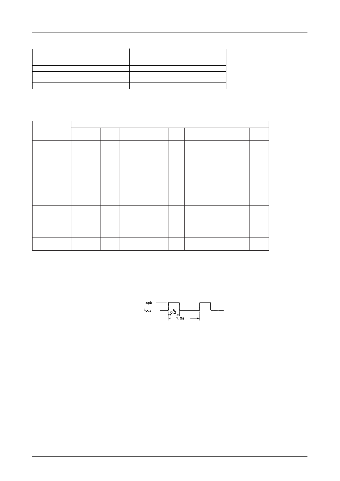
5 Peak current setting time.
No.1773–2/13
Page 3

Equivalent Circuit
STK7560 Series
Equivalent Circuit Block Diagram and Pin Assignment
Sample Application Circuit 1 : Standard peripheral circuit
Note1 The N. C pin (pin 18) must not be used as a relay pin for other line, pin.
2 Pins connected inside the IC (6-7, 8-9, 10-11, 14-15, 16-17) must be also connected on the printed circuit board.
No.1773–3/13
Page 4

STK7560 Series
Sample Application Circuit 2 : 3 Outpus including a nagative output
The secondary winding provided in the 5V choke coil provides 2 functions of choke coil and transformer, eliminating
the need to use a center tap on the input transformer to make a negative power supply available. The 5V output needs a
load of approximately 0.5A.
Sample 5V choke coil (for –12V output)
epytGro,F,AepytJ
erocetirreF62-IE03-IE
paGmm5.0tmm5.0 ×2
1N
2N
snrutfo.oNT04T53
aideriWømm6.0ømm8.0
snrutfo.oNT021T501
aidediWømm3.0ømm3.0
Sample data of 3-pin regulator input voltage (coil output voltage)/A, F, or G type
Sample Application Circuit 3 : STK7561A : 3 outputs of 5V, 12V, –12V
No.1773–4/13
Page 5

STK7560 Series
Sample Application Circuit 4 : STK7563F : 3 outputs of 5V, 24V, –12V
Sample Application Circuit 5 : STK7561A :Power supply for MSX personal computer,
2-output simultaneous ON/OFF
Sample Overvoltage Protector
Overcurrent may cause great damege. Particulary, the circuit connected to microcomputer power supply (5V) may be
damaged.
Shown below is a method to prevent this damage.
Connect a zener diode in parallel with the load. Use a DHD (double heat sink) type zener diode whose zener voltage is
1 to 2V higher than supply voltage (5V).
Overvoltage exceeding the zener voltage is limited by the zener diode.
With no current limiting rersistor connected, overcurrent flows in the zener diode.
Then, zener diode is shorted, thus protecting the load.
No.1773–5/13
Page 6

STK7560 Series
‘High active’ setting of cutoff input
‘Low active’ setting of cutoff input can be changed to ‘High active’ setting as shown below.
Sample Printed Circuit Pattern
Standard peripheral circuit for Sample Application Circuit 1 (Cu-foiled area)
Precautions
· Make the large current-carrying lines thicker and shorter.
· Please high input capacitor C1 close to the input pin of the
IC.
· Place switching spike-reducing C6, C7 close to the IC pins.
· Connect GND of ferrite bead core to GND of input capacitor C1 to minimize the core, C1-related pattern loop area.
· Connect V SENSE GND (pin 12) to GND of current line
near the load.
· Connect GND of output capacitors C3, C4, C5, C8 near the
load not to oppose current flow.
· Connect pins connected inside the IC (pins 6, 7, etc.) also on
the printed circuit board.
· Do not use NC (pin 18) as a relay pin for otherline, pin.
Resons
→ To minimize voltage loss on the pattern
→ To minimize input ripple.
→ To reduce switching spike more effectively.
→ To reduce switching spike more effectively.
→ To improve load regulation characteristic of
output voltage.
→ To improve ripple characteristic.
→ To provent current from concentrating on pin.
No.1773–6/13
Page 7

STK7561 Characteristics
STK7560 Series
STK7562 Characteristics
No.1773–7/13
Page 8

STK7563 Characteristics
STK7560 Series
No.1773–8/13
Page 9

STK7565 Characteristics
STK7560 Series
Termal Design
Most power dissipation of STK7560 series-applied volage regulators is caused by power transistor PTr, f lywheel diode
FRD, choke coil, current detect resistor.
Power detect parts are PTr FRD for the IC system, and TR1, D3 for OUTPUT 1, and TR6, D4 for OUTPUT 2. The
relation between output current and power dissipation is shown below.
No.1773–9/13
Page 10

STK7560 Series
Assuming power dissipation in each element as follows :
PT1 for power transistor of OUTPUT 1
PF1 for FRD of OUTPUT 1
PT2 for power transistor of OUTPUT 2
PF2 for FRD of OUTPUT 2
Total power dissipation Pd in the IC and heat sink thermal resistance θca are :
Pd= (PT + PF1) + (PT2 + PF2) [W]
Tc – Ta
θca= [°C/W]
where Tc : Case temperature=105°C, Ta=Ambient temperature
Junction temperature in each element is :
Tj= Pd × θjc + Tc [°C]
Pd
No.1773–10/13
Page 11

STK7560 Series
where Tj max=150°C, Pd : Power dissipation PT1, PF1, PT2, PF2 in each element,
θjc=Junction-case thermal resistance in each element.
lamrehTfoelbaTecnatsiseR θ cj
.oNepyT
A0657KTS9.45.219.45.21
F0657KTS
G0657KTS
J0657KTS7.25.57.45.21
To dessipate heat satisfactorily, use a heat sink with thermal resistance θca meeting two temperature conditions of
Tc max=105°C, Tj max=105°C.
Since the actual thermal resistance of the heat sink
greatly depends on various conditions such as equipment layout or ventilation, allow an ample margin in
thermal design. Shown right is the relation between Al
heat sink area and thermal resistance. The Al surface
coated with black improves thermal characteristic,
lowering thermal resistance approximately 20% as
compared with the Al heat sink of the same area.
1TUPTUO2TUPTUO
1RT3D6RT4D
7.45.217.25.5
Description of Operation of Internal Blocks
[OSC]
External excitation type OSC circuit where the CMOS NAND
gate-used ring OSC is formed by the 2-stage NAND circuit,
delivering basic pulses. This circuit provides pulse width modulation where the frequency is constant and the duty only varies.
[PWM]
Pulse width modulation (PWM) is provided by differentiating the
output of NAND gate 2 using the differentiating circuit of time
constant CR as shown left and by applying the result to the input of
NAND gate 3.
The threshold voltage at the input of NAND gate 3 is approximately 1/2 of supply voltage VDD applied to the gate and the PWM
output as shown below is obtained.
No.1773–11/13
Page 12

STK7560 Series
In the actual circuit transistor TR is connected in parallel with resistor R as
shown left. The error signal from the constant-voltage output side is used to
control the base current of TR so that the resistor value is varied equivalently to make the output voltage constant.
When the error signal is large, the base bias of TR is deepend and the
equivalent resistance gets small, narrowing the pulse width to control the
output voltage.
When the error signal is small, the base bias of TR is shallowed, widening
the pulse width to control the output voltage.
[OCP]
Overcurrent protection (OSC) is provided as follows : The voltage drop
across current detect resistor Rs of the external connection circuit is
detected to turn ON transistor TR1. Then, the collector current is
applied to the base of TR2 to make time constant CR small, forcing the
pulse width to be narrow.
The “fold-back” overcurrent characteristic occurs in which the pulse
width is narrowd to drop the output voltage and also to decrease the
output current.
[Cutoff]
The cutoff circuit (remote ON/OFF control) is so designed that the output is turned ON at ‘H’ level of cutoff input.
In the circuit shown below, when the input is at ‘H’ level, TR1 is turned ON to drop the base voltage of TR2 and
TR2 is turned OFF. Since TR2 is independent of the differentiating circuit composed of C and R, the output is
turned ON.
When the input is at ‘L’ level, TR1 is turned OFF to increase the base
voltage of TR2 and TR2 is turned ON. Since TR2 is connected in parallel
with R of the differentiating circuit, R is short-circuited to make R of time
constant CR O equivalently and the output is turned OFF.
New products = Development of 5V-1A rated small-sized STK7570 series
seireS
pueniL
.oNepyT
A1757KTS
B1757KTS
A2757KTS
B2757KTS
A3757KTS
B3757KTS
B5757KTS
B5757KTS
Maximum Ratings / Ta=25°C
xamniVxamcTgtsToVvaoIkpoIoVvaoIkpoI
)cdv()V()A()A()V()A()A(
05
]52[
05
]03[
06
]53[
07
]54[
(˚C) (˚C)
501
501
501
501
ot03–
501+
ot03–
501+
ot03–
501+
ot03–
501+
V1.0±V5
V1.0±V5
V1.0±V5
V1.0±V5
1TUPTUO2TUPTUO
1
1
1
1
1
1
1
1
2.1
2.1
2.1
2.1
2.1
2.1
2.1
2.1
2
V2.0±V21
3
2
V3.0±V51
3
2
V4.0±V42
3
2
V6.0±V63
3
4
6
4
6
4
6
4
6
No.1773–12/13
Page 13

STK7560 Series
Specifications of any and all SANYO products described or contained herein stipulate the performance,
characteristics, and functions of the described products in the independent state, and are not guarantees
of the performance, characteristics, and functions of the described products as mounted in the customer's
products or equipment. To verify symptoms and states that cannot be evaluated in an independent device,
the customer should always evaluate and test devices mounted in the customer's products or equipment.
SANYO Electric Co., Ltd. strives to supply high-quality high-reliability products. However, any and all
semiconductor products fail with some probability. It is possible that these probabilistic failures could
give rise to accidents or events that could endanger human lives, that could give rise to smoke or fire,
or that could cause damage to other property. When designing equipment, adopt safety measures so
that these kinds of accidents or events cannot occur. Such measures include but are not limited to protective
circuits and error prevention circuits for safe design, redundant design, and structural design.
In the event that any or all SANYO products(including technical data,services) described or
contained herein are controlled under any of applicable local export control laws and regulations,
such products must not be exported without obtaining the export license from the authorities
concerned in accordance with the above law.
No part of this publication may be reproduced or transmitted in any form or by any means, electronic or
mechanical, including photocopying and recording, or any information storage or retrieval system,
or otherwise, without the prior written permission of SANYO Electric Co. , Ltd.
Any and all information described or contained herein are subject to change without notice due to
product/technology improvement, etc. When designing equipment, refer to the "Delivery Specification"
for the SANYO product that you intend to use.
Information (including circuit diagrams and circuit parameters) herein is for example only ; it is not
guaranteed for volume production. SANYO believes information herein is accurate and reliable, but
no guarantees are made or implied regarding its use or any infringements of intellectual property rights
or other rights of third parties.
This catalog provides information as of November, 1999. Specifications and information herein are subject
to change without notice.
PS No.1773–13/13
 Loading...