

Page 1
Ordering number : ENN4421
92099RM (OT)/31293YO 5-3108 No. 4421-1/9
Overview
These days, the variety of horizontal frequencies output
from personal computers (PCs) include 15 kHz, 24 kHz,
31 kHz and even 33 kHz. These differences are dependent
on the device and maker, and the market itself contains
many PCs and a wide array of frequencies; in other word,
the need to remain compatible is stronger then ever. As
the number of video signal formats created with newmedia devices becomes more diversified, the search for
circuit technology capable of supporting such a wide
range of scanning frequencies (multiscan support)
becomes even harder.
The STK750-010 is a chopper regulator using MOS FET
with multi-scan support. This IC is also designed for
output voltage variable control supporting a wide range of
horizontal frequencies. For these reasons, the STK750010 helps reduce streamlined power supply designs,
shorten overall development time, and reduce total costs
while providing high-precision CRT display performance
with the highest quality.
Applications
• Multi-scan supporting CRT displays (secondary voltage
variable regulator)
Features
• High efficiency (97%) provided by power MOS FET.
Compared with bi-polar chopper regulators used until
now, power dissipation is less than half while supporting
compact heat sink and lighter weight design.
• Multi-scan support (output voltage variability).
Supports horizontal frequency external control.
• Wider output voltage control range (50 to 130 V),
compared with dropper type ICs used until now. The
resonance condenser changeover circuit and the vertical
dummy coil changeover circuit of horizontal deflection
coil are eliminated within the horizontal autoscan
circuit.
• IC operating frequency supports horizontal frequency
synchronization.
• Standard chopper type eliminates need for complicated
transformers and supports choke coil applications.
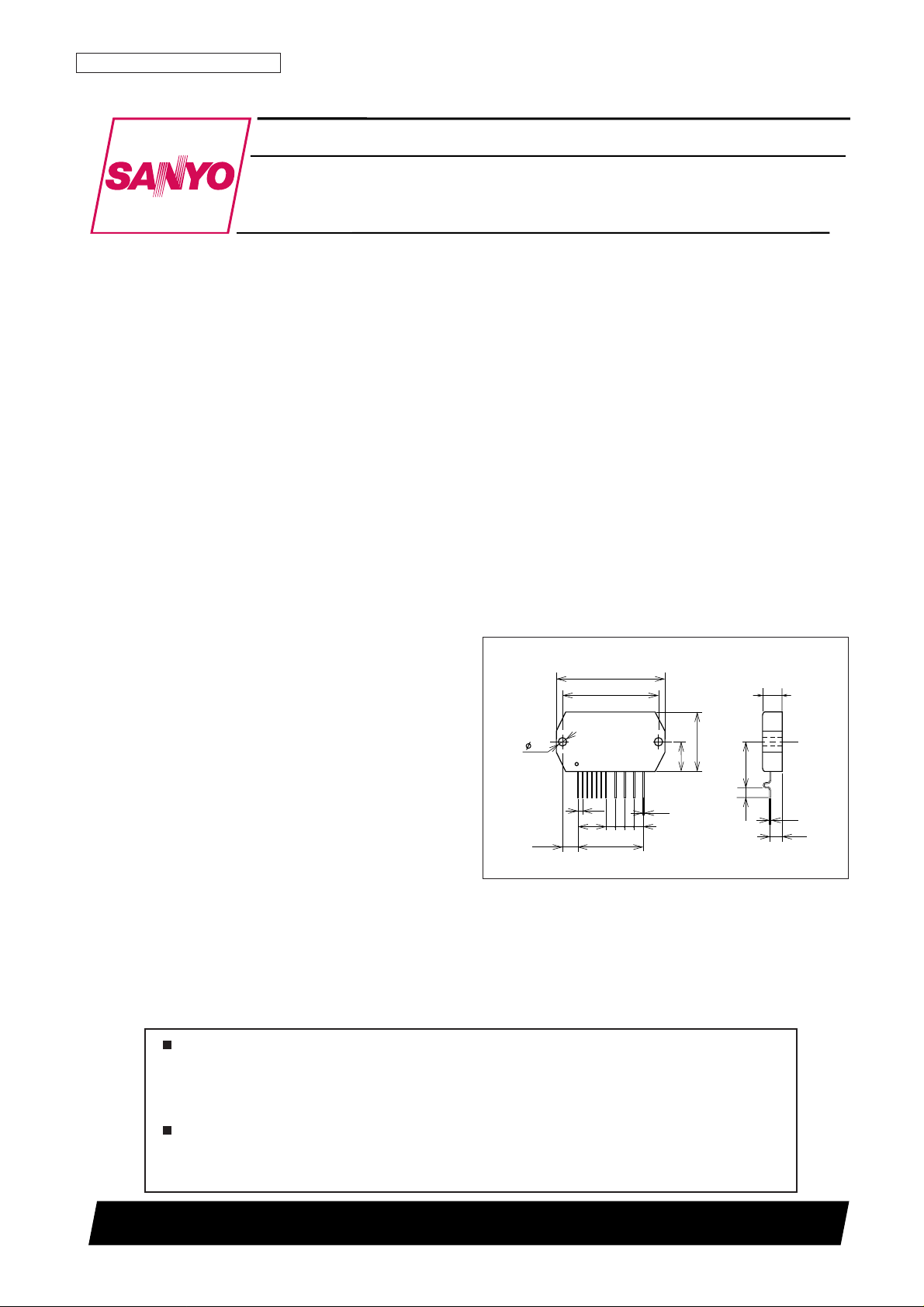
Package Dimensions
unit: mm
4136
115
46.6
41.2
12.7
25.5
(6.6)
2.0
×
14 = 28.0
0.5
2.0
12.0
8.5
0.4
5.2
4.0 20.0
AAAA
A = 4.0
3.6
[STK750-010]
STK750-010
SANYO Electric Co.,Ltd. Semiconductor Company
TOKYO OFFICE Tokyo Bldg., 1-10, 1 Chome, Ueno, Taito-ku, TOKYO, 110-8534 JAPAN
Chopper Regulator using MOS FET with Multi-Scan
Support (1 A Output Current)
Thick Film Hybrid IC
Any and all SANYO products described or contained herein do not have specifications that can handle
applications that require extremely high levels of reliability, such as life-support systems, aircraft’s
control systems, or other applications whose failure can be reasonably expected to result in serious
physical and/or material damage. Consult with your SANYO representative nearest you before using
any SANYO products described or contained herein in such applications.
SANYO assumes no responsibility for equipment failures that result from using products at values that
exceed, even momentarily, rated values (such as maximum ratings, operating condition ranges, or other
parameters) listed in products specifications of any and all SANYO products described or contained
herein.
Page 2
No. 4421-2/9
STK750-010
Parameter Symbol Conditions Ratings Unit
Maximum DC input voltage Vin (DC) max 190 V
Maximum output current Io max 1 A
Thermal resistance θj-c 2.5 °C/W
Junction temperature Tj max 150 °C
Operating substrate temperature Tc max 105 °C
Storage temperature Tstg –30 to +105 °C
Specifications
Maximum Ratings at Ta = 25°C
Parameter Symbol Conditions Ratings Unit
V
IN
voltage Vin 165 to 175 V
V
CC
voltage V
CC
11 to 13 V
Error amplifier input voltage Vamp 7 pin –0.3 to V
CC
–2 V
Timing condenser G
T
4 pin 0.47 to 10000 nF
Timing resistor R
T
3 pin 1.8 to 500 kΩ
Oscillation frequency f
OSC
20 to 100 kHz
Maximum duty D max 90 %
Recommended Operating Conditions at Ta = 25°C
Parameter Symbol Conditions
Ratings
Unit
min typ max
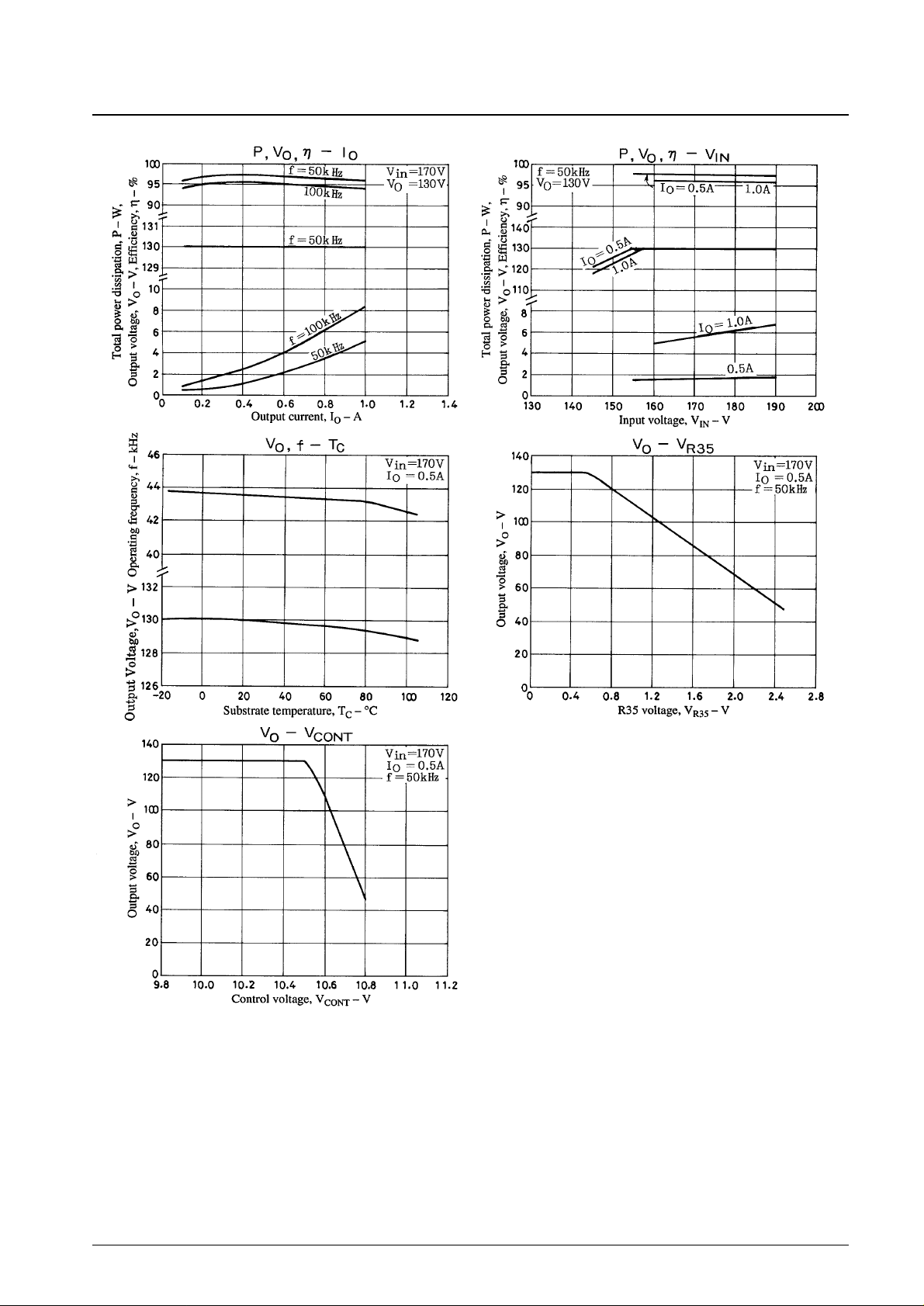
Output voltage Vo Vin (DC) = 170V, Io = 0.5A 130±1.5 V
Input regulaton Reg-IN Vin (DC) = 160 to 180V, Io = 0.5A 0.05 V/V
Load regulation Reg-L Vin (DC) = 170V, Io = 0.2 to 1A 0.5 V/A
Efficiency η Vin (DC) = 170V, Io = 0.5A 97 %
Output voltage temperature coefficient T
CVO
Vin (DC) = 170V, Io = 0.5A 17 mV/°C
Operating Characteristics at Ta = 25°C, see specified Test Circuit, f = 50kHz
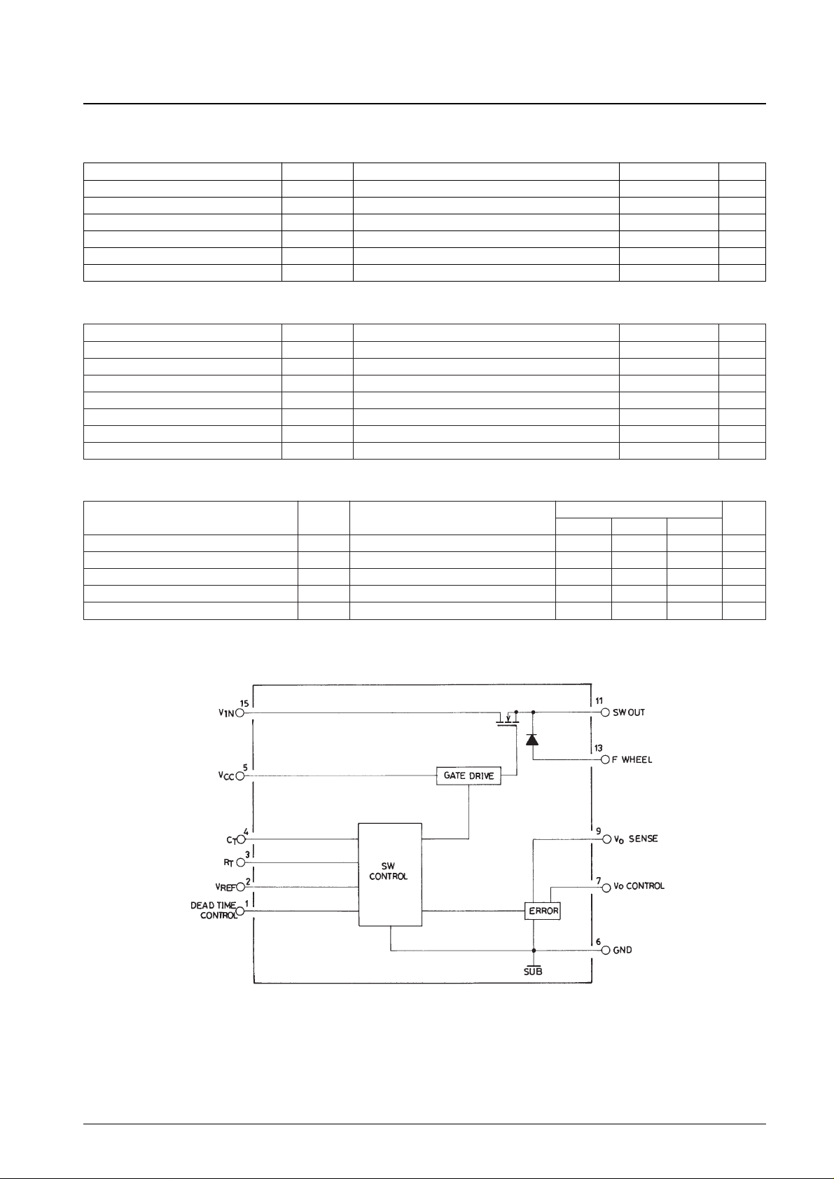
Block Diagram
Page 3
No. 4421-3/9
STK750-010
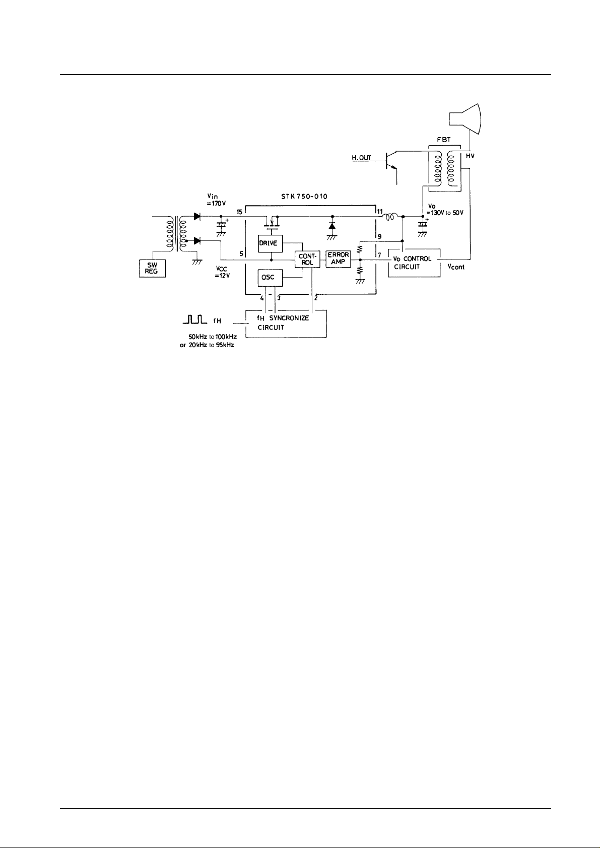
Application Circuit Block Diagram
Page 4

Test Circuit
C1 220µF / 200V R11 130KΩ TR11 2SC2274F L1 4.8mH
C2 220µF / 200V R12 8.2kΩ TR21 2SA984F
C3 10µF / 25V R13 470kΩ TR22 2SC2274F
C4 0.047µF / 250V R14 10kΩ TR31 2SA1209S
C11 22µF / 25V R21 2.0kΩ TR32 2SC2911S
C21 2200pF R22 47kΩ
C22 4700pF R23 30kΩ
C31 22µF / 25V R24 1kΩ IC31 LA6358
C32 10µF / 50V (N. P.) R25 100kΩ
C33 10µF / 25V R31 56kΩ
R32 100kΩ D21 GMA01
R33 3.9kΩ D31 GMA01
R34 10kΩ
R35 1kΩ
R36 100kΩ ZD31 GZA5.6X
R37 4.7kΩ
R38 4.7kΩ
R39 100Ω
R40 330kΩ
R41 10kΩ
VR31 500kΩ
No. 4421-4/9
STK750-010
Page 5

Description of Circuit Operations
1. Reference Voltage Circuit (REF REG.)
Reference voltage outputs at 5 V with built-in oscillator and protection circuits.
2. Oscillator (OSC)
When C and R are externally connected, self-oscillation of saw-tooth-wave forms begins. Charge current flows
from the CT pin (pin 4) to the condenser and when the CT pin reaches approximately 3 V, the discharge transistor
switches on and CT pin voltage drops to zero and one cycle ends. Charge current is determined by the current
flowing to the external resistor connected to the RT pin (pin 3).
Oscillation frequency is determined approximately according to the following equation:
f =
1.2
[kHz]
CT·R
T
CT: µF
RT: kΩ
3. Error Amplifier
Because the power supply error amplifier is supplied directly from VCC, the common mode input voltage range is
between –0.3 V and VCC–2 V. Figure 1 illustrates the equivalent circuit.
When output voltage is set to Vo, approximations are determined using the following equation:
Vo = V
REF’
x
R11 + R12
V
REF’
= 2.5V
R12
No. 4421-5/9
STK750-010
Oscillation frequency, f
OSC
– kHz
Figure 1
Page 6

Supported Functions
1. Oscillation Circuit
When all devices are synchronized to the clock cycle, a circuit diagram similar to that shown in figure 2 can be
synchronized.
2. Dead-time Adjustment Circuit (DT Pin)
Soft Start Circuit
R11 and R12 are dead-time setting resistors and vary DC input voltage. By modifying the slice level of the sawtooth wave, output maximum duty (on time) can be set. Maximum duty value should be set for approximately 90%.
If IC output pulse is operated at maximum duty when the power is turned on, a rush current flows to the output
transistor. Therefore, the duty cycle should be slowly increased from 0 (this is generally referred to as a “soft
start”). As shown in figure 3, configuration with the addition of a decay time constant circuit is possible using a
condenser connected to the dead-time control pin (1 pin).
Item R21 R22 f
OSC
External Synchronization Support Range f
H
EX1 2.4k 39k 45kHz 48k to 100kHz
EX2 3.3k 47k 37kHz 39k to 81kHz
EX3 4.3k 68k 28kHz 29k to 65kHz
EX4 5.1k 120k 18kHz 19k to 56kHz
No. 4421-6/9
STK750-010
Figure 2
Unit (resistance: Ω, capacitance: F)
Figure 3
Page 7
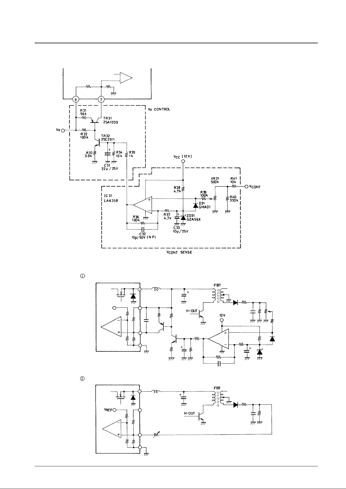
3. Output Voltage Vo Control Circuit
By supporting control voltage changes externally, output voltage Vo can be modified.
No. 4421-7/9
STK750-010
Unit (resistance: Ω, capacitance: F)
4. Support for Multi-Scan Applications
Page 8
No. 4421-8/9
STK750-010
Page 9

PS No. 4421-9/9
STK750-010
This catalog provides information as of September, 1999. Specifications and information herein are
subject to change without notice.
Specifications of any and all SANYO products described or contained herein stipulate the performance,
characteristics, and functions of the described products in the independent state, and are not guarantees
of the performance, characteristics, and functions of the described products as mounted in the customer’s
products or equipment. To verify symptoms and states that cannot be evaluated in an independent device,
the customer should always evaluate and test devices mounted in the customer’s products or equipment.
SANYO Electric Co., Ltd. strives to supply high-quality high-reliability products. However, any and all
semiconductor products fail with some probability. It is possible that these probabilistic failures could
give rise to accidents or events that could endanger human lives, that could give rise to smoke or fire,
or that could cause damage to other property. When designing equipment, adopt safety measures so
that these kinds of accidents or events cannot occur. Such measures include but are not limited to protective
circuits and error prevention circuits for safe design, redundant design, and structural design.
In the event that any or all SANYO products (including technical data, services) described or contained
herein are controlled under any of applicable local export control laws and regulations, such products must
not be exported without obtaining the export license from the authorities concerned in accordance with the
above law.
No part of this publication may be reproduced or transmitted in any form or by any means, electronic or
mechanical, including photocopying and recording, or any information storage or retrieval system,
or otherwise, without the prior written permission of SANYO Electric Co., Ltd.
Any and all information described or contained herein are subject to change without notice due to
product/technology improvement, etc. When designing equipment, refer to the “Delivery Specification”
for the SANYO product that you intend to use.
Information (including circuit diagrams and circuit parameters) herein is for example only; it is not
guaranteed for volume production. SANYO believes information herein is accurate and reliable, but
no guarantees are made or implied regarding its use or any infringements of intellectual property rights
or other rights of third parties.
 Loading...