

Page 1
Ordering number : EN6042
12299RM(OT) No. 6042-1/9
Overview
The STK672-120 is a unipolar fixed-current chopper type
2-phase stepping motor driver hybrid IC. It features power
MOSFETs in the output stage and a built-in phase signal
distribution IC. The incorporation of a phase distribution
IC allows the STK672-120 to control the speed of the
motor based on the frequency of an external input clock
signal. It supports two types of excitation for motor
control: 2-phase excitation and 1-2 phase excitation. It
also provides a function for switching the motor direction.
Applications
• Two-phase stepping motor drive in send/receive
facsimile units
• Paper feed in copiers, industrial robots, and other
applications that require 2-phase stepping motor drive
Features
• The motor speed can be controlled by the frequency of
an external clock signal (the CLOCK pin signal).
• The excitation type is switched according to the state
(low or high) of the MODE pin. The mode is set to
2-phase or 1-2 phase excitation on the rising edge of the
clock signal.
• A motor direction switching pin (the CWB pin) is
provided.
• All input are Schmitt inputs and 40-kΩ (typical: –50 to
+100%) pull-up resistors are built in.
• The motor current can be set by changing the Vref pin
voltage. Since a 0.165-Ω current detection resistor is
built in, a current of 1 A is set for each 0.165 V of
applied voltage.
• The input frequency range for the clock signal used for
motor speed control is 0 to 25 kHz.
• Supply voltage ranges: VCC1 = 10 to 42 V, VCC2 =
5.0 V ±5%
• This IC supports motor operating currents of up to 2.4 A
at Tc = 105°C, and of up to 4.0 A at Tc = 25°C.
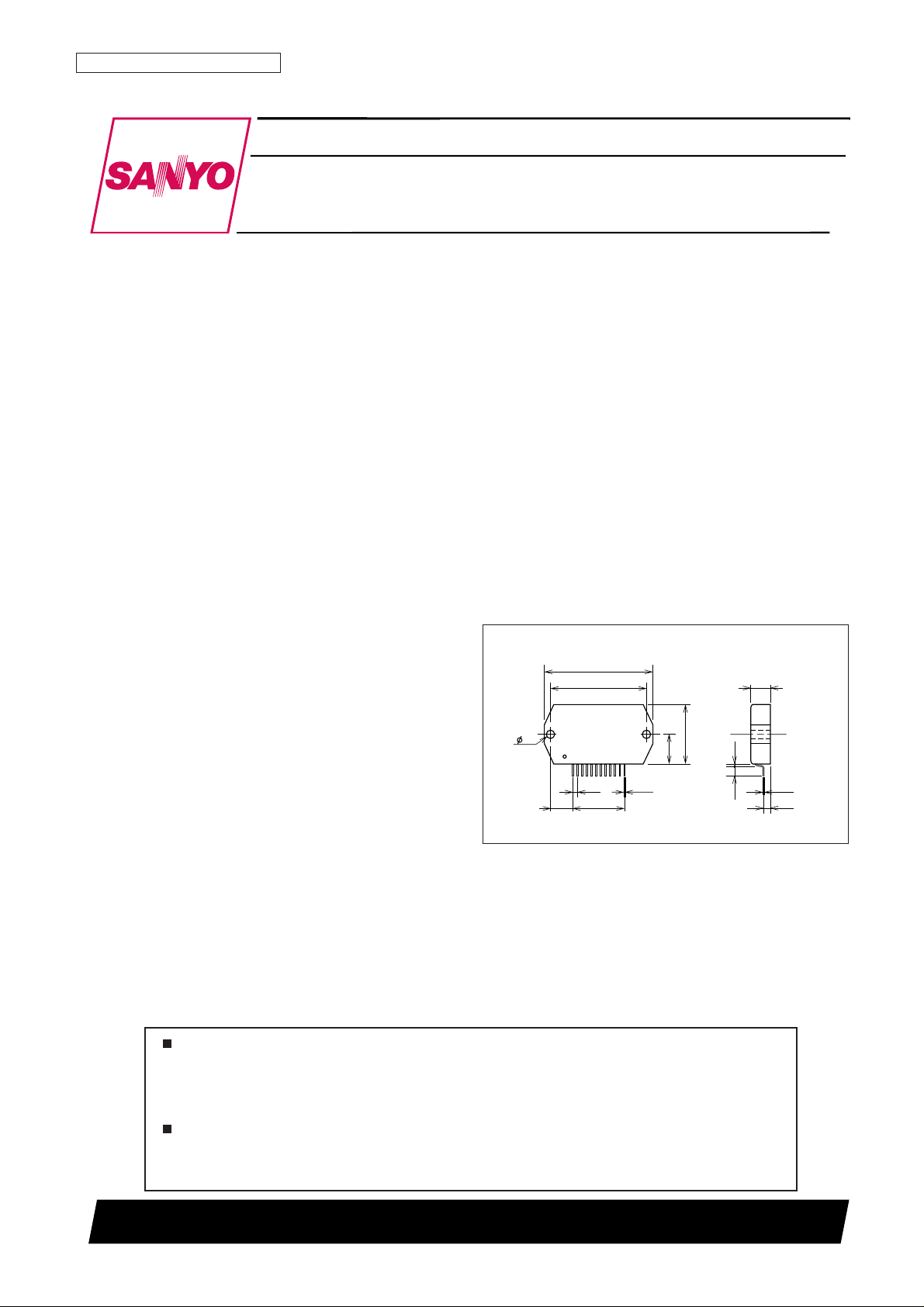
Package Dimensions
unit: mm
4167
1
12
46.6
41.2
12.7
25.5
(9.6)
11
×
2 = 22
3.6
0.5
2.0
8.5
4.0
0.4
2.9
1.0
[STK672-120]
STK672-120
SANYO Electric Co.,Ltd. Semiconductor Bussiness Headquarters
TOKYO OFFICE Tokyo Bldg., 1-10, 1 Chome, Ueno, Taito-ku, TOKYO, 110-8534 JAPAN
Unipolar Fixed-Current Chopper (Self-Excited PWM) Scheme and Built-in Phase Signal Distribution IC
Two-Phase Stepping Motor Driver
(Square Wave Drive) Output Current: 2.4 A
Thick-Film Hybrid IC
Any and all SANYO products described or contained herein do not have specifications that can handle
applications that require extremely high levels of reliability, such as life-support systems, aircraft’s
control systems, or other applications whose failure can be reasonably expected to result in serious
physical and/or material damage. Consult with your SANYO representative nearest you before using
any SANYO products described or contained herein in such applications.
SANYO assumes no responsibility for equipment failures that result from using products at values that
exceed, even momentarily, rated values (such as maximum ratings, operating condition ranges, or other
parameters) listed in products specifications of any and all SANYO products described or contained
herein.
Page 2
No. 6042-2/9
STK672-120
Parameter Symbol Conditions Ratings Unit
Maximum supply voltage 1 V
CC
max No signal 52 V
Maximum supply voltage 2 V
DD
max No signal –0.3 to +7.0 V
Input voltage V
IN
max Logic input pins –0.3 to +7.0 V
Output current I
OH
max VDD= 5 V, CLOCK ≥ 200 Hz 4.0 A
Repeated avalanche capacity Ear max 36 mJ
Allowable power dissipation Pd max With an arbitrarily large heat sink. Per MOSFET 8.5 W
Operating substrate temperature Tc max 105 °C
Junction temperature Tj max 150 °C
Storage temperature Tstg –40 to +125 °C
Specifications
Maximum Rating at Ta = 25°C
Parameter Symbol Conditions Ratings Unit
Maximum supply voltage 1 V
CC
With signals applied 10 to 42 V
Maximum supply voltage 2 V
DD
With signals applied 5.0 ± 5% V
Input voltage V
IH
0 to V
DD
V
Phase current 1 I
OH
1 Tc = 105°C, CLOCK ≥ 200 Hz 2.4 A
Phase current 2 I
OH
2
Tc = 80°C, CLOCK ≥ 200 Hz
3.0 A
See the motor current (I
OH
) derating curve
Clock frequency f
CL
Minimum pulse width: 20 µs 0 to 25 kHz
Phase driver withstand voltage V
DSSID
= 1 mA (Tc = 25°C) 100 min V
Allowable Operating Ranges at Ta = 25°C
Parameter Symbol Conditions
Ratings
Unit
min typ max
V
DD
supply current I
CCO
CLOCK = GND 2.6 6 mA
Output current I
oave
With R/L = 3 Ω/3.8 mH in each phase
0.56 0.62 0.69 A
Vref = 0.176 V
FET diode forward voltage Vdf If = 1 A (R
L
= 23 Ω) 1.1 1.7 V
Output saturation voltage Vsat R
L
= 23 Ω 0.40 0.56 V
High-level input voltage V
IH
Pins 6 to 9 (4 pins) 4.0 V
Low-level input voltage V
IL
Pins 6 to 9 (4 pins) 1.0 V
Input current I
IL
With pins 6 to 9 at the ground level.
62 125 250 µA
Pull-up resistance: 40 kΩ (typical)
Vref input voltage VrH Pin 12 0 3.5 V
Vref input bias current I
IB
With pin 12 at 1 V 50 500 nA
Electrical Characteristics at Ta = 25°C, VCC= 24 V, VDD= 5 V
Note: A fixed-voltage power supply must be used.
Page 3
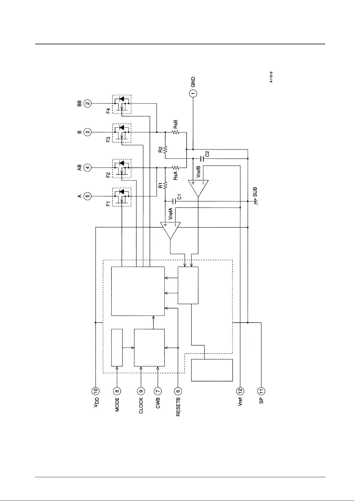
Internal Equivalent Circuit Block Diagram
No. 6042-3/9
STK672-120
Phase excitation signal
generation
Chopping circuit
Off time
setting
Phase advance
counter
Excitation mode
selection
Page 4

Sample Application Circuit
• To minimize noise in the 5-V system, locate the ground side of capacitor CO2 in the above circuit as close as possible
to pin 1 of the IC.
• Insert resistor RO3 (47 to 100 Ω) so that the discharge energy from capacitor CO4 is not directly applied to the CMOS IC
in this hybrid device. If the diode D1 has Vf characteristics with Vf less than or equal to 0.6 V (when If = 0.1 A), this will
be smaller than the CMOS IC input pin diode Vf. If this is the case RO3 may be replaced with a short without problem.
• Standard or HC type input levels are used for the pin 7, 8, and 9 inputs.
• If open-collector type circuits are used for the pin 7, 8, and 9 inputs, these circuit will be in the high-impedance state
for high level inputs. As a result, chopping circuit noise may cause the input circuits to operate incorrectly. To prevent
incorrect operation due to such noise, capacitors with values between 470 and 1000 pF must be connected between pins
7 and 11, 8 and 11, and 9 and 11. (A capacitor with a value between 470 and 1000 pF must be connected between pins
6 and 11 as well if an open-collector output IC is used for the RESETB pin (pin 6) input.)
• Taking the input bias current (IIB) characteristics into account, the resistor RO1 must not exceed 100 kΩ.
• The following circuit (for a lowered current of over 0.2 A) is recommended if the application needs to temporarily
lower the motor current. Here, a value of close to 100 kΩ must be used for resistor RO1 to make the transistor output
saturation voltage as low as possible.
No. 6042-4/9
STK672-120
Input Pin Functions (CMOS input levels)
Pin Pin No. Function Input conditions when operating
CLOCK 9 Reference clock for motor phase current switching Operates on the rising edge of the signal
MODE 8 Excitation mode selection
Low: 2-phase excitation
High: 1-2 phase excitation
CWB 7 Motor direction switching
Low: CW (forward)
High: CCW (reverse)
RESETB 6
System reset and A, AB, B, and BB outputs cutoff.
A reset is applied by a low level
Applications must apply a reset signal for at least 20 µs when power is first applied.
• A simple reset function is formed from D1, CO4, and RO3 in this application circuit. With the CLOCK input held low,
when the 5-V supply voltage is brought up a reset is applied if the motor output phases A and BB are driven. If the 5-V
supply voltage rise time is slow (over 50 ms), the motor output phases A and BB may not be driven. Increase the value
of the capacitor CO4 and check circuit operation again.
• See the timing chart for the specific details on circuit operation.
Two-phase stepping motor
At least 100 µF
Page 5

Usage Notes
• 5-V system input pins
[RESETB and CLOCK (Input signal timing when power is first applied)]
As shown in the timing chart, a RESETB signal input is required by the driver to operate with the timing in which the F1
gate is turned on first. The RESETB signal timing must be set up to have a width of at least 20 µs, as shown below.
The capacitor CO4 and the resistor RO3 in the application circuit form simple reset circuit that uses the RC time
constant rising time. However, when designing the RESETB input based on CMOS levels, the application must have
the timing shown in figure 1.
Figure 1 RESETB and CLOCK Signals Input Timing
No. 6042-5/9
STK672-120
See the timing chart for details on the CLOCK, MODE, CWB, and other input pins.
[Vref <Motor current peak value setting>]
In the sample application circuit, the peak value of the motor current (IO) is set by RO1, RO2, and VDD(5 V) as
described by the formula below.
IOH= Vref ÷ Rs Here, Rs is hybrid IC internal current detection resistor
Vref = (R02 ÷ (R01 + R02)) × 5 V
STK672-120 : Rs = 0.165 Ω
• Allowable motor current operating range
The motor current (IO) must be held within the range corresponding to the area under the curve shown in figure 4.
For example, if the operating substrate temperature Tc is 105°C, then IOmust be held under IOmax = 2.4 A, and in
hold mode IOmust be held under IOmax = 2.0 A.
Figure 2 Motor Current IOFlowing into the Driver IC
Rise of the 5-V supply voltage
RESETB signal input
CLOCK signal
At least 20 µs
At least 10 µs
Page 6

• Thermal design
[Operating range in which a heat sink is not used]
Thermal design that lowers this hybrid IC’s operating substrate temperature can be effective in improving end product
quality. The size of the heat sink required by this hybrid IC varies with the average power dissipation PD. The value of
PDincreases as the output current increases, as shown in figure 5.
Since there are periods when current flows and periods when the current is off during actual motor operation, P
D
cannot be determined from the data presented in figure 5. Therefore, we calculate PDassuming that actual motor
operation consists of repetitions of the operation shown in figure 3.
No. 6042-6/9
STK672-120
Figure 3 Motor Current Timing
T1: Motor rotation operation time
T2: Motor hold operation time
T3: Motor current off time
T2 may be reduced, depending on the application.
T0: Single repeated motor operating cycle
IO1 and IO2: Motor current peak values
Due to the structure of motor windings, the phase current is a positive and negative current with a pulse form.
Note that figure 3 presents the concepts here, and that the on/off duty of the actual signals will differ.
The hybrid IC internal average power dissipation PDcan be calculated from the following formula.
PD= (T1 × P1 + T2 × P2 + T3) ÷ T0 (I)
(Here, P1 is the PDfor IO1 and P2 is the PDfor IO2)
If the value calculated in formula (I) above is under 1.5 W, then there will be no need to use a heat sink for ambient
temperatures Ta up to 60°C. See figure 6 for operating substrate temperature rise data when a heat sink is not attached.
If a heat sink is to be used, to lower Tc if PDincreases, use formula (II) and the graph in figure 7 to determine the size of
the heat sink.
θ
c - a = (Tc max–Ta) ÷ PD (II)
Tcmax: Maximum operating substrate temperature = 105°C
Ta: The hybrid IC ambient temperature
While formulas (I) and (II) above are adequate for thermal design, note that figure 5 is merely a single example of one
operating mode for a single motor. For example, while figure 5 shows a 2-phase excitation motor, if 1-2 phase excitation
is used with a 500-Hz clock frequency, the drive will be turned off for 25% of the time and the loss PDwill be reduced to
75% of that in figure 5.
It is extremely difficult for Sanyo to calculate the internal average power dissipation PDfor all possible end product
conditions. After performing the above rough calculations, always install the hybrid IC in an actual end product and
verify that the substrate temperature Tc does not rise above 105°C.
Motor phase current
(sink side)
Page 7

Timing Chart
No. 6042-7/9
STK672-120
2-phase excitation
Gate F1
Gate F2
Gate F3
Gate F4
Gate F1
Gate F2
Gate F3
Gate F4
1-2 phase excitation
Page 8

No. 6042-8/9
STK672-120
1-2 phase excitation (CWB)
Gate F1
Gate F2
Gate F3
Gate F4
Gate F1
Gate F2
Gate F3
Gate F4
Switching from 2-phase to 1-2 phase excitation
Page 9

PS No. 6042-9/9
STK672-120
This catalog provides information as of January, 1999. Specifications and information herein are subject
to change without notice.
Specifications of any and all SANYO products described or contained herein stipulate the performance,
characteristics, and functions of the described products in the independent state, and are not guarantees
of the performance, characteristics, and functions of the described products as mounted in the customer’s
products or equipment. To verify symptoms and states that cannot be evaluated in an independent device,
the customer should always evaluate and test devices mounted in the customer’s products or equipment.
SANYO Electric Co., Ltd. strives to supply high-quality high-reliability products. However, any and all
semiconductor products fail with some probability. It is possible that these probabilistic failures could
give rise to accidents or events that could endanger human lives, that could give rise to smoke or fire,
or that could cause damage to other property. When designing equipment, adopt safety measures so
that these kinds of accidents or events cannot occur. Such measures include but are not limited to protective
circuits and error prevention circuits for safe design, redundant design, and structural design.
In the event that any or all SANYO products (including technical data, services) described or contained
herein are controlled under any of applicable local export control laws and regulations, such products must
not be exported without obtaining the export license from the authorities concerned in accordance with the
above law.
No part of this publication may be reproduced or transmitted in any form or by any means, electronic or
mechanical, including photocopying and recording, or any information storage or retrieval system,
or otherwise, without the prior written permission of SANYO Electric Co., Ltd.
Any and all information described or contained herein are subject to change without notice due to
product/technology improvement, etc. When designing equipment, refer to the “Delivery Specification”
for the SANYO product that you intend to use.
Information (including circuit diagrams and circuit parameters) herein is for example only; it is not
guaranteed for volume production. SANYO believes information herein is accurate and reliable, but
no guarantees are made or implied regarding its use or any infringements of intellectual property rights
or other rights of third parties.
Motor current, I
OH
— A
Substrate temperature rise, ∆T
C
— °C
Operating Substrate Temperature, TC— °C
With no heat sink, the IC
vertical, and convection cooling
With a black
surface finish
With no surface
finishing
Hybrid IC internal average power dissipation, PD— W
Hybrid IC internal average power dissipation, P
D
— W
Motor current, IOH— A
Heat sink thermal resistance,
θ
c–a — °C/W
Heat sink area, S — cm
2
Continuous 2-phase
excitation operation
Motor used:R = 0.63 Ω
L = 0.62 mH
The data are typical values.
Operating region when fCL≥ 200 Hz
Operating region in hold mode
Motor:
Figure 4
Figure 6 Figure 7
Figure 5
 Loading...