

Page 1
Ordering number : ENN5227B
60200RM (OT) No. 5227-1/19
Overview
The STK672-040 is a stepping motor driver hybrid IC that
uses power MOSFETs in the output stage. It includes a
built-in microstepping controller and is based on a
unipolar constant-current PWM system. The STK672-040
supports application simplification and standardization by
providing a built-in 4 phase distribution stepping motor
controller. It supports five excitation methods: 2 phase,
1-2 phase, W1-2 phase, 2W1-2 phase, and 4W1-2 phase
excitations, and can provide control of the basic stepping
angle of the stepping motor divided into 1/16 step units. It
also allows the motor speed to be controlled with only a
clock signal.
The use of this hybrid IC allows designers to implement
systems that provide high motor torques, low vibration
levels, low noise, fast response, and high-efficiency drive.
Compared to the earlier Sanyo STK672-010 Series, the
STK672-040 features a smaller package, fewer external
components, and controller improvements for even higher
efficiency and even higher performance microstepping
motor drive.
Applications
• Facsimile stepping motor drive (send and receive)
• Paper feed and optical system stepping motor drive in
copiers
• Laser printer drum drive
• Printer carriage stepping motor drive
• X-Y plotter pen drive
• Industrial robots and other stepping motor applications
Features
• Can implement stepping motor drive systems simply by
providing a DC power supply and a clock pulse
generator.
<Control Block Features>
• One of five drive types can be selected with the drive
mode settings (M1, M2, and M3)
—2 phase excitation drive
—1-2 phase excitation drive
—W1-2 phase excitation drive
—2W1-2 phase excitation drive
—4W1-2 phase excitation drive
• Provides four freely selectable modes for the vector
locus during microstepping drive: circular mode, one
inside mode, and two outside modes.
• Phase retention even if excitation is switched.
• The excitation phase state can be verified in real time
from the MO1, MO2, and MOI signal output pins.
• The CLK input counter block can be selected to be one
of the following by the high/low setting of the M3 input
pin.
—Rising edge only
—Both rising and falling edges
Note*: Conditions: VCC1 = 24 V, IOH= 1.5 A, 2W1-2 drive
used.
Continued on next page.
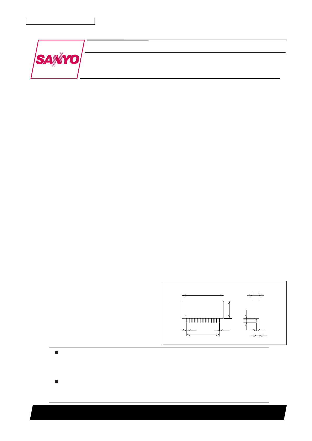
Package Dimensions
unit: mm
4161
122
53.0
21
×
2 = 42
0.5
2.0
22.0
9.0
0.4
2.9
4.0
1.0
[STK672-040]
STK672-040
SANYO Electric Co.,Ltd. Semiconductor Company
TOKYO OFFICE Tokyo Bldg., 1-10, 1 Chome, Ueno, Taito-ku, TOKYO, 110-8534 JAPAN
Stepping Motor Driver (Sine Wave Drive) Output Current: 1.5 A (No Heat Sink*)
Unipolar constant-current chopper (external excitation PWM) circuit with built-in microstepping controller
Thick-Film Hybrid IC
Any and all SANYO products described or contained herein do not have specifications that can handle
applications that require extremely high levels of reliability, such as life-support systems, aircraft’s
control systems, or other applications whose failure can be reasonably expected to result in serious
physical and/or material damage. Consult with your SANYO representative nearest you before using
any SANYO products described or contained herein in such applications.
SANYO assumes no responsibility for equipment failures that result from using products at values that
exceed, even momentarily, rated values (such as maximum ratings, operating condition ranges, or other
parameters) listed in products specifications of any and all SANYO products described or contained
herein.
Page 2
• The CLK and RETURN input pins include built-in
malfunction prevention circuits for external pulse noise.
• ENABLE and RESET pins provided. These are Schmitt
trigger inputs with built-in 20 kΩ (typical) pull-up
resistors.
• No noise generation due to the difference between the A
and B phase time constants during motor hold since
external excitation is used.
• Microstepping operation supported even for small motor
currents, since the reference voltage Vref can be set to
any value between 0 V and 1/2VCC2.
<Driver Block>
• External excitation PWM drive allows a wide operating
supply voltage range (VCC1 = 10 to 45 V) to be used.
• Current detection resistor (0.33 Ω) built into the hybrid
IC.
• Power MOSFETs for minimal driver loss
• Motor output drive currents IOHup to 1.5 A.
No. 5227-2/19
STK672-040
Parameter Symbol Conditions Ratings Unit
Maximum supply voltage 1 V
CC
1 max No signal 52 V
Maximum supply voltage 2 V
CC
2 max No signal –0.3 to +7.0 V
Input voltage V
IN
max Logic input pins –0.3 to +7.0 V
Phase output current I
OH
max
0.5 seconds, single pulse, with V
CC
1 applied.
2.2 A
Load: R = 5 Ω, L = 10 mH for each phase.
Repeatable avalanche Ear max 38 mJ
Power loss Pd max θc-a = 0 12 W
Operating temperature Tc max 105 °C
Junction temperature Tj max 150 °C
Storage temperature Tstg –40 to +125 °C
Specifications
Absolute Maximum Ratings at Ta = 25°C
Parameter Symbol Conditions Ratings Unit
Supply voltage 1 V
CC
1 With input signals present 10 to 45 V
Supply voltage 2 V
CC
2 With input signals present 5 ±5% V
Input voltage V
IH
0 to VCC2V
Phase driver voltage handling V
DSS
Tr1, 2, 3, and 4 (the A, A, B, and B outputs) 100 (min) V
Phase current I
OH
max Duty 50% 1.5 (max) A
Allowable Operating Ranges at Ta = 25°C
Parameter Symbol Conditions
Ratings
Unit
min typ max
Control supply current I
CC
Pin 7, with ENABLE pin held low. 4.5 15 mA
Output saturation voltage Vsat R
L
= 15 Ω (I ≈ 1.5 A) 1.4 1.9 V
Average output current Io ave
Load: R = 3.5 W/L = 3.8 mH
0.465 0.517 0.569 A
For each phase, Vref ≈ 1 V
FET diode forward voltage Vdf If = 1 A 1.2 1.8 V
[Control Inputs]
Input voltage
V
IH
Except for the Vref pin 4 V
V
IL
Except for the Vref pin 1 V
Input current
I
IH
Except for the Vref pin 0 1 10 µA
I
IL
Except for the Vref pin 125 250 510 µA
[Vref Input Pin]
Input voltage V
I
Pin 8 0 2.5 V
Input current I
I
Pin 8 1µA
[Control Outputs]
Output voltage
V
OH
I = –3 mA, pins MOI, MO1, MO2 2.4 V
V
OL
I = +3 mA, pins MOI, MO1, MO2 0.4 V
Electrical Characteristics at Tc = 25°C, VCC1 = 24 V, VCC2 = 5 V
Continued on next page.
Continued from preceding page.
Page 3

No. 5227-3/19
STK672-040
Parameter Symbol Conditions
Ratings
Unit
min typ max
[Current Distribution Ratio (A·B)]
2W1-2, W1-2, 1-2 Vref θ = 1/8 100 %
2W1-2, W1-2 Vref θ = 2/8 92 %
2W1-2 Vref θ = 3/8 83 %
2W1-2, W1-2, 1-2 Vref θ = 4/8 71 %
2W1-2 Vref θ = 5/8 55 %
2W1-2, W1-2 Vref θ = 6/8 40 %
2W1-2 Vref θ = 7/8 20 %
2 Vref 100 %
PWM frequency fc 37 47 57 kHz
Continued from preceding page.
Note: A constant-voltage power supply must be used.
The design target value is shown for the current distribution ratio.
Page 4
21
20
19
16
18
22
17
11
14
15
10
9
7 12 13 8 6 5 2 1
+
–
+
–
+
–
+
–
+
–
3
4
M1
M2
CWB
CLK
M3
RETURN
RESET
MoI
Mo1
Mo2
ENABLE
SG
SUB
PG
BBAAVrefM5M4V
CC
2
Excitation mode
control
Excitation state monitor
Phase
advance
counter
Current
distribution
ratio switching
Pseudo-sine
wave generator
Rise detection
RC oscillator PWM control
Reference clock
generation
Phase excitation drive
signal generation
Rise/fall
detection and switching
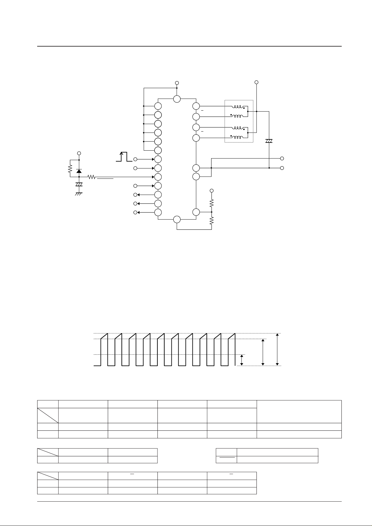
A12389
Internal Block Diagram
No. 5227-4/19
STK672-040
Page 5
Test Circuit Diagrams
No. 5227-5/19
STK672-040
14
9
10
8
16
22
3
4
1
2
5
6
A
15 Ω
A
B
B
7
+
VCC2
VCC2
STK672-040
Start
Vref = 2.5 V
V
22
3
4
1
2
5
6
A
A
B
B
7
VCC1
STK672-040
V
A
A12390
14
9
10
8
16
22
1
5
2
6
A
abab
A
B
SW2
SW1
B
7
18
+
VCC2
VCC2
VCC1
VCC1
STK672-040
Start
Vref = 1 V 0 V
0 V
Low when
measuring I
CC
5 V
A12393
9
22
7
A
VCC2
M1
STK672-040
A12392
A12391
10
M2
11
M3
12
M4
13
M5
14
CLK
14
1415
CWB
1416
RESET
1417
RETURN
1418
ENABLE
148
Vref
A
A
I
IL
I
IH
Vsat Vdf
IIH, I
IL
Ioave, Icc, fc
When measuring Io ave: With SW1 set to ‘a’, Vref = 1 V
When measuring fc: With SW1 set to ‘b’, Vref = 0 V
When measuring Icc: Set ENABLE low.
Page 6
No. 5227-6/19
STK672-040
9
22
8
6
A
A
7
141410
141411
141412
141413
141415
14
18
16
17
19
20
21
+
+
VCC2 = 5 V
VCC2 = 5 V
SG
100 µF or higher
PG
Vref
VCC2 = 5 V
1 kΩ
CLK
ENABLE
RET
RESET
MoI
Mo1
Mo2
VCC1 = 10 V to 45 V
Two-phase stepping motor
STK672-040
A12394
B
B
5
2
1
3
4
0 A
Motor current waveform
Ioave
A12395
IOLI
OH
Note: This hybrid IC must be initialized with a power on reset when power is first applied.
Operation Description
2W1-2 Phase Excitation Drive (microstepping operation)
[Setting the Motor Current]
The motor current IOHis set by the Vref voltage on the hybrid IC pin 8. The following formula gives the relationship
between IOHand Vref.
1
IOH=—× Vref/Rs, Rs: The hybrid IC internal current detection resistor (0.33 Ω ±3%)
3
Applications can use motor currents from the current (0.05 to 0.1 A) set by the duty of the frequency set by the oscillator
up to the limit of the allowable operating range, IOH= 1.5 A
[Function Table]
M20011
M1
0101
Phase switching clock edge timing
M3
1 2 phase excitation 1-2 phase excitation W1-2 phase excitation 2W1-2 phase excitation Rising edge only
0 1-2 phase excitation W1-2 phase excitation 2W1-2 phase excitation 4W1-2 phase excitation Rising and falling edges
Forward Reverse
CWB 0 1
AABB
Mo11001
Mo20011
ENABLE Motor current is cut off when low
RESET Active low
Page 7

Printed Circuit Board Design Recommendations
This hybrid IC has two grounds, the PG pins (pins 3 and 4) and the SG pin (pin 22). These are connected internally in the
hybrid IC.
Two power supplies are required: a motor drive supply and a 5 V supply for the hybrid IC itself. If the ground
connections for these supplies are not good, the motor current waveforms may become unstable, motor noise may
increase, and vibration levels may increase. Use appropriate wiring for these grounds. Here we present two methods for
implementing these ground connections.
If the grounds for the motor drive supply and the hybrid IC 5 V supply are connected in the immediate vicinity of the
power supplies:
• If PG and SG are shorted at the power supply, connect only the PG line to pins 3 and 4 on the hybrid IC. Also, be sure
that no problems occur due to voltage drops due to common impedances. In the specifications, this must be VCC2 ±5%.
• The current waveforms will be more stable if the Vref ground is connected to pin 22.
• For initial values, use 100 µF or over for C1 and 10 µF or over for C2.
Locate C1 as close to the hybrid IC as possible, and the capacitor ground line must be as short as possible.
No. 5227-7/19
STK672-040
+
+
Motor
drive
power
supply
5 V
power
supply
100 µF or over
C1
PG
SG
Stepping motor
C2
10 µF
or over
Oscillator
circuit
(CLK)
3
PG
4
22
14
SG
CLK
STK672-040
7 VCC2
8 Vref
A12396
Motor
drive
power
supply
5 V
power
supply
+
+
100 µF or over
Separation
C1
PG
SG
Stepping motor
C2
10 µF
or over
3
PG
4
22
14
SG
CLK
STK672-040
7 VCC2
8 Vref
A12397
Oscillator
circuit
(CLK)
If the grounds for the motor drive supply and the hybrid IC 5 V supply are separated:
• Insert a capacitor (C1) of 100 µF or over as close as possible to the hybrid IC. The capacitor ground line must be as
short as possible.
The capacitor C2 may be included if necessary. Its ground line should also be as short as possible.
Page 8

No. 5227-8/19
STK672-040
D1
Rs
L2
VCC1
I
OFF
L1
ØA ØA
MOSFET
AND
Q
S
R
800 kHz
45 kHz
Latch circuit
Noise
filter
CR
oscillator
Divider
Current
divider
M4 M5
Vref
A = 1
+
–
Enable ØA (control signal)
I
ON
A12398
Functional Description
External Excitation Chopper Drive Block Description
Since this hybrid IC adopts an external excitation method, no external oscillator circuit is required.
When a high level is input to øA in the basic driver block circuit shown in the figure and the MOSFET is turned on, the
comparator + input will go low and the comparator output will go low. Since a set signal with the PWM period will be
input, the Q output will go high, and the MOSFET will be turned on as its initial value.
The current IONflowing in the MOSFET passes through L1 and generates a potential difference in Rs. Then, when the Rs
potential and the Vref potential become the same, the comparator output will invert, and the reset signal Q output will
invert to the low level. Then, the MOSFET will be turned off and the energy stored in L1 will be induced in L2 and the
current I
OFF
will be regenerated to the power supply. This state will be maintained until the time when an input to the
latch circuit set pin occurs.
In this manner, the Q output is turned off and on repeatedly by the reset and set signals, thus implementing constant
current control. The resistor and capacitor on the comparator input are spike removal circuit elements and synchronize
with the PWM frequency. Since this hybrid IC uses a fixed frequency due to the external excitation method and at the
same time also adopts a synchronized PWM technique, it can suppress the noise associated with holding a position when
the motor is locked.
Driver Block Basic Circuit Structure
Input Pin Functions
Pin No. Symbol Function Pin circuit type
14 CLK Phase switching clock Built-in pull-up resistor CMOS Schmitt trigger input
15 CWB Rotation direction setting (CW/CCW) Built-in pull-up resistor CMOS Schmitt trigger input
17 RETURN Forced phase origin return Built-in pull-up resistor CMOS Schmitt trigger input
18 ENABLE Output cutoff Built-in pull-up resistor CMOS Schmitt trigger input
9, 10, 11 M1, M2, M3 Excitation mode setting Built-in pull-up resistor CMOS Schmitt trigger input
12, 13 M4, M5 Vector locus setting Built-in pull-up resistor CMOS Schmitt trigger input
16 RESET System reset Built-in pull-up resistor CMOS Schmitt trigger input
8 Vref Current setting Operational amplifier input
Page 9

Input Signal Functions and Timing
• CLK (phase switching clock)
Input frequency range: DC to 50 kHz
Minimum pulse width: 10 µs
Duty: 40 to 60% (However, the minimum pulse width takes precedence when M3 is high.)
Pin circuit type: Built-in pull-up resistor (20 kΩ, typical) CMOS Schmitt trigger structure
Built-in multi-stage noise rejection circuit
Function
—When M3 is high or open: The phase excited (driven) is advanced one step on each CLK rising edge.
—When M3 is low: The phase moves on both the rising and falling edges of the CLK signal, for a total of two steps
per cycle.
• CWB (Method for setting the rotation direction)
Pin circuit type: Built-in pull-up resistor (20 kΩ, typical) CMOS Schmitt trigger structure
Function
—When CWB is high: The motor turns in the clockwise direction.
—When CWB is low: The motor turns in the counterclockwise direction.
Notes: When M3 is low, the CWB input must not be changed for about 6.25 µs before or after a rising or falling edge
on the CLK input.
• RETURN (Forcible return to the origin for the currently excited phase)
Pin circuit type: Built-in pull-up resistor (20 kΩ, typical) CMOS Schmitt trigger structure
Built-in noise rejection circuit
Notes: The currently excited (driven) phase can be forcibly moved to the origin by switching this input from low to
high. Normally, if this input is unused, it must be left open or connected to VCC2.
• ENABLE (Controls the on/off state of the A, A, B, and B excitation drive outputs and selects either operating or hold
as the internal state of this hybrid IC.)
Pin circuit type: Built-in pull-up resistor (20 kΩ, typical) CMOS Schmitt trigger structure
Function
—When ENABLE is high or open: Normal operating state
—When ENABLE is low: This hybrid IC goes to the hold state and excitation drive output (motor current) is forcibly
turned off. In this mode, the hybrid IC system clock is stopped and no inputs other than the
reset input have any effect on the hybrid IC state.
CLK Input Acquisition Timing (M3 = Low)
No. 5227-9/19
STK672-040
Excitation counter up/down
Control output switching timing
CLK input
System clock
Phase excitation counter clock
Control output timing
A06845
Page 10

• M1, M2, and M3 (Excitation mode and CLK input edge timing selection)
Pin circuit type: Built-in pull-up resistor (20 kΩ, typical) CMOS Schmitt trigger structure
Valid mode setting timing: Applications must not change the mode in the period 5 µs before or after a CLK signal rising
or falling edge.
• M4 and M5 (Microstepping mode rotation vector locus setting)
• RESET (Resets all parts of the system.)
Pin circuit type: Built-in pull-up resistor (20 kΩ, typical) CMOS Schmitt trigger structure
Function:
—All circuit states are set to their initial values by setting the RESET pin low. (Note that the pulse width must be at
least 10 µs.)
At this time, the A and B phases are set to their origin, regardless of the excitation mode. The output current goes to
about 71% after the reset is released.
Notes: When power is first applied to this hybrid IC, Vref must be established by applying a reset. Applications must
apply a power on reset when the VCC2 power supply is first applied.
• Vref (Sets the current level used as the reference for constant-current detection.)
Pin circuit type: Analog input structure
Function:
—Constant-current control can be applied to the motor excitation current at 100% of the rated current by applying a
voltage less than the control system power supply voltage VCC2 minus 2.5 V.
—Applications can apply constant-current control proportional to the Vref voltage, with this value of 2.5 V as the
upper limit.
See page 10 for details on the current division ratio.
Mode Setting Acquisition Timing
No. 5227-10/19
STK672-040
M20011
M1
0101
Phase switching clock edge timing
M3
1 2 phase excitation 1-2 phase excitation W1-2 phase excitation 2W1-2 phase excitation Rising edge only
0 1-2 phase excitation W1-2 phase excitation 2W1-2 phase excitation 4W1-2 phase excitation Rising and falling edges
M41010
M51001
Mode Circular
➀➁➂
Function:
CLK input
System clock
Mode setting M1 to M3
Mode switching clock
Hybrid IC internal setting state
Phase excitation clock
Mode switching timing
Excitation counter up/down
Phase B
Circular
A06846
1
2
3
Phase A
A06847
Page 11

No. 5227-11/19
STK672-040
Output Pin Functions
Output Signal Functions and Timing
• A, A, B, and B (Motor phase excitation outputs)
Function:
—In the 4 phase and 2 phase excitation modes, a 3.75 µs (typical) interval is set up between the A and A and B and B
output signal transition times.
• MO1, MO2, and MOI (Phase excitation state monitors)
Pin circuit type: Standard CMOS structure
Function:
—Output of the current phase excitation output state.
MOI outputs a 0 when each phase is at the origin, and outputs a 1 otherwise.
• Current division ratios set by M3, M4, and M5 ········· Values provided for reference purposes.
[Load conditions]
V
CC
1 = 24 V, VCC2 = 5 V, R/L = 3.5/3.8mH
Pin No. Symbol Function Pin circuit type
19 MoI Phase excitation origin monitor Standard CMOS structure
20, 21 Mo1, Mo2 Phase excitation state monitor Standard CMOS structure
Phase coordinate Phase A Phase B Phase A Phase B
Mo1 1 0 0 1
Mo2 0 1 0 1
Mode Circular ➀➁➂
Setting M3 = 0 M3 = 1
M4 = 1 M4 = 0 M4 = 1 M4 = 1 Units Number of steps
M5 = 1 M5 = 0 M5 = 0 M5 = 1
14 15 15 13 1/16
2W1-2 20 25 23 19 1/8 2/16
31 34 33 28 3/16
2W1-2 40 44 42 39 2/8 4/16
48 51 49 45 5/16
Current 2W1-2 55 62 57 54 3/8 6/16
division 4W1-2 65 69 65 62 % 7/16
ratio 2W1-2 71 77 71 69 4/8 8/16
77 82 77 74 9/16
2W1-2 83 88 85 82 5/8 10/16
88 92 89 85 11/16
2W1-2 92 95 95 92 6/8 12/16
97 98 98 94 13/16
2W1-2 100 100 100 100 7/8 14/16
Page 12

Phase States During Excitation Switching
• Excitation phases before and after excitation mode switching <clockwise direction>
No. 5227-12/19
STK672-040
B24 24
27
28
31
3
4
5
8
11
12
15
16
19
20
25
A
A
A
0
16
17
1
A
A
B
B
B24
25
26
27
28
29
30
31 0
1
2
3
4
5
6
7
8
9
10
11
12
13
14
15
1617
18
19
20
21
24
26
28
30
0
2
4
6
8
10
12
14
16
18
20
22
22
23
A
A
B
B
8
9
12
4
28
20
20
24
28
0
4
8
12
16
B24
26
28
30
A
A
A
0
16
18
20
22
24
28
0
4
8
12
16
20
20
28
4
12
20
28
4
0
12
16
16
18
20
22
24
25
27
29
31 1
3
5
7
923
22
8
24
20 10
26
18
12
16
14
28
30
6
4
2
0
1121
1319
1517
24
28
0
4
8
12
16
20
26
28
30
0
2
4
6
8
10
12
14
2
4
6
B
B
A
B
A
B
30 2
26 6
10
14
22
18
A
B
A
B
A
B
A
B
B
A
A
B
B
8
10
12
14
12
4
28
20
2W1-2 phase → 2 phase
2W1-2 phase → 1-2 phase 2W1-2 phase → W1-2 phase
W1-2 phase → 2 phase
W1-2 phase → 1-2 phase W1-2 phase → 2W1-2 phase
1-2 phase → 2 phase
1-2 phase → W1-2 phase 1-2 phase → 2W1-2 phase
2 phase → 1-2 phase
2 phase → W1-2 phase 2 phase → 2W1-2 phase
24
0
8
16
20
22
30
28 4
1220
14
28
4
12
A
B
A
B
29
1
25
5
9
13
21
24
28
0
4
8
12
16
20
17
A
B
A
B
29
5
4
1220
6
13
21
28
17
A
A
B
A
B
Excitation phase immediately before setting the excitation mode
Excitation phase according to the first clock input pulse after changing the excitation mode setting (M1 and M2)
A12399
Page 13

No. 5227-13/19
STK672-040
• Excitation phases before and after excitation mode switching <counterclockwise direction>
B24
23
24
25
28
29
0
1
4
5
8
9
12
13
16
17
20
21
A
A
A
0
16
15
31
A
A
B
B
B24
25
26
27
28
29
30
31 0
1
2
3
4
5
6
7
8
9
10
11
12
13
14
15
1617
18
19
20
21
24
26
28
30
0
2
4
6
8
10
12
14
16
18
20
22
22
23
A
A
B
B
8
7
12
4
28
20
20
24
28
0
4
8
12
16
B24
30
A
A
A
0
16
22
24
28
0
4
8
12
16
20
20
28
4
12
16
28
24
20
0
4
12
16
18
20
22
24
25
27
29
31 1
3
5
7
923
22
8
24
20 10
26
18
12
16
14
28
30
6
4
2
0
1121
1319
1517
24
28
0
4
8
12
16
20
26
28
30
0
2
4
6
8
10
12
14
6
B
B
A
B
A
B
30 2
26 6
10
14
22
18
A
B
A
B
A
B
A
B
B
A
A
B
B
8
14
12
4
28
20
2W1-2 phase → 2 phase
2W1-2 phase → 1-2 phase 2W1-2 phase → W1-2 phase
W1-2 phase → 2 phase
W1-2 phase → 1-2 phase W1-2 phase → 2W1-2 phase
1-2 phase → 2 phase
1-2 phase → W1-2 phase 1-2 phase → 2W1-2 phase
2 phase →1-2 phase
2 phase → W1-2 phase 2 phase → 2W1-2 phase
24
0
8
16
20
26
2
10
28 4
1220
28 4
1220
18
28
4
12
A
B
A
B
30
3
27
7
11
15
23
24
28
0
4
8
12
16
20
19
A
B
A
B
27
3
11
19
A
B
A
B
A12400
Page 14

No. 5227-14/19
STK672-040
CLK
CWB
MOSFET gate signal
Comparator reference voltage
RESET
M3
M2
M1
A
A
B
B
MO1
MO2
MOI
71%
100%
Vref A
71%
100%
Vref B
0
1
0
0
2 Phase Excitation Timing Chart (M3 = 1)
CLK
CWB
MOSFET gate signal
Comparator reference voltage
RESET
M3
M2
M1
A
A
B
B
MO1
MO2
MOI
71%
100%
Vref A
71%
100%
Vref B
0
1
0
1
1-2 Phase Excitation Timing Chart (M3 = 1)
0
CLK
CWB
MOSFET gate signal
Comparator reference voltage
RESET
M3
M2
M1
A
A
B
B
MO1
MO2
MOI
71%
100%
Vref A
71%
100%
Vref B
0
1
1
0
W1-2 Phase Excitation Timing Chart (M3 = 1)
0
40%
40%
92%
92%
CLK
CWB
MOSFET gate signal
Comparator reference voltage
RESET
M3
M2
M1
A
A
B
B
MO1
MO2
MOI
71%
55%
100%
Vref A
71%
100%
Vref B
0
1
1
0
2W1-2 Phase Excitation Timing Chart (M3 = 1)
0
40%
20%
40%
92%
92%
83%
55%
20%
83%
1
Excitation Time and Timing Charts
• CLK rising edge operation
Page 15

• CLK rising and falling edge operation
No. 5227-15/19
STK672-040
CLK
CWB
MOSFET gate signal
Comparator reference voltage
RESET
M3
M2
M1
A
A
B
B
MO1
MO2
MOI
71%
100%
Vref A
71%
100%
Vref B
0
0
1-2 Phase Excitation Timing Chart (M3 = 0)
0
CLK
CWB
MOSFET gate signal
Comparator reference voltage
RESET
M3
M2
M1
A
A
B
B
MO1
MO2
MOI
71%
100%
Vref A
71%
100%
Vref B
0
0
W1-2 Phase Excitation Timing Chart (M3 = 0)
0
40%
40%
92%
92%
1
CLK
CWB
MOSFET gate signal
Comparator reference voltage
RESET
M3
M2
M1
A
A
B
B
MO1
MO2
MOI
71%
55%
100%
Vref A
71%
100%
Vref B
0
1
0
2W1-2 Phase Excitation Timing Chart (M3 = 0)
0
40%
20%
40%
92%
92%
83%
55%
20%
83%
CLK
CWB
MOSFET gate signal
Comparator reference voltage
RESET
M3
M2
M1
A
A
B
B
MO1
MO2
MOI
Vref A
Vref B
0
1
0
4W1-2 Phase Excitation Timing Chart (M3 = 0)
0
1
71%
55%
65%
100%
40%
48%
20%
31%
92%
83%
77%
14%
97%
88%
71%
55%
65%
100%
40%
48%
20%
31%
92%
83%
77%
14%
97%
88%
Page 16

Thermal Design
<Hybrid IC Average Internal Power Loss Pd>
The main elements internal to this hybrid IC with large average power losses are the current control devices, the
regenerative current diodes, and the current detection resistor. Since sine wave drive is used, the average power loss
during microstepping drive can be approximated by applying a waveform factor of 0.64 to the square wave loss during 2
phase excitation.
The losses in the various excitation modes are as follows.
fclock IOH· fclock
2 phase excitation Pd
2EX
= (Vsat + Vdf) · ——— · IOH· t2 + ————— · (Vsat · t1 + Vdf · t3)
22
fclock IOH· fclock
1-2 phase excitation Pd
1-2EX
= 0.64 · {(Vsat + Vdf) · ——— · IOH· t2 + ————— · (Vsat · t1 + Vdf · t3)}
44
fclock IOH· fclock
W1-2 phase excitation Pd
W1-2EX
= 0.64 · {(Vsat + Vdf) · ——— · IOH· t2 + ————— · (Vsat · t1 + Vdf · t3)}
88
fclock IOH· fclock
2W1-2 phase excitation Pd
2W1-2EX
= 0.64 · {(Vsat + Vdf) · ——— · IOH· t2 + ————— · (Vsat · t1 + Vdf · t3)}
16 16
fclock IOH· fclock
4W1-2 phase excitation Pd
4W1-2EX
= 0.64 · {(Vsat + Vdf) · ——— · IOH· t2 + ————— · (Vsat · t1 + Vdf · t3)}
16 16
Here, t1 and t3 can be determined from the same formulas for all excitation methods.
–L R + 0.88 –L VCC1 + 0.88
t1 = ———— · n (1 – ————— · IOH) t3 = —— · n (——————————)
R + 0.88 VCC1RI
OH
· R + VCC1 + 0.88
However, the formula for t2 differs with the excitation method.
23
2 phase excitation t2 = ——— – (t1 +t3) 1-2 phase excitation t2 = ——— – t1
fclock fclock
715
W1-2 phase excitation t2 = ——— – t1
2W1-2 phase excitation
t2 = ——— – t1
fclock 4W1-2 phase excitation fclock
Motor Phase Current Model Figure (2 Phase Excitation)
fclock: CLK input frequency (Hz)
Vsat: The voltage drop of the power MOSFET and the current detection resistor (V)
Vdf: The voltage drop of the body diode and the current detection resistor (V)
I
OH
: Phase current peak value (A)
t1: Phase current rise time (s) V
CC
1: Supply voltage applied to the motor (V)
t2: Constant-current operating time (s) L: Motor inductance (H)
t3: Phase switching current regeneration time (s) R: Motor winding resistance (W)
No. 5227-16/19
STK672-040
t3 t1 t2
I
OH
A12401
Page 17

<Determining the Size of the Hybrid IC Heat Sink>
Determine θc-a for the heat sink from the average power loss determined in the previous item.
Tc max: Hybrid IC substrate temperature (°C)
Ta: Application internal temperature (°C)
Pd
EX
: Hybrid IC internal average loss (W)
Determine θc-a from the above formula and then size S (in cm2) of the heat sink from the graphs shown below.
The ambient temperature of the device will vary greatly according to the air flow conditions within the application.
Therefore, always verify that the size of the heat sink is adequate to assure that the Hybrid IC back surface (the aluminum
plate side) will never exceed a Tc max of 105°C, whatever the operating conditions are.
Next we determine the usage conditions with no heat sink by determining the allowable hybrid IC internal average loss
from the thermal resistance of the hybrid IC substrate, namely 23 °C/W.
105 – 50
For a Tc max of 105°C at an ambient temperature of 50°C PdEX= ———— = 2.3 W
23
105 – 40
For a Tc max of 105°C at an ambient temperature of 40°C PdEX= ———— = 2.8 W
23
This hybrid IC can be used with no heat sink as long as it is used at operating conditions below the losses listed above.
(See ∆Tc – Pdcurve in the graph on page 19.)
<Hybrid IC internal power element (MOSFET) junction temperature calculation>
The junction temperature, Tj, of each device can be determined from the loss Pds in each transistor and the thermal
resistance θj-c.
Tj = Tc + θj-c × Pds (°C)
Here, we determine Pds, the loss for each transistor, by determining PdEXin each excitation mode.
Pds = Pd/4
Since the average loss includes the loss of the current detection resistor, we take that voltage drop into consideration in
the calculation.
Vsat = IOH· Ron + IOH· Rs
Vdf = Vdf + IOH· Rs
The steady-state thermal resistance of a power MOSFET is 9.5 °C/W.
Tc max – Ta
θc-a = —————— [°C/W]
Pd
EX
No. 5227-17/19
STK672-040
4
0
8
12
16
20
02
4
6 8 10 12 1614
2
1.0
3
5
7
10
2
10 2
3
5 7 100 2 3 5
Pd — θc-a
Guaranteed ambient
temperature
60
°C
40°C
50°C
Heat sink thermal resistance, θc-a — °C/W
Heat sink thermal resistance, θc-a — °C/W
S — θc-a
2 mm Al plate (no surface finish)
(flat black surface finish)
IC internal average power loss, Pd — W Heat sink surface area, S — cm
2
No. Fin 23.0(
°C/W)
No. Fin 23.0(°C/W)
θc – a= ————— (° (°C/W)
Tc max = 105
°C
Tc max – Ta
Pd
Vertical
standing type
Natural
convection
air cooling
Page 18

No. 5227-18/19
STK672-040
42
40
0
46
44
50
48
54
56
52
58
0 4.5 5.0 5.5 6.0
40
0
42
44
54
46
48
50
52
58
56
020
40
60 80 100 120 140
1
0
2
3
4
0 1.0 2.0 3.0
0
1
2
3
4
0 1.0 2.0 3.0
0.2
0
0.4
0.6
0.8
1.0
1.2
1.4
1.6
1.8
020304050
0.4
0.6
0.2
0
0.8
1.0
1.2
1.4
1.6
1.8
02040
60 80
100 120 140
fc — VCC2
Tc = 25°C
VCC2 = 5 V (fixed)
Tc = 25°C
Tc = 105°C
Tc = 25°C
VCC2 = 5 V (fixed)
Tc = 105°C
Tc = 25°C
PWM frequency, fc — kHz
PWM frequency, fc — kHz
fc — Tc
Output saturation voltage, Vsat — V
I
OH
— Vsat
Phase output current, IOH — A
Supply voltage, VCC2 — V Substrate temperature, Tc — °C
1.5 A
1.0 A
0.5 A
Vref = 0V
1.5 A
1.0 A
0.5 A
Vref = 0 V
Phase output current, I
OH
— A
IOH — Vdf
FET diode forward voltage, Vdf — V
IOH — VCC1
Supply voltage, VCC1 — V Substrate temperature, Tc — °C
Motor output current, I
OH
— A
Phase output current, I
OH
— A
VCC2 = 5 V (fixed)
IOH — Tc
Test motor: PK244-01B
VCC1 = 24V
VCC2 = 5V
Test motor: PK244-01B
Page 19

PS No. 5227-19/19
STK672-040
This catalog provides information as of June, 2000. Specifications and information herein are subject to
change without notice.
Specifications of any and all SANYO products described or contained herein stipulate the performance,
characteristics, and functions of the described products in the independent state, and are not guarantees
of the performance, characteristics, and functions of the described products as mounted in the customer’s
products or equipment. To verify symptoms and states that cannot be evaluated in an independent device,
the customer should always evaluate and test devices mounted in the customer’s products or equipment.
SANYO Electric Co., Ltd. strives to supply high-quality high-reliability products. However, any and all
semiconductor products fail with some probability. It is possible that these probabilistic failures could
give rise to accidents or events that could endanger human lives, that could give rise to smoke or fire,
or that could cause damage to other property. When designing equipment, adopt safety measures so
that these kinds of accidents or events cannot occur. Such measures include but are not limited to protective
circuits and error prevention circuits for safe design, redundant design, and structural design.
In the event that any or all SANYO products (including technical data, services) described or contained
herein are controlled under any of applicable local export control laws and regulations, such products must
not be exported without obtaining the export license from the authorities concerned in accordance with the
above law.
No part of this publication may be reproduced or transmitted in any form or by any means, electronic or
mechanical, including photocopying and recording, or any information storage or retrieval system,
or otherwise, without the prior written permission of SANYO Electric Co., Ltd.
Any and all information described or contained herein are subject to change without notice due to
product/technology improvement, etc. When designing equipment, refer to the “Delivery Specification”
for the SANYO product that you intend to use.
Information (including circuit diagrams and circuit parameters) herein is for example only; it is not
guaranteed for volume production. SANYO believes information herein is accurate and reliable, but
no guarantees are made or implied regarding its use or any infringements of intellectual property rights
or other rights of third parties.
60
∆Tc — PPS
VCC1 = 24 V VCC2 = 5 V
50
40
30
20
10
Substrate temperature increase, ∆Tc — °C
0
100
Test motor: PK244-01B (R = 3.3 Ω/L = 3 mH)
With IOH set at 1.0 A
2EX(V
CC
= 46 V I
OH =
2EX
2W1–2EX,
4W1–2EX
W1–2EX
1–2EX
1k
10k 50k
Input PPS — Hz Supply voltage, VCC1 — V
1.6
1.4
1.2
1.0
0.8
0.6
0.4
0.2
Motor current setting voltage, Vref — V
0
0 0.5 1.0 1.5 2.0
Motor output current, I
Vref — I
loave
Tc = 25°C
VCC1 = 24 V
I
OH
VCC2 = 5 V
PK244-01B
In hold mode
I
OL
OH, IOL, Ioave — A
1.0 A)
1.2
IM — VCC1
Tc = 25°C VCC2 = 5 V
1.0
PK244-01B
Motor common pin current
With one phase held.
0.8
0.6
I
= 1.0 A
OH
0.4
I
= 0.5 A
Motor COM current, IM — A
0.2
0
10 20 30 40 50
90
Self cooling for
80
the independent
(free standing) IC
70
With no heat sink
60
50
40
30
20
10
Substrate temperature increase, ∆Tc — °C
0
0214536
∆Tc — Pd(typ)
OH
Power loss, Pd — W
 Loading...