Page 1
Ordering number : EN4928
D2094TH (OT) 5-3439 No. 4928-1/17
Overview
The STK672-020 is a 4-phase stepping motor driver IC
that adopts power MOSFET for its output stage and that
uses a unipolar fixed-current chopper scheme. Since the
STK672-020 includes a built-in 4-phase distribution
controller, the stepping motor driver circuit and the control
scheme can be simplified, and the stepping motor driver
circuit structure can be standardized. The STK672-020
provides high torque, low vibration, and rapid response
based on a W1-2 phase excitation drive scheme. The
motor current is voluntary set from externals. Since,
compared to the earlier STK6770 Series, the STK672-020
has a smaller package size and reduced drive power
dissipation (reduced by 70% over previous products), it
provides a wider operating power supply voltage range.
Applications
• Send/receive stepping motors in facsimile equipment
• Stepping motor drive for paper feed and optical systems
in copier, and drum drive in laser beam printers
• Pen drive in X-Y plotters
• Industrial robots and other stepping motor application
products
Features
• The STK672-020 can easily implement stepping motor
drive applications with the provision of a DC power
supply and a clock pulse oscillator.
<4-Phase Distribution Controller>
• The STK672-020 supports four excitation types selected
by the excitation mode setting (M1 and M2).
1. 4-phase 1 excitation
2. 4-phase 1-2 excitation
3. 4-phase 2 excitation
4. 4-phase W1-2 excitation
• Schmitt input pins (for a high noise margin)
• Controller inputs are CMOS compatible (with built-in
pull-up resistors), thus allowing direct control from I/O
ports or special-purpose controller LSIs.
• An interval is set up during mutual switching of the AA
and BB phase output signals in 4-phase 2 excitation
mode.
<Driver Circuits>
• Since the STK672-020 is a separate excitation type
circuit, it supports a wide operating power supply
voltage range. (VCC1 = 5 to 42 V)
• Current detection resistors are provided within the
hybrid IC.
• Drive power reduced by 70% when compared to the
STK6770 Series (at a 1 A drive).
• Can provide a motor drive current of up to 2.0 A without
a heat sink.
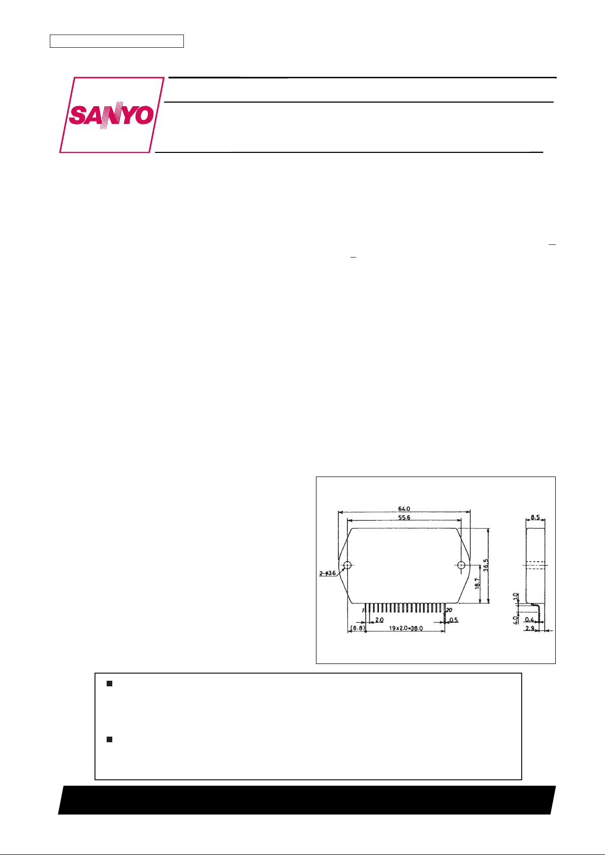
Package Dimensions
unit: mm
4150
[STK672-020]
STK672-020
SANYO Electric Co.,Ltd. Semiconductor Bussiness Headquarters
TOKYO OFFICE Tokyo Bldg., 1-10, 1 Chome, Ueno, Taito-ku, TOKYO, 110-8534 JAPAN
Unipolar Fixed-Current Chopper (separate excitation)
Type 3.0 A Output Current Stepping Motor Driver
with Built-in 4-Phase Distribution Controller
Thick-Film Hybrid IC
Any and all SANYO products described or contained herein do not have specifications that can handle
applications that require extremely high levels of reliability, such as life-support systems, aircraft’s
control systems, or other applications whose failure can be reasonably expected to result in serious
physical and/or material damage. Consult with your SANYO representative nearest you before using
any SANYO products described or contained herein in such applications.
SANYO assumes no responsibility for equipment failures that result from using products at values that
exceed, even momentarily, rated values (such as maximum ratings, operating condition ranges, or other
parameters) listed in products specifications of any and all SANYO products described or contained
herein.
Page 2
Specifications
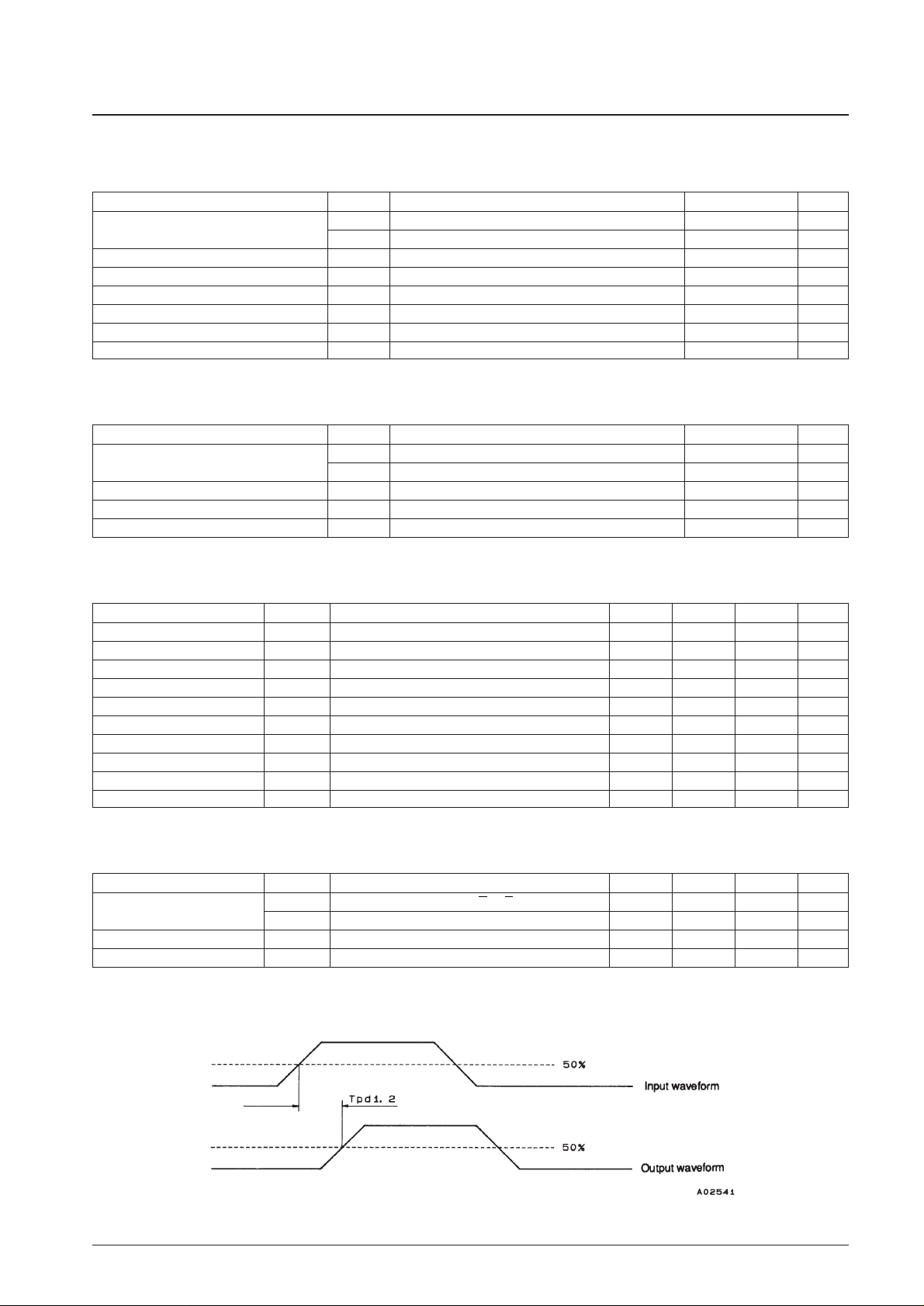
Absolute Maximum Ratings at Ta = 25°C
Allowable Operating Ranges at Ta = 25°C
Electrical Characteristics at Ta = 25°C, VCC1 = 36 V, VCC2 = 5 V
AC Characteristics at Ta = 25°C, VCC1 = 36 V, VCC2 = 5.0 V, CL= 50 pF
Note: Use a rated power supply.
Definition of the Delay Time Tpd
No. 4928-2/17
STK672-020
Parameter Symbol Conditions Ratings Unit
Maximum supply voltage
V
CC
1 max No signal 52 V
V
CC
2 max No signal 7.0 V
Maximum phase output current I
OH
max 0.5 s, 1 pulse 3.9 A
Repeat avalanche capacity Ear max 42 mJ
Input voltage V
IN
max 7.0 V
Operating substrate temperature Tc max 105 °C
Junction temperature Tj max 150 °C
Storage temperature range Tstg –40 to +125 °C
Parameter Symbol Conditions Ratings Unit
Operating supply voltage
V
CC
1 With a signal present 18 to 42 V
V
CC
2 With a signal present 5 ± 5% V
Input voltage V
IH
0 to VCC2 V
Phase drive withstand voltage V
DSS
100 V
Phase current I
OH
max Duty: 50% per phase 3.0 A
Parameter Symbol Conditions min typ max Unit
Output saturation voltage Vst R
L
= 23 Ω 1.5 2.1 V
Output current (average) Ioave Load (each phase): R = 3.5 Ω, L = 3.8 mH 0.45 0.50 0.59 A
FET diode forward voltage Vdf If = 1.0 A 1.2 1.8 V
Current when stopped Icco 36 55 mA
On input voltage V
IH
Pins 14, 15, 16, 17, 18, and 19 4.0 V
Off input voltage V
IL
Pins 14, 15, 16, 17, 18, and 19 1.0 V
Input leakage current I
I
Pins 14, 15, 16, 17, 18, and 19 –600 +30 µA
C1 to C3 high level voltage CV
OH
Pins 1, 2, and 3 2.4 V
C1 to C3 low level voltage CV
OL
Pins 1, 2, and 3 0.4 V
Chopping frequency fc R/C: 2.4 kΩ/6800 pF 35 42 50 kHz
Parameter Symbol Conditions min typ max Unit
Delay time
Tpd1 For the clock path: CLK
→ A, A, B, B 2 µs
Tpd2 For the clock path: CLK → C1, C2, C3 2 µs
Output signal interval Tin Only for 4-phase 2 excitation 20 40 µs
Maximum clock frequency f
CLK
20 kHz
Page 3
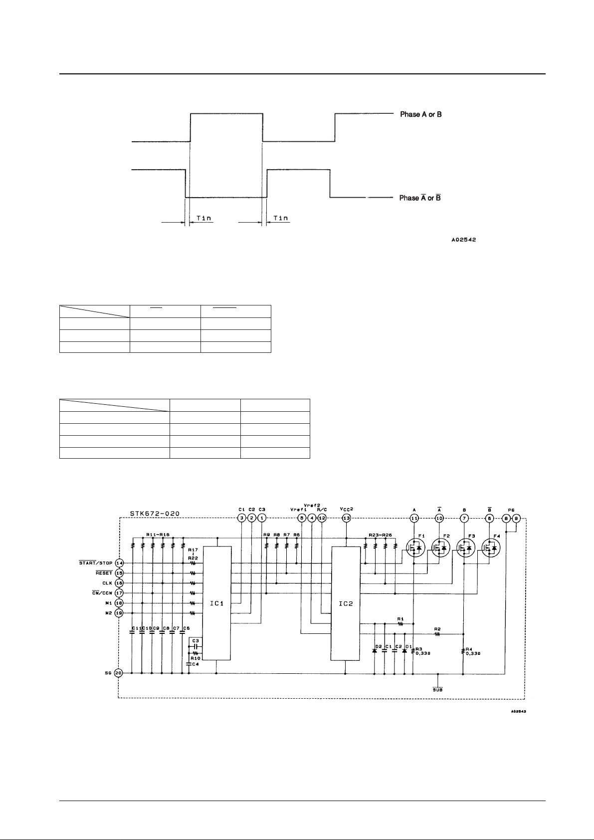
Definition of the Output Signal Interval Tin
Function Table
Operating Mode
Excitation Mode
Equivalent Circuit
No. 4928-3/17
STK672-020
CW/CCW START/STOP
CW L L
CCW H L
STOP
✕ H
M1 M2
4-phase 1 excitation L L
4-phase 2 excitation H L
4-phase 1-2 excitation L H
4-phase W1-2 excitation H H
Page 4
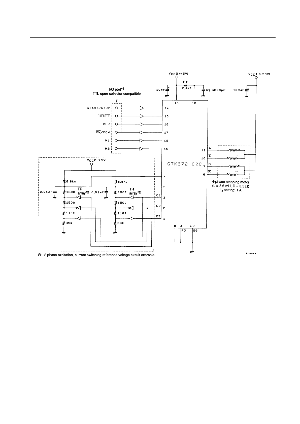
Sample Application Circuit (W1-2 phase excitation, motor current: four stage switching)
Note: 1. See the function tables and the timing chart for details on the I/O port signals.
2. Use the Sanyo LB1212, LB1214, or equivalent for the TR array.
3. The RESET pin should normally be left open.
No. 4928-4/17
STK672-020
Page 5
STK672-020 Operation
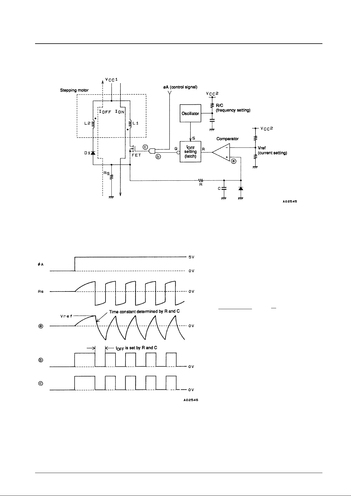
<Separate Excitation Chopper Driver Block Operation>
Fig. 1 STK672-020 Driver Block Basic Circuit
Figures 1 and 2 show the driver block basic circuit and the waveforms in the various blocks.
Unlike the earlier STK6710 Series, which adopted MOSFET transistors, the STK672-020 implements a fixed current
drive scheme with separate excitation.
Fig. 2 Waveform Timing Chart
Thus the chopping operation is partially fixed at the oscillator frequency by the latch function.
The STK672-020 repeats the operation of switching the motor current on and off, i.e., fixed current chopping operation,
as described above.
No. 4928-5/17
STK672-020
When the FET is turned on by a high level input
on the øA signal in the driver block basic circuit,
the comparator + pin goes low and the comparator
output goes low. The L1 current IONthat flows in
the FET at this time is given by the following
formula.
ION= (1 – e
– t
)..................... (1)
L: Coil inductance
R: The sum of the coil resistance and Rs
Then, when the Rs voltage becomes equal to
Vref, the FET turns off. At this point the energy
stored in the inductor L1 induces a current in L2
and the current I
OFF
flows. The time that the
current I
OFF
flows is proportional to the off time
set at the oscillator.
R
L
VCC1 – Vsat
R
Page 6
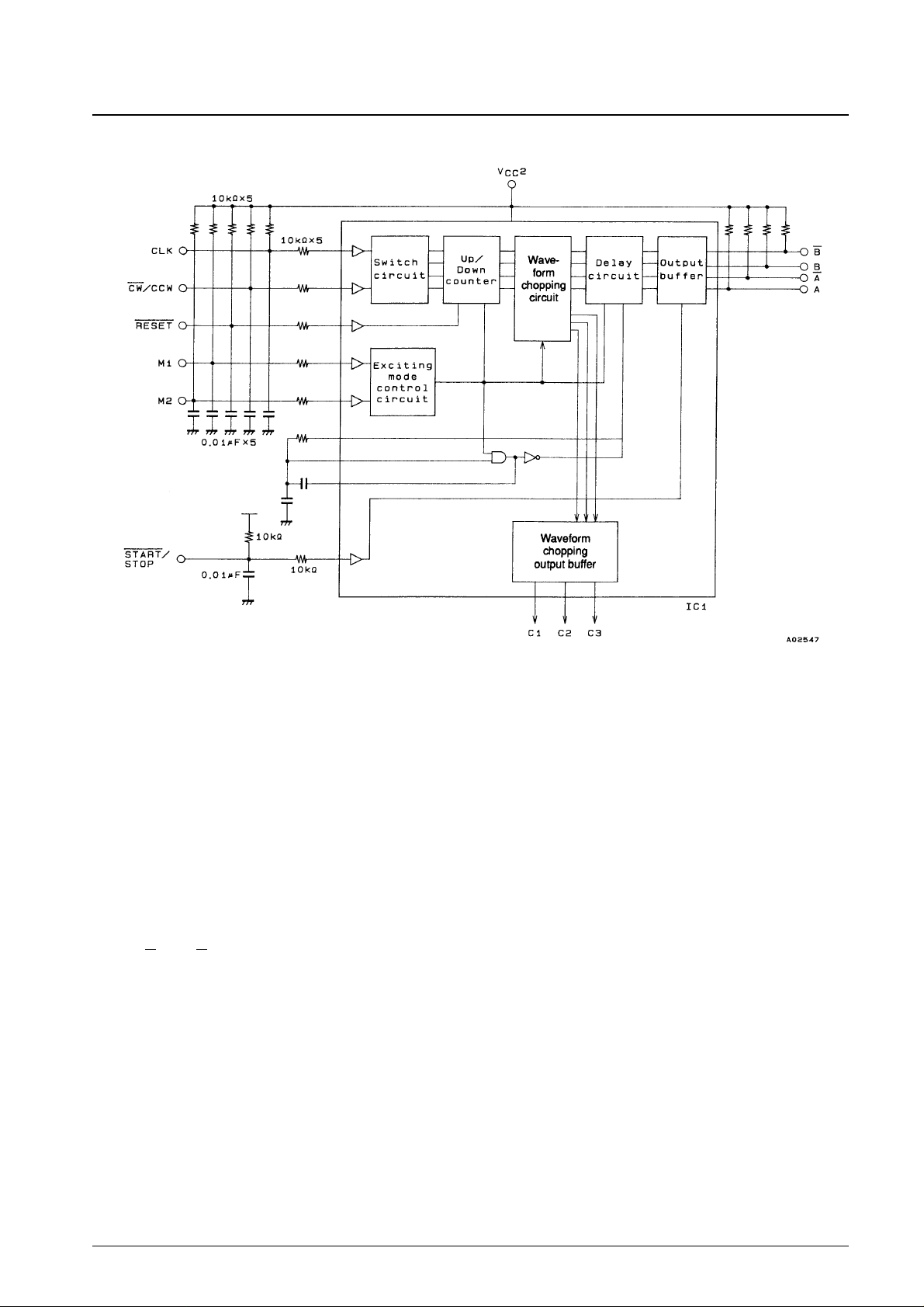
<4-Phase Distribution Control Logic Block Operation>
Fig. 3 Control Logic Circuit
The control logic IC built into the STK672-020 is a special-purpose IC developed to allow stepping motors to be
operated more simply than was possible previously.
Features
• One of four excitation types can be selected with the excitation mode setting (M1 and M2).
1. 4-phase 1 excitation
2. 4-phase 1-2 excitation
3. 4-phase 2 excitation
4. 4-phase W1-2 excitation
• Schmitt circuits are provided on all input pins (for a high noise margin).
• Inputs have 10 kΩ pull-up resistors built in so that they are CMOS and TTL input compatible. Thus the inputs can be
driven directly from I/O ports or special-purpose LSIs.
• The AA and BB phases of 4-phase control output at the 2-phase excitation set up the interval times.
• The minimum pulse width for the control logic is 25 µs. The logic operates on pulse falling edges.
The following timing charts show the logic in each excitation mode.
No. 4928-6/17
STK672-020
Page 7

Fig. 4 4-Phase 1 Excitation Timing Chart
Fig. 5 4-Phase W1-2 Excitation Timing Chart
No. 4928-7/17
STK672-020
Page 8

Fig. 6 4-Phase 2 Excitation Timing Chart
Fig. 7 4-Phase 1-2 Excitation Timing Chart
No. 4928-8/17
STK672-020
Page 9

Fig. 8 Motor Output Current Waveform
Fig. 9: Vref Peripheral Circuit
The output current range is from 0.1 A of the current caused by the t
OFF
time in oscillator to 1.7 A of the allowable
maximum current.
Notes on W1-2 Phase Excitation Current Switching
The STK672-020 provides the control logic circuit to allow the current to be switched over up to four levels by the C1,
C2, and C3. A low saturation transistor must be used on the Vref voltage switching device in the W1-2 phase excitation
circuit.
The reason for this is that when the W1-2 phase excitation current is switched over up to four levels, for switching IOat
small settings the IOwaveform will be displaced from the desired value due to variations in the VCE(sat) voltage drop of
the external Vref switching device. This can result in increased motor vibrations. Therefore we recommend selecting a
device with a VCE(sat) of about 10 mV at IC= 100 µA for this transistor at the operating conditions used for this circuit.
Note that although we proposed using the LB1212 or LB1214, this does not necessarily apply to designs that take mass
production into consideration.
The output current setting ratios for W1-2 phase excitation are 100%, 92%, 70%, and 38% for four-level switching and
100% and 70% for two-level switching. These are target values and precise adjustment should be made in the actual
circuit.
A description of the W1-2 phase excitation follows.
No. 4928-9/17
STK672-020
<Output Current Setting>
Figure 8 shows the motor output current waveform.
The output current IOHis set by the STK672-020 pin 4 (5) voltage.
The formulas for these calculations are as follows.
Vref = ×VCC2 .................................................. (2)
IOH= K × .................................................................... (3)
RS: The hybrid IC internal current detection resistor
(0.33 ± 3%)
K: 1.1 to 1.2 (correction coefficient for differences
between settings and measurements)
K is a proportionality constant that corrects for discrepancies between
measurements and settings. Since the value of K is the set value in one
condition, the value must be reset for each condition examined.
Sources of error include motor supply voltage and the motor electrical
characteristics.
Vref
R
S
RO2
RO1 + RO2
Page 10

<W1-2 Phase Excitation>
1. Overview
W1-2 phase excitation is a technique for acquiring 1/2 the step angle of the 1-2 phase excitation by controlling the
stepping motor winding currents for each phase.
2. Basic Concepts
There are three types of W1-2 phase excitation.
A: Fixed common current form
B: Square form
C: Circle form
Figure 10 shows the concepts behind these forms.
The relation between the basic step angle θOof a two (or four) phase stepping motor and W1-2 phase excitation is
given by the following formula.
θ = θO/4
In A, the common current is always a fixed value, and the motor vibration is even lower than for 1-2 phase
excitation since the motor current in each phase increases in a stepwise manner.
In B, the common currents is 2-times or 1.41-times, and although the motor current in each phase increases in a
stepwise manner, operation is rougher than type A.
In C, although the common current still increases, since the motor current in each phase increases in a stepwise
manner and the form is circular, this type is effective at reducing vibration.
3. Application
Figure 11 shows the timing chart for each block, i.e., the input clock, the each phase driver input, current control, and
the phase currents. Based on the clock, which is the rotate command for the distributor first stage, this circuit controls
the fixed current drive currents by forming each phase input as a 1-2 phase excitation sequence and forming the
current control sequence as C1, C2, and C3 in the distributor.
No. 4928-10/17
STK672-020
Page 11

A: Fixed Common Current Form
B: Square Form
C: Circle Form
Fig. 10 W1-2 Phase Excitation Control Angle Concepts
No. 4928-11/17
STK672-020
Page 12

Fig. 11 W1-2 Phase Excitation Timing Chart
No. 4928-12/17
STK672-020
Page 13

<Oscillator Frequency Setting>
The separate excitation chopping frequency f can be derived from tONand t
OFF
as follows.
tON= –CR1× In ............................................................................................................................................. (4)
t
OFF
= –C × ×In 1 – .......................................................................................... (5)
Therefore, the separate excitation chopping frequency f is given by the following formula.
f = [Hz] ............................................................................................................................................. (6)
Values of R1 = 2.4 kΩ and C = 7500 pF are appropriate to achieve the recommended time constant.
Thermal Design
The size of the heat sink required for this hybrid IC is determined by the motor output current IOH(A), the motor’s
electrical characteristics, the excitation mode, and the clock frequency fclock (Hz) of the excitation input signal. The
thermal resistance of the required heat sink can be derived from the following formula.
θc-a = [°C/W] .............................................................................................................................. (7)
Tc max = The hybrid IC case temperature (°C)
Ta = Set internal temperature (°C)
Pd = The hybrid IC average internal power dissipation (W)
The heat sink thermal resistance θc-a can be derived from the average power dissipation shown in Figure 14. Then the heat
sink area can be derived from Figure 15. Note that the ambient temperature is influenced significantly by the air circulation
conditions within the set. Therefore, the heat sink size must be determined so that back surface (the aluminum plate side) of
the hybrid IC never exceeds Tc max (105°C) under any condition in the mounted state within the end product.
Tc max – Ta
Pd
1
tON+ t
OFF
Rx
× VCC2
Rx × R
1
0.33 × VCC2
Rx × R
1
R1+ Rx
V
L
V
H
No. 4928-13/17
STK672-020
Fig. 12 R/C Waveform Fig. 13 R/C Pin Peripheral Circuit
Page 14

<Hybrid IC Internal Average Power Dissipation>
The devices with the largest power dissipations within the STK672-020 are the current control devices, the regenerated
current diodes, the current detection resistors, and the pre-drive circuits.
The power dissipations for each of the excitation modes are given by the following formulas.
1 phase excitation: Pd
1EX
= (Vst + Vdf) IOH· t2 + (Vst · t1 + Vdf · t3) ......................... (10)
2 phase excitation: Pd
2EX
= (Vst + Vdf) IOH· t2 + (Vst · t1 + Vdf · t3) ......................... (11)
1-2 phase excitation: Pd
1-2EX
= (Vst + Vdf) IOH· t2 + (Vst · t1 + Vdf · t3) ....................... (12)
W1-2 phase excitation: Pd
W1-2EX
= (Vst + Vdf) IOH· t2 + (Vst · t1 + Vdf · t3) ............ (13)
Vst: The sum of the RONand RSvoltage drops
Vdf: The sum of the FET internal diode and the RSvoltage drops
f clock: Input clock
The times t1, t2, and t3 are shown in the figure below.
t1: The time for the winding current to reach the set value
t2: The time in the fixed current chopping region
t3: The time from the point where the phase input signal is cut to the point where the regenerated reverse
power is dissipated.
Fig. 16 Motor Output Current Waveform (idealized model)
t1 ≈ × In (1 – ×IOH) ........................................................................................................ (12)
t1 ≈ × In ( ) ........................................................................................................... (13)
VCC: Motor power supply voltage (V)
L: Motor inductance (H)
R: Motor internal resistance (Ω)
IOH: Motor output current peak value (A)
The t2 and excitation frequency F values for each excitation mode are given by the following formulas.
1 phase excitation: F = f clock, t2 = – (t1 + t3) .......................................................................................... (14)
2 phase excitation: F = f clock/2, t2 = – (t1 + t3) .......................................................................................... (15)
1-2 phase excitation: F = f clock/3, t2 = – t1..................................................................................................... (16)
W1-2 phase excitation: F = f clock/7, t2 = – t1 .................................................................................................... (17)
1
F
1
F
1
F
1
F
VCC+ 0.75
IOH× R + VCC+ 0.75
–L
R
R + 0.75
V
CC
–L
R + 0.75
IOH· f clock
8
0.64 · f clock
8
IOH· f clock
4
f clock
4
IOH· f clock
2
f clock
2
IOH· f clock
2
f clock
2
STK672-020
No. 4928-14/17
Page 15

<Junction Temperature>
The junction temperature Tj for each device can be derived from the power dissipation Pds for each transistor and θj-c.
Tj = Tc + θj-c × Pds [°C]..................................................................................................................................... (18)
The average power dissipation per transistor Pds can be derived by referring to the Pd calculation formula (average
power dissipation: the total for four transistors) for each excitation mode.
Example: The power dissipation per transistor can be calculated as Pds = Pd/4.
Note that the thermal resistance of the power transistors has the following value.
θj-c for F1 to F4 = 7 °C/W
Note: When calculating the Tj for the power transistors, the power dissipation in the detection resistor is included in the
Pds value. Therefore the voltage drop for the Rs must be taken into account in the calculation.
<STK672-020 No Heat Sink Region Example>
This section presents a case where the STK672-020 can be used without a heat sink.
Conditions:
• Motor power supply voltage VCC= 42 V, stepping motor electrical characteristics: 2 mH/ø, 2 Ω/ø
• Excitation: 2 phase excitation
• Input clock: 500 Hz (fixed)
• Hybrid IC ambient temperature Ta = 25°C, natural convection
• Motor output current: 2.0 A
From these conditions and formulas (12), (13), and (15):
t1 ≈ 0.10 ms
t2 ≈ 3.81 ms
t3 ≈ 0.09 ms
The average power dissipation is calculated from formula (9) referencing Figure 17 and Figure 18.
Pd
2EX
= (Vst + Vdf) IOH· t2 + (Vst · t1 + Vdf · t3)
≈ 4.95 + 0.12 ≈ 5.07 [W]
Tc is derived from formula (7) as follows:
Tc = Pd
2EX
× θc-a + Ta = 5.07 × 14.5 + 25 ≈ 99 [°C] < Tc max = 105 [°C]
(θc-a = 14.5°C/W: the thermal resistance of the hybrid IC itself with no heat sink)
Note that the typical values of the device characteristics have been used in this example. Therefore, due also to the
details of the air flow around the hybrid IC, the actual values will not necessarily agree with this calculation, and must be
confirmed in an actual operating circuit.
IOH· f clock
2
f clock
2
No. 4928-15/17
STK672-020
Page 16

No. 4928-16/17
STK672-020
Page 17

PS No. 4928-17/17
STK672-020
This catalog provides information as of August, 1998. Specifications and information herein are subject to
change without notice.
Specifications of any and all SANYO products described or contained herein stipulate the performance,
characteristics, and functions of the described products in the independent state, and are not guarantees
of the performance, characteristics, and functions of the described products as mounted in the customer’s
products or equipment. To verify symptoms and states that cannot be evaluated in an independent device,
the customer should always evaluate and test devices mounted in the customer’s products or equipment.
SANYO Electric Co., Ltd. strives to supply high-quality high-reliability products. However, any and all
semiconductor products fail with some probability. It is possible that these probabilistic failures could
give rise to accidents or events that could endanger human lives, that could give rise to smoke or fire,
or that could cause damage to other property. When designing equipment, adopt safety measures so
that these kinds of accidents or events cannot occur. Such measures include but are not limited to protective
circuits and error prevention circuits for safe design, redundant design, and structural design.
In the event that any and all SANYO products described or contained herein fall under strategic
products (including services) controlled under the Foreign Exchange and Foreign Trade Control Law of
Japan, such products must not be exported without obtaining export license from the Ministry of
International Trade and Industry in accordance with the above law.
No part of this publication may be reproduced or transmitted in any form or by any means, electronic or
mechanical, including photocopying and recording, or any information storage or retrieval system,
or otherwise, without the prior written permission of SANYO Electric Co., Ltd.
Any and all information described or contained herein are subject to change without notice due to
product/technology improvement, etc. When designing equipment, refer to the “Delivery Specification”
for the SANYO product that you intend to use.
Information (including circuit diagrams and circuit parameters) herein is for example only; it is not
guaranteed for volume production. SANYO believes information herein is accurate and reliable, but
no guarantees are made or implied regarding its use or any infringements of intellectual property rights
or other rights of third parties.
 Loading...