SANYO STK672, STK672-040 Datasheet

Ordering number: EN 5227A
Thick Film Hybrid IC
STK672-040
Microstep Operation-Supported
4-Phase Stepping Motor Driver (I
= 1.5A)
O
Overview
The STK672-040 is a unipolar constant-current choppertype externally-excited 4-phase stepping motor driver
hybrid IC which uses MOSFET power devices. It has a
microstep operation-supported 4-phase distributed controller built-in to realize a high torque, low vibration, low
noise stepping motor driver using a simple control circuit.
Applications
• Printer, copier, and X-Y plotter stepping motor drivers
Features
• Microstep sine-wave driver operation using only an
external clock input (0.33 Ω current detection resistor
built-in)
• Microstep drive using only an external reference v oltage
setting resistor
• 2, 1-2, W1-2, 2W1-2, 4W1-2 phase excitation selectable
using external pins
• Selectable vector locus (perfect circle mode, inside 1
mode, outside 2 modes) to match motor characteristics
in microstep drive state
• Phase hold function during excitation switching
• Schmitt trigger inputs with built-in pull-up resistor
(20k Ω )
• Monitor output pin enabling real-time confirmation of
IC excitation
• The CLK and RETURN inputs provide an internal
noise elimination circuit as well as CMOS Schmitt circuit to prevent malfunction due to impulse noise.
• 4-phase distribution switch timing selected externally to
either CLK rising-edge only detection mode or both rising-edge and falling-edge detection mode
• ENABLE pin for excitation current cutoff, thereby
reducing system current drain when driver is stopped
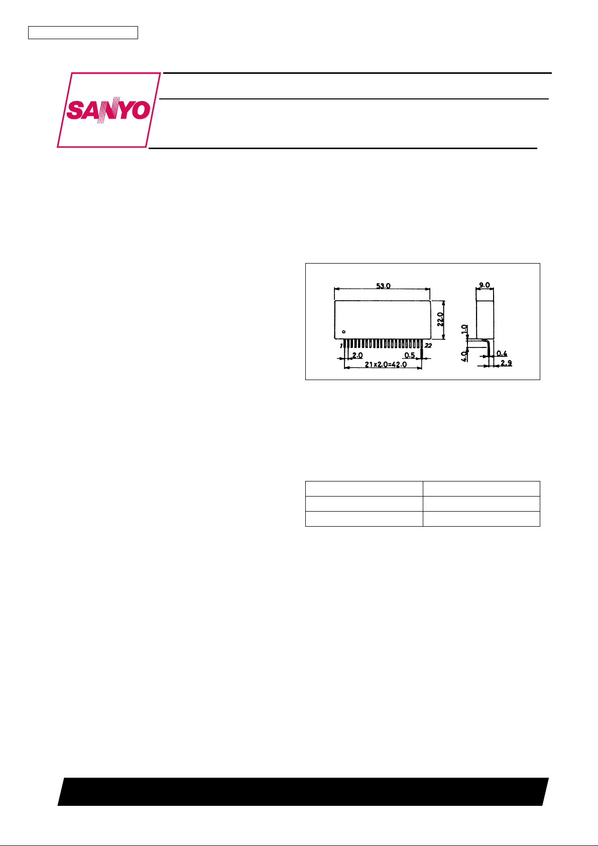
Package Dimensions
unit: mm
4161
[STK672-040]
Series Organization
The following devices form a series with differing output
capacity.
Type No. Output current (A)
STK672-040 1.5
STK672-050 3.0
SANYO Electric Co., Ltd. Semiconductor Business Headquarters
TOKYO OFFICE Tokyo Bldg., 1-10, 1 Chome, Ueno, Taito-ku, TOKYO, 110 JAPAN
10997HA(ID) / 110896HA(ID) No. 5227—1/11

Specifications
−
−
°
°
−
° C
Ω
µ
µ A
µ A
STK672-040
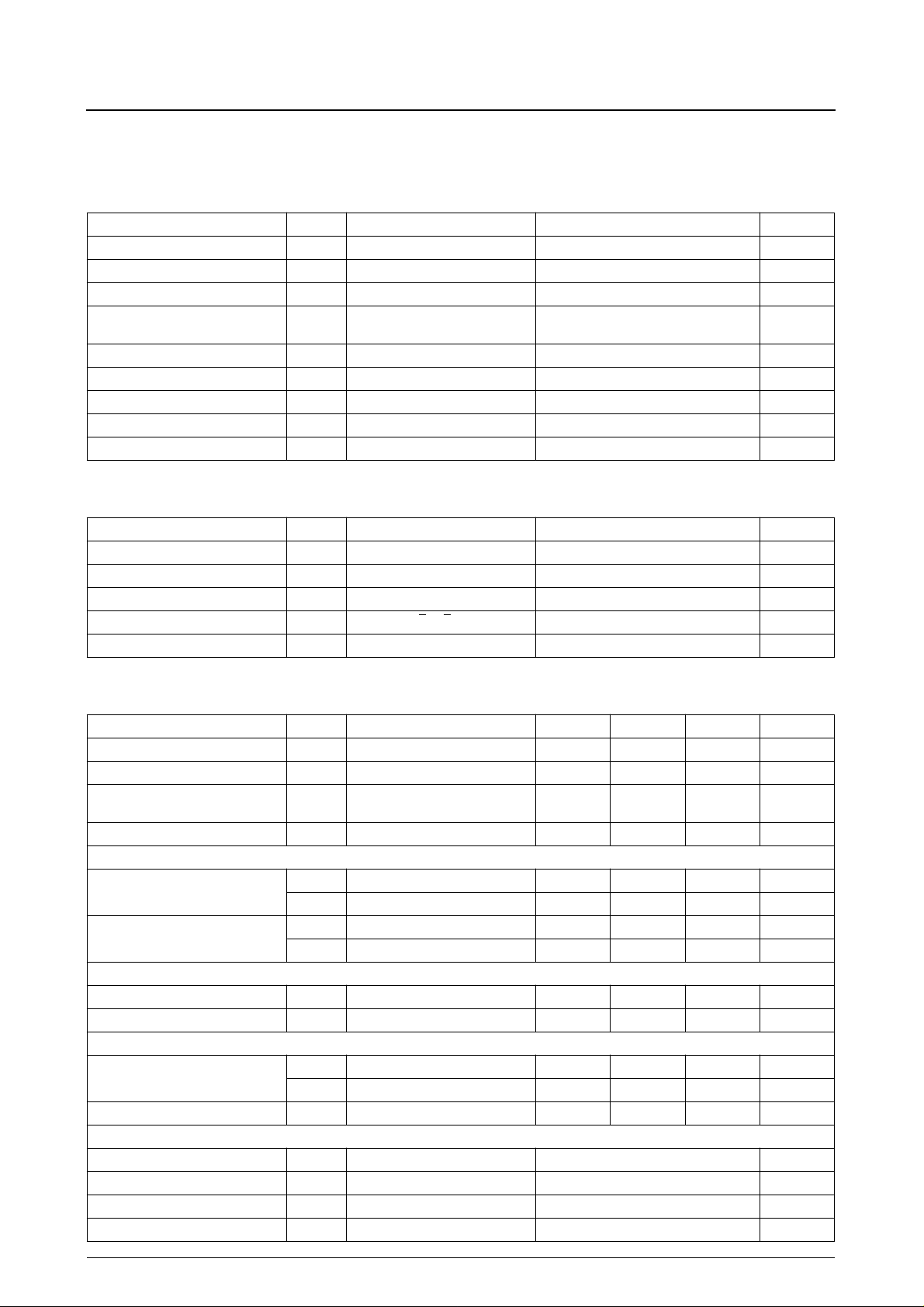
Maximum Ratings
at Ta = 25 ° C
Parameter Symbol Conditions Ratings Unit
Maximum supply voltage 1
Maximum supply voltage 2 V
Input voltage V
Phase output current I
V
1 max No signal 52 V
CC
2 max No signal
CC
max Logic input block
IN
One 0.5s pulse, V
max
OH
Load/phase: R = 5 Ω , L = 10mH
1 applied,
CC
0.3 to +7.0 V
0.3 to +7.0 V
2.2 A
Repetitive avalanche handling capability Ear max 38 mJ
Maximum output dissipation Pd max θ c–a = 0 12 W
Operating substrate temperature Tc max 105
Junction temperature Tj max 150
Storage temperature Tstg
Allowable Operating Ranges
at Ta = 25 ° C
40 to +125
Parameter Symbol Conditions Ratings Unit
Supply voltage 1 V
Supply voltage 2 V
Input voltage V
Phase driver withstand voltage V
Phase current I
1 With signal 10 to 45 V
CC
2 With signal 5.0 ± 5% V
CC
0 to V
IH
Tr1, 2, 3, 4 (A, A
DSS
max 50% duty 1.5 (max) A
OH
, B, B outputs) 100 (min) V
2V
CC
C
C
Electrical Characteristics
at Tc = 25 ° C, V
1 = 24V, V
CC
CC
2 = 5V
Parameter Symbol Conditions min typ max Unit
Control supply current I
Output saturation voltage Vsat R
Average output current Io ave
Pin 7 input, ENABLE = low – 4.5 15 mA
CC
= 15 Ω (I = 1.5A) – 1.4 1.9 V
L
Vref = 1V,
Load/phase: R = 3.5
, L = 3.8mH
0.465 0.517 0.569 A
FET diode forward voltage Vdf If = 1.0A – 1.2 1.8 V
[Control inputs]
V
Excluding Vref pin 4.0 – – V
Input voltage
Input current
IH
V
Excluding Vref pin – – 1.0 V
IL
I
Excluding Vref pin 0 1 10
IH
I
Excluding Vref pin 125 250 510
IL
[Vref input]
Input voltage V
Input current I
Pin 8 0 – 2.5 V
I
Pin 8 – 1 –
I
[Control outputs]
V
I = − 3mA (MoI, Mo1, Mo2 pins) 2.4 – – V
Output voltage
OH
V
I = +3mA (MoI, Mo1, Mo2 pins) – – 0.4 V
OL
PWM frequency fc 37 47 57 kHz
[Current division ratio (A/B)]
2W1-2, W1-2, 1-2 Vref θ = 1/8 100 %
2W1-2, W1-2 Vref θ = 2/8 92 %
2W1-2 Vref θ = 3/8 83 %
2W1-2, W1-2, 1-2 Vref θ = 4/8 71 %
A
No. 5227—2/11

STK672-040
2W1-2 Vref θ = 5/8 55 %
2W1-2, W1-2 Vref θ = 6/8 40 %
2W1-2 Vref θ = 7/8 20 %
2 Vref 100 %
Note: All tests are made using a constant-voltage supply.
The current division ratio shows the design value.
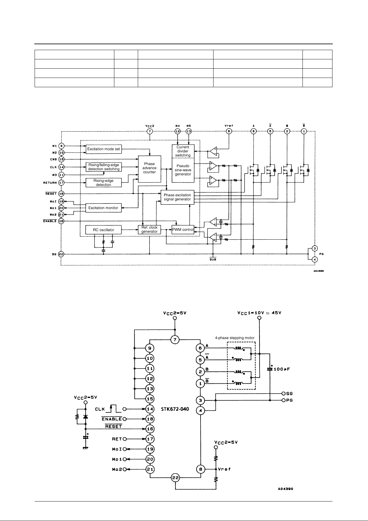
Equivalent Block Diagram
Sample Application Circuit
2W1-2 phase excitation (microstep operation)
No. 5227—3/11

STK672-040
Motor Current Calculation
The motor current I
age on pin 8 (Vref). The relationship between I
Vref is given by the following equation.
1
OH
---
Vref Rs ⁄×
=
3
I
is determined by the reference volt-
OH
OH
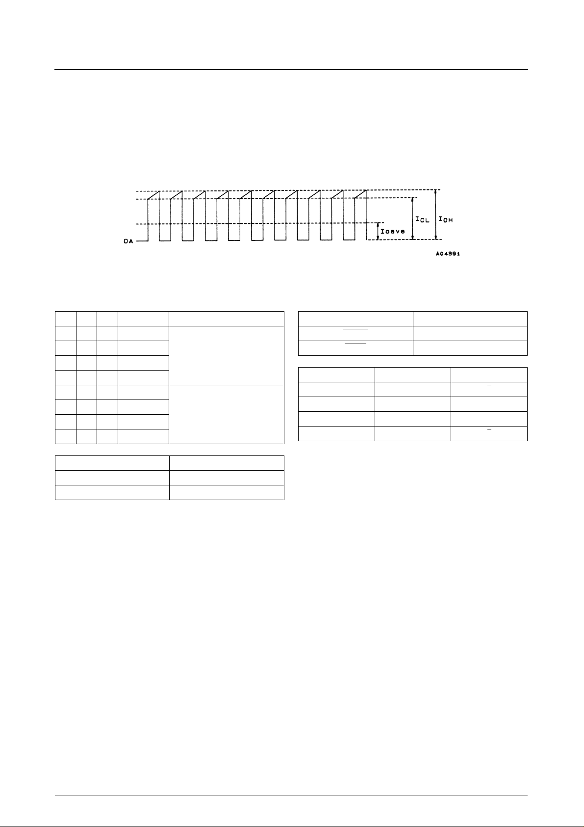
Motor current waveform
Function T ables
M1 M2 M3 Excitation Phase switching CLK edge timing
0 0 0 Phase 1-2
0 1 0 Phase 2W1-2
1 0 0 Phase W1-2
1 1 0 Phase 4W1-2
0 0 1 Phase 2
0 1 1 Phase W1-2
1 0 1 Phase 1-2
1 1 1 Phase 2W1-2
Rising and falling edge
Rising edge only
and
where Rs is the built-in current detection resistance
(0.33 Ω ± 3%).
The motor current ranges from the current due to the frequency duty set by the oscillator (0.05 to 0.1A) to the
allowable operating range maximum of I
Input Active level
ENABLE
RESET Low
Mo1 Mo2 Output
00A
01B
10A
11B
= 1.5A.
OH
Low
CWB Direction
0 Forward
1 Reverse
No. 5227—4/11
 Loading...