

Page 1
Ordering number : EN 4873
N2894TH (OT) No. 4873-1/12
Overview
The STK6217 is a hybrid IC that combines in a single
package a unidirectional DC motor driver, a PLL
constant-speed controller (the LC7991) and associated
peripheral components, including a separately excited
oscillator, a comparator, and an FG amplifier. The motor
controller uses a PLL circuit for precise motor control.
The wide range of the STK6217’s FG lock frequency
allows it to handle a wide range of applications. Since the
motor driver block uses MOSFET devices as power
elements, it features high output currents (rush current)
and low loss.
Applications
• Plain paper copier DC motor drivers
• FAX paper transport motor drivers
• Other DC motor applications
Features
<Motor Controller Block>
• High FG frequency upper limit (locking range: 200 to
2500 Hz)
• Built-in FG divider (FG lock upper limit with divider in
use: 5000 Hz)
• Speed lock indicator output directly drives an external
LED.
• TTL level compatible ROT input
<Motor Driver Block>
• MOSFET power elements provide high output currents
(rush current).
• Low-loss PWM speed controller (built-in externally
excited oscillator: 25 kHz)
• Wide power supply voltage range (V
DSS
= 60 V)
• Built-in motor start-up overcurrent limiter function
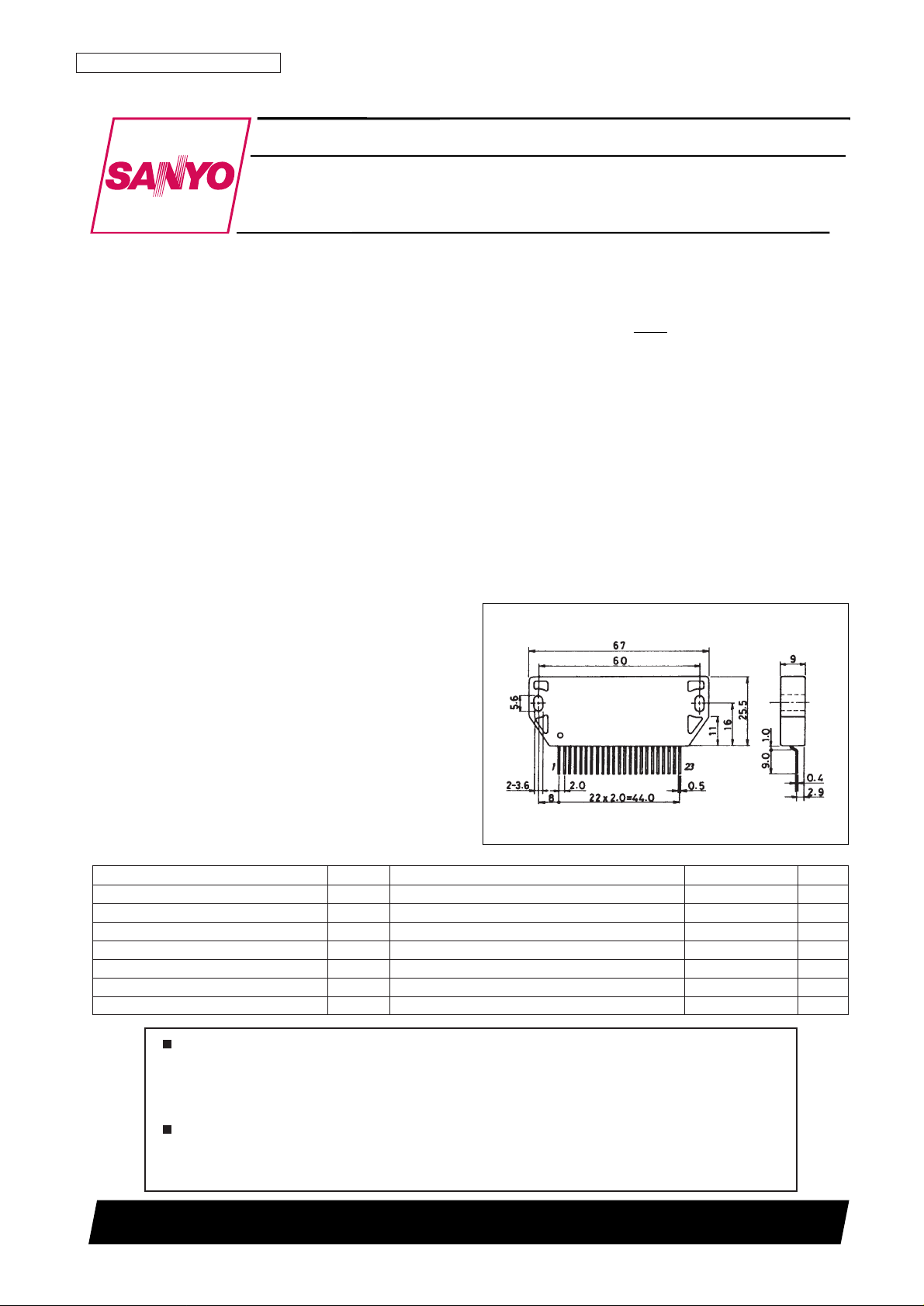
Package Dimensions
unit: mm
4138
STK6217
SANYO Electric Co.,Ltd. Semiconductor Bussiness Headquarters
TOKYO OFFICE Tokyo Bldg., 1-10, 1 Chome, Ueno, Taito-ku, TOKYO, 110-8534 JAPAN
Unidirectional DC Motor Driver with Constant-Speed
Digital Servo Controller (output current: 8 A)
Thick Film Hybrid IC
Any and all SANYO products described or contained herein do not have specifications that can handle
applications that require extremely high levels of reliability, such as life-support systems, aircraft’s
control systems, or other applications whose failure can be reasonably expected to result in serious
physical and/or material damage. Consult with your SANYO representative nearest you before using
any SANYO products described or contained herein in such applications.
SANYO assumes no responsibility for equipment failures that result from using products at values that
exceed, even momentarily, rated values (such as maximum ratings, operating condition ranges, or other
parameters) listed in products specifications of any and all SANYO products described or contained
herein.
Specifications
Absolute Maximum Ratings at Ta = 25°C
Parameter Symbol Conditions Ratings Unit
Maximum supply voltage 1 V
CC
1 max No signal 52 V
Maximum supply voltage 2 V
CC
2 max No signal 7 V
Maximum motor rush current I
O
peak max Duty 1%, period ≤ 100 ms 18 A
Maximum input voltage V
IH
max 7V
Storage temperature range Tstg –40 to +125 °C
Junction temperature Tj max 150 °C
Operating substrate temperature Tc max 105 °C
[STK6217]
Page 2
Allowable Operating Ranges at Ta = 25°C
Operating Characteristics at Ta = 25°C, V
CC
1 = 24 V, VCC2 = 5.0 V
Pin Functions
No. 4873-2/12
STK6217
Ratings
Parameter Symbol Conditions
min typ max
Unit
V
CC
2 current dissipation I
CC
When the ROT input is used 10 15 mA
Output FET saturation voltage V
SAT
RL= 3 Ω 0.95 1.3 V
Built-in oscillator frequency f
O
21 25 31 kHz
OSC output amplitude V
OP-P
1.9 2.3 2.7 Vp-p
OSC output effective amplitude Vorms Pin 7 output voltage 0.54 0.66 0.80 Vrms
Common mode input voltage range V
ICM
Integrating amplifier and FG amplifier
0 V
CC
2 – 1.5 V
input voltage
FG amplifier feedback resistance R
f
95 100 105 kΩ
High input level voltage V
IH
DIV1 to DIV3, PR1, PR2 and ROT
0.7 V
CC
2 VCC2 V
inputs
Low input level voltage V
IL
0 0.3 VCC2 V
High input level current I
IH
DIV1 to DIV3, PR1 and PR2 inputs 1 µA
Low input level current I
IL
–1 µA
High output level current I
OH
Lock input VOH= VCC2 – 0.4 V –2 mA
Low output level current I
OL
Lock input VOL= 0.4 V 2 mA
Input frequency range
f
XI
XI input 0.1 10.5 MHz
f
FG
FGI input 50 kHz
FG lock frequency
f
FLOCK
FG input divider off 200 2500 Hz
f
FLOCK
FG input divider on 400 5000 Hz
Output cut voltage Vocut Pin 5 input voltage 0 25 mV
Pin No. Symbol Function
1
OUT Motor output
2
3
Vrs Current detection resistor connection
4
5 Vref4 Motor start-up current control reference voltage
6 V
CC
2 Power supply voltage input (+5 V)
7 Vref1 H/IC built-in oscillator bias voltage setting
8 Vref2 Integrating amplifier reference voltage setting
9 Vref3 FG input reference voltage setting
10 FG FG input
11 R
f
Integrating amplifier output
12 Mix in Integrating amplifier input
13 Mix out PO and FO sum output (PO and FO each have a 100 kΩ output resistance.)
14 XI Crystal oscillator connection (input)
15 XO Crystal oscillator connection (output)
16 DIV1
17 DIV2 Variable divider setting
18 DIV3
19 PR1
Phase comparison range select
20 PR2
21 ROT Motor rotate/stop input; H: stop, L: rotate
22 Lock Lock output; Outputs a low level when locked
23 SG Ground
Parameter Symbol Conditions Ratings Unit
Operating supply voltage 1 V
CC
1 Input active 10 to 42 V
Operating supply voltage 2 V
CC
2 Input active 5 ± 5% V
Motor output current I
O
DC (Tc = 25°C) 8 A
FET withstand voltage V
DSS
60 min V
Input voltage V
IH
VCC2 V
Page 3
I/O Formats
Pin No. Format
No. 4873-3/12
STK6217
16, 17, 18, 19
14, 15
21
22
13
Page 4
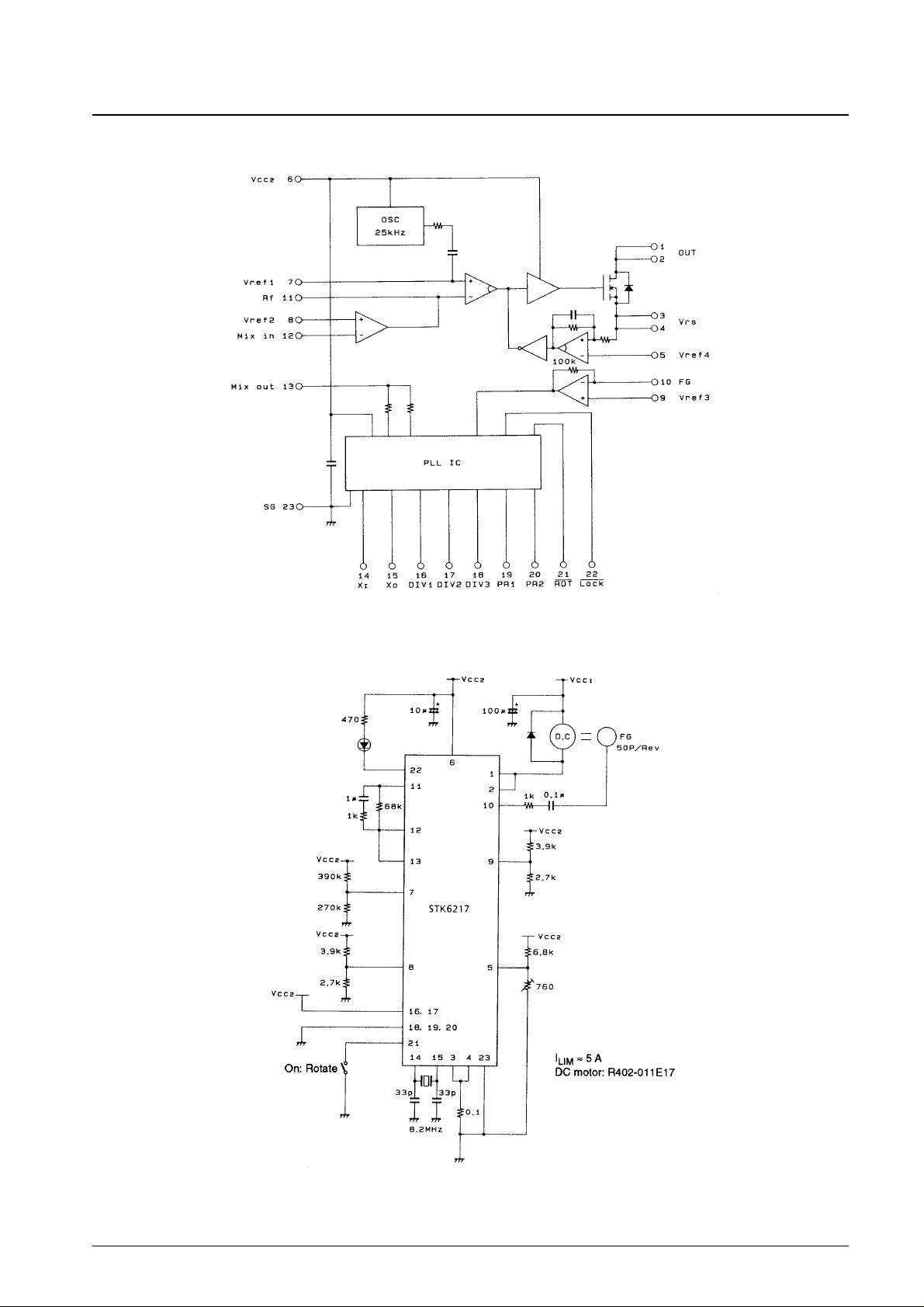
Equivalent Circuit
Sample Application Circuit
No. 4873-4/12
STK6217
The circuit shown above locks at an FG frequency of 2000 Hz.
Reference frequency: 8.2 MHz
Variable divider: 1/2
FG divider: Off
Unit (resistance: Ω, capacitance: F)
Unit (resistance: Ω, capacitance: F)
Page 5

Operating Principles
1. Overview
Figure 1 shows the block diagram for the STK6217. The PLL control block compares the frequencies and phases of the
FG signal frequency fed back from the motor with a reference clock, which is formed by dividing a reference signal.
When they agree, the frequency is locked with a 50% duty. The control signals consist of two systems with D/A
converted outputs: FO, which is the frequency control output and PO, which is the phase control output. Since PLL
control provides a motor speed that is synchronized with a reference clock frequency fref, which is created by dividing a
reference signal, the stability of fref directly influences the stability of the rotation. Therefore, quartz precision digital
control is possible by using a crystal oscillator for reference signal generation. The control signals are added by an
integration circuit, which also functions as an active filter. It is here that the servo system gain and phase compensation
are performed. The output of this system is sent to the PWM conversion block and a PWM signal, which is based on the
period of an associated oscillator circuit, is input to the unidirectional driver of the final stage, which drives the DC
motor.
2. Motor Speed, Resonant Frequency, and Encoder Pulse Count
The frequency fFGof the signal generated by the encoder is given by:
fFG(Hz) =
N (rpm)
× P (P/R).........................................................................................
①
60
Where, N: Motor speed (rpm)
P: Number of pulses per encoder rotation
Formula ①can be transformed as follows:
N (rpm) =
60 × f
FG
........................................................................................................
②
P (P/R)
Alternatively,
P (P/R) =
60 × f
FG
........................................................................................................
③
N
Here, the relationship with the oscillator resonant frequency is given by:
N (rpm) =
60
×
fxtal
..........................................................................
④
P DIV × 2050 (1025)
Alternatively,
P (P/R) =
60
×
fxtal
..........................................................................
⑤
N DIV × 2050 (1025)
Here, DIV: Variable divider ratio
See item 3-1, subsection (3).
The value (1025) is used when the fFGinput frequency is divided by 2 (as determined by DIV setting).
See item 3-1, subsection (3).
Note that the following three methods for increasing the stability of the motor speed can be considered.
①
Increasing the number of encoder output pulses for a given motor speed.
②
Not using the FG divider if at all possible, since using it decreases the precision of the rotation data.
③
Setting the divider ratio to as low a value as possible, so that the oscillator precision is not reduced.
No. 4873-5/12
STK6217
Page 6

Figure 1 STK6217 Block Diagram
Figure 2 PLL IC Block Diagram
No. 4873-6/12
STK6217
Page 7

3. Block Functional Descriptions
3-1 Reference Signal Generation Block
(1) Crystal oscillator circuit
The controller block generates a reference clock using a crystal oscillator and a capacitor connected to the XI and
XO pins. It is also possible to leave the XO pin open and input an external clock to the XI pin.
(2) Crystal resonant frequency calculation
After determining the FG frequency to be locked, use the following formula to derive the required crystal frequency.
a) With the FG divider off
fxtal = f
FGLock
× DIV × 2050 (Hz)
b) With the FG divider on
fxtal = f
FGLock
× DIV × 1025 (Hz)
Where:
fxtal: Crystal resonant frequency
f
FGLock
: The FG frequency to be locked
DIV: The variable divider ratio
(3) Variable divider and the FG divider
The controller block includes a 6-setting variable divider and an FG divider (divide-by-2, by-passable) to expand the
range of input FG frequencies. These dividers are controlled by the three pins DIV1, DIV2 and DIV3 as shown in
Table 1.
Table 1 Divider Control
No. 4873-7/12
STK6217
Control input
Variable divider ratio FG divider
DIV3 DIV2 DIV1
High level High level High level 20 OFF
High level High level Low level 10 OFF
High level Low level High level 6 OFF
High level Low level Low level 3 OFF
Low level High level High level 2 OFF
Low level High level Low level 1 OFF
Low level Low level High level 2 ON
Low level Low level Low level 1 ON
External clock inputReference oscillator calculation
The external clock
should be a square
wave with an
amplitude of 5 V
and a duty of
approximately 50%.
V
DD
= 5 V.
Page 8

3-2 Servo Control Block
The servo block compares the reference clock generated by the reference signal generation block with the FGI input (the
FG signal input from the motor) and generates three output signals: FO (frequency system control output), PO (phase
system control output), and Lock (the lock indicator output). The FO and PO outputs are 8-bit D/A converter outputs.
The motor drive signal is created from these two outputs. The Lock output indicates whether the motor is within the lock
range.
(1) Servo Operation
Control system operation is divided into the following three aspects depending on the input FG frequency: drive,
tracking (locked), and brake.
FG input frequency Operation Lock output FO output PO output
> f
FGLock
+6% Brake High level Low level Low level
Overspeed
f
FGLock
±6% Tracking Low level DA output (frequency- DA output (phase-
Lock range voltage conversion) voltage conversion)
> f
FGLock
–6% Drive High level High level High level
Underspeed
Notes
f
FGLock
=
fxtal
(Hz) Caution: The value in parentheses is used when the FG divider is on.
DIV × 2050 (1025)
f
FGLock
: FG frequency when locked; fxtal: Crystal resonant frequency; DIV: Variable divider ratio
• The drive operation is performed at start-up (underspeed) time.
• When the FO and PO outputs are set to the high level, the motor is driven at full speed.
• Braking operation is performed when the motor is in overspeed range.
• When the FO and PO outputs are set to the low level, the motor brake is applied.
• The servo control block controls the motor by using these two operations to pull the motor speed into the lock range.
(Note that the operations described up to this point are the rough adjustments performed by the frequency system.)
(2) FO and PO outputs (frequency system control output and phase system control output)
When the FG input frequency enters the lock range, the servo control switches to tracking operation. Frequency system
fine control and phase system control starts, and the FO and PO outputs are switched to voltage outputs from internal
D/A converters. Since the internal D/A converters are 8-bit converters, these output voltages have 256 possible levels.
The figures below show the FO and PO output characteristics.
●FO Output Characteristics
●PO Output Characteristics (during tracking)
No. 4873-8/12
STK6217
Caution: These characteristics are for units in the standard comparison range.
Page 9

3-3 Accessory Functions
(1) ROT input (rotate/stop)
The ROT input turns the motor on or off.
ROT input State FO output PO output
High level Stop Low level Low level
Low level Operate
* *
*
: Determined by the motor control function.
(2) PRS1 and PRS2 inputs (phase comparison range selection)
The phase system comparison range can be switched using the PRS1 and PRS2 inputs.
Phase System Comparison Range Selection
PRS2 input PRS1 input Range name Comparison range Phase output frequency
Low level Low level Standard range 2 π Once every FG input
Low level High level Test mode ········· ·····················
High level Low level Double range 6 π Once every two FG inputs
High level High level Quadruple range 14 π Once every four FG inputs
Caution: The phase range becomes more than two and four times the normal range due to the operation of a built-
in limiter. These phase output frequency values are divided by two when the FG divider is used.
●Phase Output Characteristics
Caution: The “phase difference” is the phase difference in the FG signal input with respect to the internal reference signal. The double and quadruple ranges
have hysteresis.
●FG Clock Frequencies (examples)
Oscillator resonant frequency (MHz)
Variable divider ratio FG divider
2.05 4.1 6.15 8.2 10.25
Unit
20 50 100 150 200 250 Hz
10 100 200 300 400 500 Hz
6 OFF 116 333 500 667 833 Hz
3 333 667 1000 1333 1667 Hz
2
500 1000 1500 2000 2500 Hz
ON 1000 2000 3000 4000 5000 Hz
The following two ceramic oscillators, which are available as commercial products, can be used.
CSA6.14MT (Murata) ... Handles FG frequencies of 500, 1000 and 1500 Hz.
CSA8.20MT (Murata) ... Handles an FG frequency of 2000 Hz.
No. 4873-9/12
STK6217
Page 10

4. Rush Current Limiter Circuit
4-1 Circuit Purpose
The STK6217 provides a function that can limit the current when the motor starts (or brakes). This function allows
the external current (peak) output capacity to be reduced. The rush current limit value can be changed arbitrarily by
adjusting the value of an external resistor.
4-2 Setting the Limit Value
Figure 3 shows the method for setting the limit value. The Vref voltage is adjusted by changing the value of RO2.
Formula 6 is the formula for the limit value, I
LIM
.
RO1: 6.8 kΩ (fixed)
RO2: Variable
VCC2: 5 V
Rs: Current detection resistance (Ω)
Figure 3 External Peripheral Circuit and Motor Start-up Timing Chart
Caution: • Here, the Vref voltage must be set in a range that fulfills the following condition.
Vref ≥ 0.025 V (However, VCC2 = 5 V ±5% is the alteration condition.)
The limiter function will not operate if the above condition is not met.
• Although formula ⑥can be used as a rough formula for setting the output current, the actual value will
differ due to the influence of voltage drops due to the ground pattern design external to the hybrid IC.
Therefore we recommend that I
LIM
final confirmation be performed in a circuit that has a form close to that
of the PCB final pattern.
4-3 Value of the Current Detection Resistor (Rs)
Rs detects current flowing from the motor, and the voltage drop across Rs is sensed by an internal comparator.
When an external Rs is connected to the STK6217, a resistor with a value that fulfills the following condition must
be used.
Rs × I
LIM
≤ 0.5 V ...........................................................................................................
⑦
Also, the PCB pattern should be designed so that Rs, RO2 and the STK6217’s ground pin (pin 23) are connected to
a single ground point as close as possible to the STK6217 in the pattern. In particular, Rs and the STK6217’s pins 3
and 4 must not be located any significant distance from the IC.
No. 4873-10/12
STK6217
I
LIM
(A) ≈
RO2
× VCC2 ×
1
............................................................................
⑥
RO1 + RO2 Rs
↓
Vref
Page 11

5. MOSFET Drain-Source Overvoltage
When using the STK6217, a diode is connected in parallel with the DC motor as a regenerative diode for the motor. This
also functions as a protective measure against excessive MOSFET flyback voltage. Flyback voltage is due to the
influence of circuit factors such as lead inductances, and will remain when the MOSFET turns off. (In general, these
voltages are a few volts for periods of up to 0.5 µs.) Therefore, as a final circuit operation check, confirm that the flyback
voltage does not exceed V
OSS
.
6. Thermal Design
Applications must be designed so that the temperature of the STK6217’s aluminum substrate side never exceeds 105°C
in any situation. The remainder of this section discusses thermal design for the STK6217.
6-1 Hybrid IC Average Internal Loss Derivation
The main component of the average internal loss occurs in the MOSFET, which is the PWM element.
The MOSFET loss is expressed as follows:
Pd (W) = V
SAT
× IM× fp × tON..........................................................................................
⑧
V
SAT
: FET saturation voltage
IM: Motor output peak current
tO: FET on time
fp: IC internal oscillator frequency
6-2 Deriving the heat sink size
Formula ⑨shows the thermal resistance of the required heat sink.
θc-a (°C/W) =
Tc max – Ta
............................................................................................
⑨
Pd
A heat sink that is appropriate for θc-a must be selected. (Note that θc-a for the STK6217 is 18.5°C/W.)
No. 4873-11/12
STK6217
Page 12

PS No. 4873-12/12
STK6217
This catalog provides information as of August, 1998. Specifications and information herein are subject to
change without notice.
Specifications of any and all SANYO products described or contained herein stipulate the performance,
characteristics, and functions of the described products in the independent state, and are not guarantees
of the performance, characteristics, and functions of the described products as mounted in the customer’s
products or equipment. To verify symptoms and states that cannot be evaluated in an independent device,
the customer should always evaluate and test devices mounted in the customer’s products or equipment.
SANYO Electric Co., Ltd. strives to supply high-quality high-reliability products. However, any and all
semiconductor products fail with some probability. It is possible that these probabilistic failures could
give rise to accidents or events that could endanger human lives, that could give rise to smoke or fire,
or that could cause damage to other property. When designing equipment, adopt safety measures so
that these kinds of accidents or events cannot occur. Such measures include but are not limited to protective
circuits and error prevention circuits for safe design, redundant design, and structural design.
In the event that any and all SANYO products described or contained herein fall under strategic
products (including services) controlled under the Foreign Exchange and Foreign Trade Control Law of
Japan, such products must not be exported without obtaining export license from the Ministry of
International Trade and Industry in accordance with the above law.
No part of this publication may be reproduced or transmitted in any form or by any means, electronic or
mechanical, including photocopying and recording, or any information storage or retrieval system,
or otherwise, without the prior written permission of SANYO Electric Co., Ltd.
Any and all information described or contained herein are subject to change without notice due to
product/technology improvement, etc. When designing equipment, refer to the “Delivery Specification”
for the SANYO product that you intend to use.
Information (including circuit diagrams and circuit parameters) herein is for example only; it is not
guaranteed for volume production. SANYO believes information herein is accurate and reliable, but
no guarantees are made or implied regarding its use or any infringements of intellectual property rights
or other rights of third parties.
 Loading...