

Page 1
Any and all SANYO products described or contained herein do not have specifications that can handle
applications that require extremely high levels of reliability, such as life-support systems, aircraft’s
control systems, or other applications whose failure can be reasonably expected to result in serious
physical and/or material damage. Consult with your SANYO representative nearest you before using
any SANYO products described or contained herein in such applications.
SANYO assumes no responsibility for equipment failures that result from using products at values that
exceed, even momentarily, rated values (such as maximum ratings, operating condition ranges,or other
parameters) listed in products specifications of any and all SANYO products described or contained
herein.
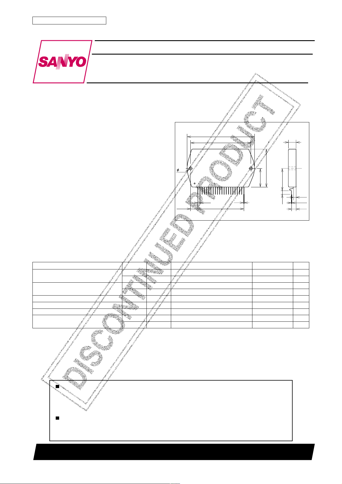
Thick Film Hybrid IC
3ch AF Power Amplifier (Split Power Supply)
(25W + 50W + 25W, THD = 0.4%)
Ordering number:ENN5247
STK400-490
SANYO Electric Co.,Ltd. Semiconductor Company
TOKYO OFFICE Tokyo Bldg., 1-10, 1 Chome, Ueno, Taito-ku, TOKYO, 110-8534 JAPAN
Overview
The STK400-490 is an audio power amplifier IC for multichannel speaker applications. It comprises two 25W channels (left and right) and a 50W channel (center) in a single
package. It is fully pin compatible with the 3-channel output devices (STK400-×00 series) and 2-channel output devices (STK401-×00 series). In addition, it supports 6/3Ω
output load impedance.
Features
• Pin compatible with the 3-channel output devices
(STK400-×00 series) and 2-channel output devices
(STK401-×00 series)
• Output load impedance R
=6/3Ω supported
L
• Pin configuration grouped into individual blocks of
inputs, outputs and supply lines to minimize the
adverse effects of pattern layout on operating characteristics.
• Few external components
Specifications
Maximum Ratings at Ta = 25˚C
retemaraPlennahClobmySsnoitidnoCsgnitaRtinU
egatlovylppusmumixaM
ecnatsiserlamrehT
erutarepmetnoitcnuJjT 051
erutarepmetetartsbusgnitarepOcT 521
erutarepmetegarotSgtsT 521+ot03–
tiucric-trohsdaolrofemitelbaliavA
R,LVCC1xam63±V
CVCC2xam74±V
R,L
C
R,Lt
Ct
θ 1c-j
θ 2c-j
1VCCR,V52±=
s
2VCCR,V23±=
s
Package Dimensions
unit:mm
4086A
[STK400-490]
78.0
70.0
3.6
122
(8.33)
2.54
21×2.54=53.34
rotsisnartrewopreP1.2
rotsisnartrewopreP7.1
6= Ω P,zH05=f,
L
6= Ω P,zH05=f,
L
0.5
W52=1s
O
W05=1s
O
44.0
21.5
9.0
4.0 26.5
SANYO : SIP22
˚C/W
˚C/W
˚C
˚C
˚C
2.9
0.4
5.5
91799TH (KT)/D1295HA (ID) No.5247–1/8
Page 2
STK400-490
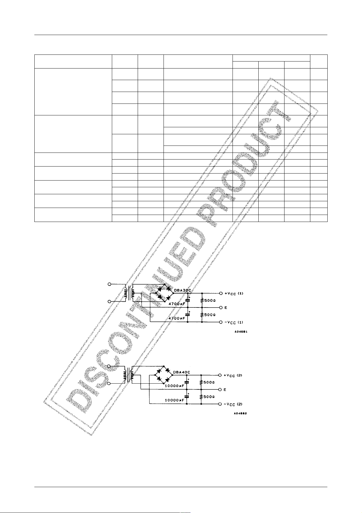
Operating Characteristics at Ta = 25˚C, RL=6Ω (noninductive load), Rg=600Ω, VG=40dB
retemaraPlennahClobmySsnoitidnoC
V
R,LP
rewoptuptuO
noitrotsidcinomrahlatoT
esnopserycneuqerF
ecnadepmitupnI
egatlovesiontuptuO
tnerructnecseiuQ
egatlovlartueN
CP
R,LP
CP
R,L1DHT
C2DHT
R,Lf
Cf
R,Lr
Cr
R,LV
CVON2V
R,LI
CI
R,LV
CV
1
O
2
O
3
O
4
O
Lf,H
Lf,H
1V
i
2V
i
ON
OCC
OCC
1VCCV03±=07– 007+Vm
N
2VCCV93±=07– 007+Vm
N
CC
%4.0=DHT
V
CC
%4.0=DHT
V
CC
RL3= Ω
V
CC
RL3= Ω
V
CC
POW0.1=
V
CC
V
CC
POW0.1=
V
CC
1V
CC
2V
CC
CC
CC
1V
CC
CC
1VCCV03±=0206001Am
2VCCV93±=010305Am
P,V52±=
O
P,V23±=
O
k01=gR,V03±= Ω 2.1smrVm
k01=gR,V93±= Ω 2.1smrVm
,zHk02otzH02=f,V52±=
,zHk02otzH02=f,V23±=
,%0.1=DHT,zHk1=f,V12±=
,%0.1=DHT,zHk1=f,V62±=
,zHk02otzH02=f,V52±=
P,zHk1=f,V52±=
W0.5=20.0%
O
,zHk02otzH02=f,V23±=
P,zHk1=f,V23±=
W0.5=10.0%
O
+0
dB
,W0.1=k05ot02zH
–3
+0
dB
,W0.1=k05ot02zH
–3
P,zHk1=f,V52±=
W0.1=55kΩ
O
P,zHk1=f,V23±=
W0.1=55kΩ
O
nimpytxam
5203W
0555W
5203W
0555W
Note.
All tests are measured using a constant-voltage supply unless otherwise specified.
Available time for load short-circuit and output noise voltage are measured using the transformer supply specified below.
The output noise voltage is the peak value of an average-reading meter with an rms value scale (VTVM). A regulated AC supply (50Hz) should be used
to eliminate the effects of AC primary line flicker noise.
sgnitaR
tinU
4.0%
4.0%
Specified Transformer Supplies
(L, R ch : RP-25 or Equivalent)
(C ch : MG-200 or Equivalent)
No.5247–2/8
Page 3
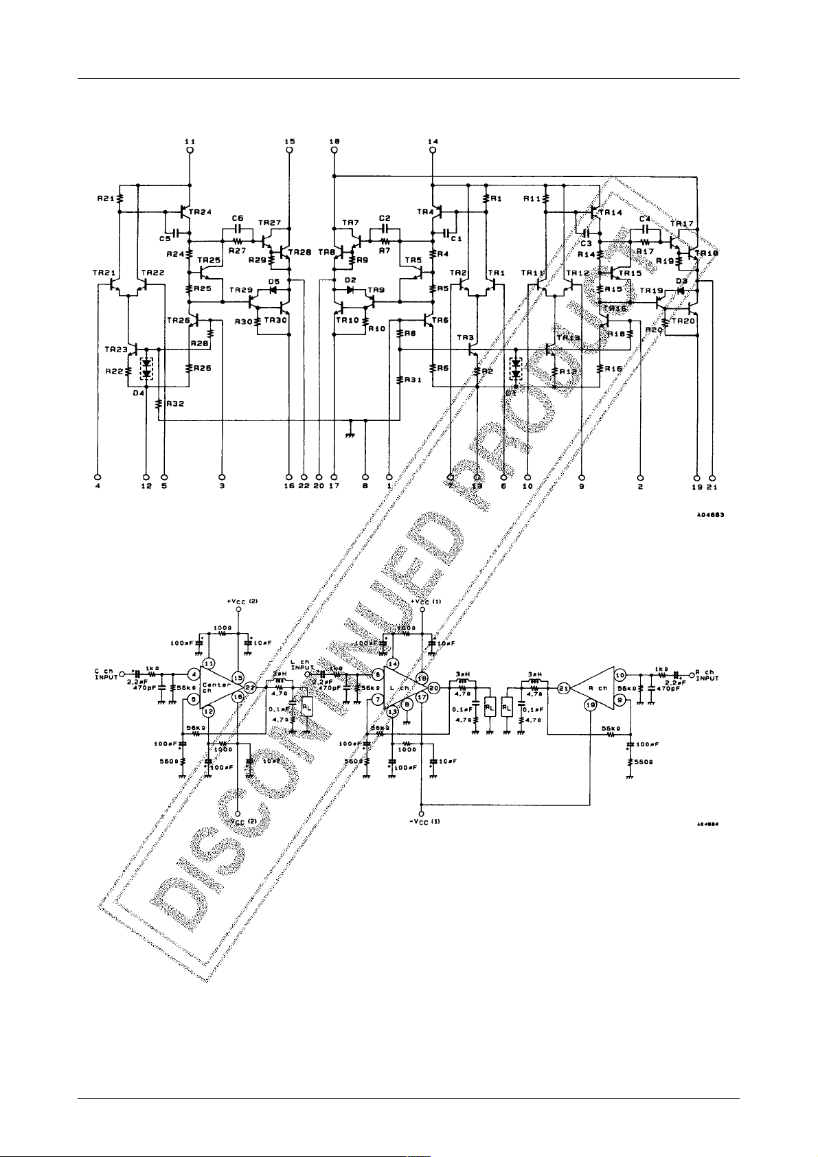
Equivalent Circuit
STK400-490
Sample Application Circuit
No.5247–3/8
Page 4
STK400-490
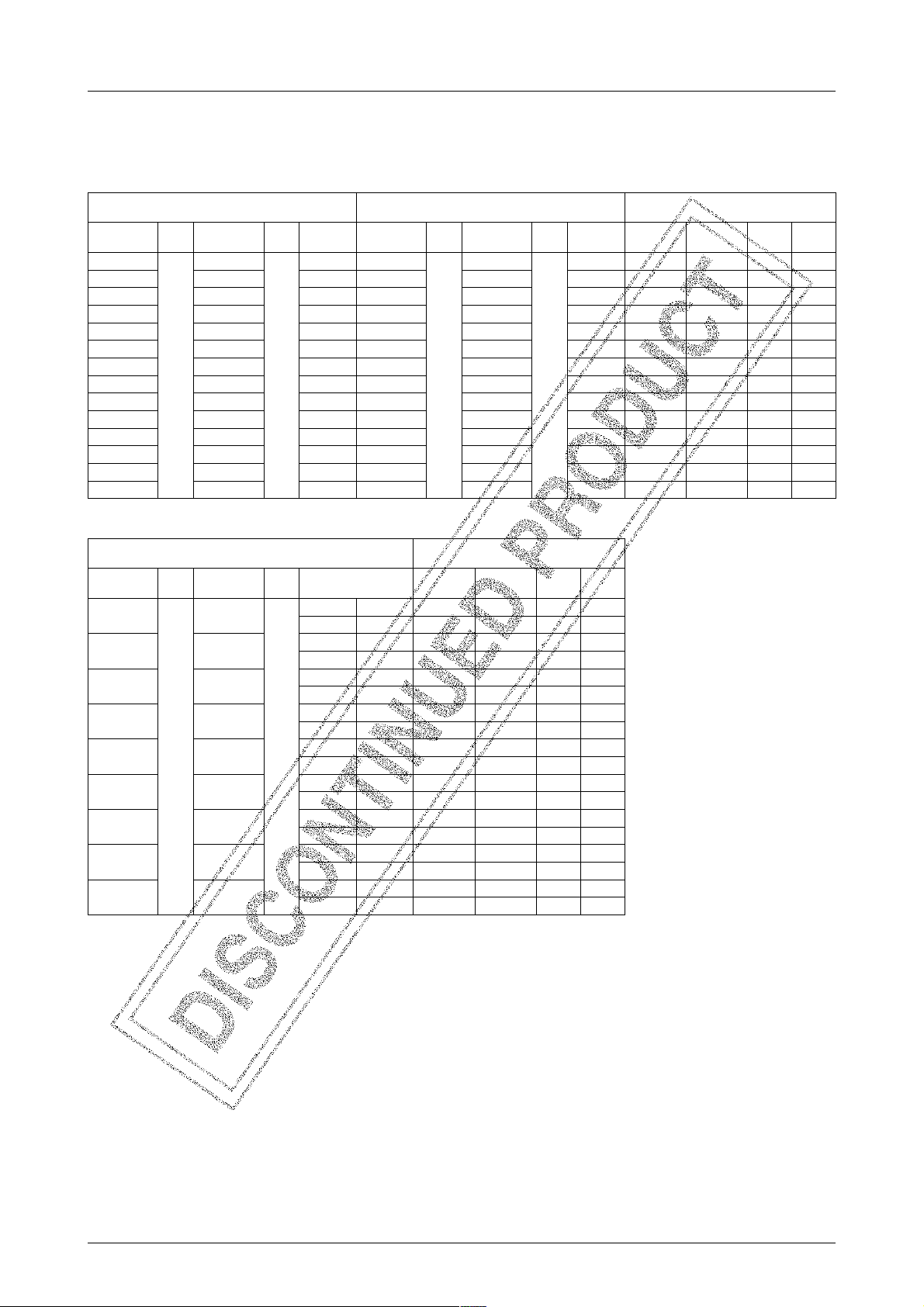
Series Configuration
These devices form a series of pin-compatible devices with different number of output channels, output ratings and total
harmonic distortion. Some of these devices are under development. Contact your San yo sales representati ve if you requiere
more detailed information.
seires002-004KTS,000-004KTS
)gnitartuptuoemas,lennahc-3(
DHT
.oNepyT
]%[
010-004KTS
020-004KTS022-004KTSW51 ×3020-104KTS022-104KTSW51 ×2- 0.92±0.02±0.61±
030-004KTS032-004KTSW02 ×3030-104KTS032-104KTSW02 ×2- 0.43±0.32±0.91±
040-004KTS042-004KTSW52 ×3040-104KTS042-104KTSW52 ×2- 0.63±0.52±0.12±
050-004KTS052-004KTSW03 ×3050-104KTS052-104KTSW03 ×2- 0.93±0.62±0.22±
060-004KTS062-004KTSW53 ×3060-104KTS062-104KTSW53 ×2- 0.14±0.82±0.32±
070-004KTS072-004KTSW04 ×3070-104KTS072-104KTSW04 ×2- 0.44±0.03±0.42±
4.0
080-004KTS082-004KTSW54 ×3080-104KTS082-104KTSW54 ×2- 0.54±0.13±0.52±
090-004KTS092-004KTSW05 ×3090-104KTS092-104KTSW05 ×2- 0.74±0.23±0.62±
001-004KTS003-004KTSW06 ×3001-104KTS003-104KTSW06 ×2- 0.15±0.53±0.72±
011-004KTS013-004KTSW07 ×3011-104KTS013-104KTSW07 ×20.65±-0.83±-
DHT
.oNepyT
]%[
012-004KTS
80.0
detaR
tuptuo
W01 ×3010-104KTS
DHT
.oNepyT
]%[
4.0
021-104KTS023-104KTSW08 ×20.16±-0.24±031-104KTS033-104KTSW001 ×20.56±-0.54±041-104KTS043-104KTSW021 ×20.47±-0.15±-
)lennahc-2(
.oNepyT
seires002-104KTS,000-104KTS
DHT
]%[
012-104KTS
80.0
detaR
V
1xamVCC2xamVCC1VCC2
CC
tuptuo
W01 ×2- 0.62±5.71±0.41±
1]V[egatlovylppuS
seires006-004KTS,004-004KTS
)sgnitartuptuotnereffid,lennahc-3(
DHT
.oNepyT
]%[
054-004KTS
064-004KTS066-004KTS
074-004KTS076-004KTS
084-004KTS086-004KTS
4.0
094-004KTS096-004KTS
005-004KTS007-004KTS
015-004KTS017-004KTS
025-004KTS027-004KTS
035-004KTS037-004KTS
DHT
.oNepyT
]%[
056-004KTS
80.0
detaR
tuptuo
hcCW03- 0.93±0.62±0.22±
hcR,hcLW51- 0.92±0.02±0.61±
hcCW53- 0.14±0.82±0.32±
hcR,hcLW51- 0.92±0.02±0.61±
hcCW04- 0.44±0.03±0.42±
hcR,hcLW02- 0.43±0.32±0.91±
hcCW54- 0.54±0.13±0.52±
hcR,hcLW02- 0.43±0.32±0.91±
hcCW05- 0.74±0.23±0.62±
hcR,hcLW52- 0.63±0.52±0.12±
hcCW06- 0.15±0.53±0.72±
hcR,hcLW03- 0.93±0.62±0.22±
hcCW070.65±-0.83±-
hcR,hcLW53- 0.14±0.82±0.32±
hcCW080.16±-0.24±-
hcR,hcLW04- 0.44±0.03±0.42±
hcCW0010.56±-0.54±-
hcR,hcLW05- 0.74±0.23±0.62±
V
1xamVCC2xamVCC1VCC2
CC
1. VCC max1 (RL=6Ω), VCC max2 (RL=3 to 6Ω), VCC1 (RL=6Ω), VCC2 (RL=3Ω)
1]V[egatlovylppuS
No.5247–4/8
Page 5

STK400-490
Heatsink Design Considerations
The heatsink thermal resistance, θc-a, required to dissipate
the STK400-490 device total power dissipation, Pd, is determined as follows :
Condition 1: IC substrate temperature not to exceed 125°C
Pd (total)×θc-a+Ta<125°C .................................(1)
Pd (total)=Pd (L)+Pd (R)+Pd (C)
Where Ta is the guaranteed maximum ambient temperature, Pd (total) is the total power dissipation, Pd (L) is the
left-channel power dissipation, Pd (R) is the right-channel
power dissipation and Pd (C) is the center-channel power
dissipation.
Condition 2: Power transistor junction temperature, Tj, not
to exceed 150°C
Pd (total)×θc-a+[Pd (L)+Pd (R)]/N
×θj-c+Ta<150°C ................................................. (2)
Pd (total)×θc-a+Pd (C)/N’
×θj-c’+Ta<150°C................................................ (3)
where N is the left and right-channel number of power transistors, N’ is the center-channel number of power transis-
tors, θj-c is the left and right-channel power transistor thermal resistance per transistor, and θj-c’ is the center-chan-
nel power transistor thermal resistance per transisttor . Note
that the power dissipated per transistor is the total, Pd,
devided evenly among the N power transistors.
When estimating the power dissipation for an actual audio
signal input, the rule of thumb is to select Pd corresponding to (1/10) × P
max (within safe limits) for a continuous
O
sine wave input. For example,
Pd (L)+Pd (R)=25W [for (1/10) × P
Pd (C)=21.6W [for (1/10) × P
O
max=5W]
O
max=2.5W]
Pd (total)=Pd (L)+Pd (R)+Pd (C)=46.6W
The STK400-490 has 4 left + right-channel power transistors (N), 2 center-channel power transistors (N’), left + rightchannel thermal resistance per transistor (θj-c) is 2.1°C/W,
and center-channel thermal resistance per transistor (θj-c’)
is 1.7°C/W. If the guaranteed maximum ambient temperature, Ta, is 50°C, then the required heatsink thermal resistance, θc-a, is :
From expression (1)’ :
θc-a < (125–50)/46.6
< 1.60
From expression (2)’ :
θc-a < (150–50)/46.6–25×2.1/(46.6×4)
< 1.86
From expression (3)’ :
θc-a < (150–50)/46.6–21.6×1.7/(46.6×2)
< 1.75
Therefore, to satisfy all three expressions, the required
heatsink must have a thermal resistance less than 1.6°C/W.
Expressions (1), (2) and (3) can be rewritten making θc-a
the subject.
θc-a< (125–Ta)/Pd (total)................................. (1)’
θc-a< (150–Ta)/Pd (total)–[Pd (L)+Pd (R)]
×θj-c/[Pd (total)×N].......................................... (2)’
θc-a< (150–Ta)/Pd (total)–Pd (C)×
θj-c’/[Pd (total)×N’] ......................................... (3)’
The heatsink required must have a thermal resistance that
simultaneously satisfies all three expressions.
The heatsink thermal resistance can be determined from
(1)’, (2)’ and (3)’ once the following parameters have been
defined.
• Supply voltage : V
• Load resistance : R
CC
L
• Guaranteed maximum ambient temperature : Ta
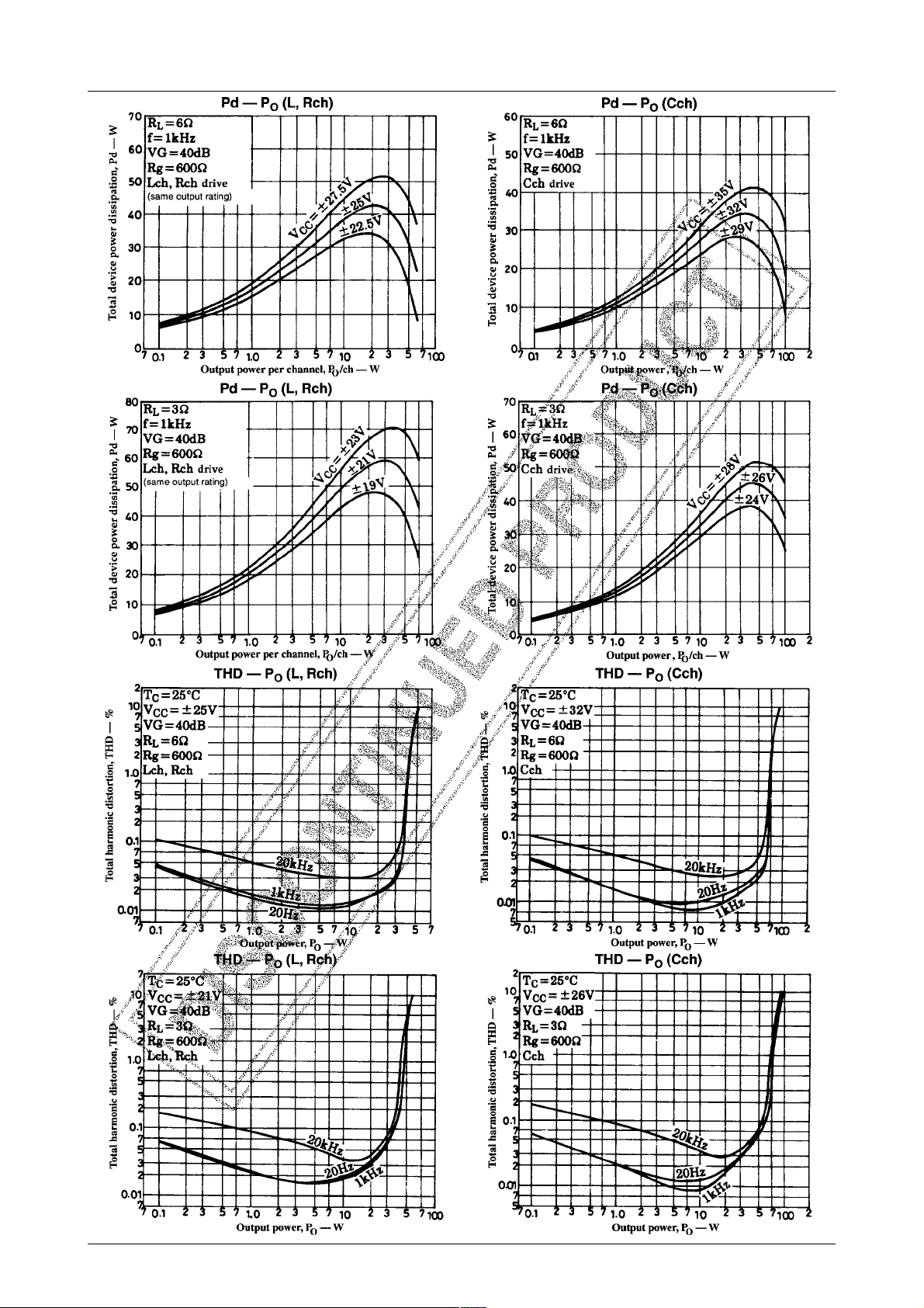
The total device power dissipation when STK400-490
(1)=±25V , V
V
CC
(2)=±32V and RL=6Ω, for a con-
CC
tinuous sine wave signal, is a maximum of 42.5W
(left+righ channels) and 34.3W (center channel), as
shown in the “Pd–P
” characteristics graphs.
O
Similarly, when STK400-490 V
(1)=±21V, V
CC
CC
(2)=±26V and RL=3Ω,
Pd (L)+Pd (R)=30W [for (1/10) × P
Pd (C)=25.5W [for (1/10) × P
O
max=5W]
O
max=2.5W]
Pd (total)=Pd (L)+Pd (R)+Pd (C)=55.5W
From expression (1)’ :
θc-a < (125–50)/55.5
< 1.35
From expression (2)’ :
θc-a < (150–50)/55.5–30×2.1/(55.5×4)
< 1.51
From expression (3)’ :
θc-a < (150–50)/55.5–25.5×1.7/(55.5×2)
< 1.41
Therefore, to satisfy all three expressions, the required
heatsink must have a thermal resistance less than 1.35°C/
W.
This heatsink design example is based on a constant-voltage supply, and should be verified within your specific set
environment.
No.5247–5/8
Page 6
STK400-490
No.5247–6/8
Page 7
STK400-490
No.5247–7/8
Page 8
STK400-490
Specifications of any and all SANYO products described or contained herein stipulate the performance,
characteristics, and functions of the described products in the independent state, and are not guarantees
of the performance, characteristics, and functions of the described products as mounted in the customer's
products or equipment. To verify symptoms and states that cannot be evaluated in an independent device,
the customer should always evaluate and test devices mounted in the customer's products or equipment.
SANYO Electric Co., Ltd. strives to supply high-quality high-reliability products. However, any and all
semiconductor products fail with some probability. It is possible that these probabilistic failures could
give rise to accidents or events that could endanger human lives, that could give rise to smoke or fire,
or that could cause damage to other property. When designing equipment, adopt safety measures so
that these kinds of accidents or events cannot occur. Such measures include but are not limited to protective
circuits and error prevention circuits for safe design, redundant design, and structural design.
In the event that any or all SANYO products(including technical data,services) described or
contained herein are controlled under any of applicable local export control laws and regulations,
such products must not be exported without obtaining the export license from the authorities
concerned in accordance with the above law.
No part of this publication may be reproduced or transmitted in any form or by any means, electronic or
mechanical, including photocopying and recording, or any information storage or retrieval system,
or otherwise, without the prior written permission of SANYO Electric Co. , Ltd.
Any and all information described or contained herein are subject to change without notice due to
product/technology improvement, etc. When designing equipment, refer to the "Delivery Specification"
for the SANYO product that you intend to use.
Information (including circuit diagrams and circuit parameters) herein is for example only ; it is not
guaranteed for volume production. SANYO believes information herein is accurate and reliable, but
no guarantees are made or implied regarding its use or any infringements of intellectual property rights
or other rights of third parties.
This catalog provides information as of September, 1999. Specifications and information herein are
subject to change without notice.
PS No.5247–8/8
 Loading...