

SANYO SM-29-C5DTR Service Manual FC3-A
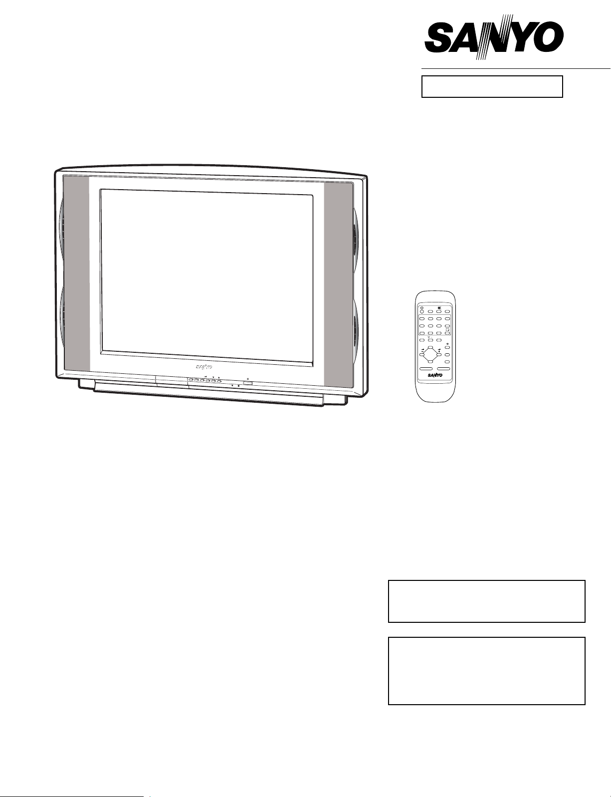
SERVICE MANUAL Colour Television
Specifications
Power Source . . . . . . . . . . AC110-240V, 50Hz/60Hz.
Colour System . . . . . . . . . PAL/SECAM/NTSC4.43/NTSC/PAL-60Hz
Television System . . . . . . B/G, D/K, K’, I, M/M
Channel Coverage . . . . . VHF: E2-E12, R1-R12, K1-K9, A2-A13, J1-J12
UHF: 21-69, A14-A69, J13-J62
CATV: S1-S41, X, Y, Z, Z+1, Z+2
Video IF . . . . . . . . . . . . . . 38.0MHz
Aerial Input Impedance . . 75Ω
Ext. Terminals
Video inputs: Phono jack x 2 (1Vp - p, 75Ω)
S-Video inputs: Din 4 pin x 1 (Separate Y/C signal input)
Audio inputs: Phono jack (L/R) x 2 (436mVrms, more than 40KΩ)
Video monitor outputs: Phono jack x 1 (1Vp - p, 75Ω)
Audio monitor outputs: Phono jack (L/R) x 1 (436mVrms, less than 600Ω)
Headphone jack: Mini stereo jack x 1
Speaker . . . . . . . . . . . . . . 8 cm x 13cm x 2 pcs.
Sound Output (RMS) . . . . 5W + 5W
Dimensions . . . . . . . . . . . 816 (W) x 583 (H) x 504 (D)mm
Weight . . . . . . . . . . . . . . . . approx. 46.7 Kg
Specifications subject to change without notice.
Product Code: 111363315
Original Version
Chassis Series: FC3-A
C5DTR
FILE NO.
Model No. CE29KF8R
Service Ref. No. CE29KF8R-00
(Russia)
Give complete “SERVICE REF. NO.” for
parts order or servicing. It is shown on the
rating plate at the cabinet back of the unit.
This T.V. receiver will not work properly in
foreign countries where the television
transmission system and power source differ from the design specifications. Refer to
the specification table.
TV/AV
MENU
+
-
P
TV/AV
TIMER
14
7
85236
-/--
0
9
A B
BASS
SURROUND
PP
P▲
CH SCAN
SWAP
P▼
MENU
PIC MODE
JXMYA
Contents
-2-
Safety Notice
SAFETY PRECAUTIONS
1: An isolation transformer should be connected in the
power line between the receiver and the AC line
when a service is performed on the primary of the
converter transformer of the set.
2: Comply with all caution and safety-related notes pro-
vided on the cabinet back, inside the cabinet, on the
chassis or the picture tube.
3: When replacing a chassis in the cabinet, always be
certain that all the protective devices are installed
properly, such as, control knobs, adjustment covers
or shields, barriers, isolation resistor-capacitor networks etc.. Before returning any television to the
customer, the service technician must be sure that
it is completely safe to operate without danger of
electrical shock.
X-RADIATION PRECAUTION
The primary source of X-RADIATION in television receiver is the picture tube. The picture tube is specially constructed to limit X-RADIA TION emissions. For continued X-RADIATION protection, the replacement tube must be
the same type as the original including suffix letter. Excessive high voltage may produce potentially hazardous X
- RADIATION. To avoid such hazards, the high voltage must be maintained within specified limit. Refer to this
service manual, high voltage adjustment for specific high voltage limit. If high voltage exceeds specified limits,
take necessary corrective action. Carefully follow the instructions for + B1 volt power supply adjustment, and high
voltage check to maintain the high voltage within the specified limits.
PRODUCT SAFETY NOTICE
Product safety should be considered when a component replacement is made in any area of a receiver.
Components indicated by mark in the parts list and the schematic diagram designate components in which
safety can be of special significance. It is particularly recommended that only parts designated on the parts list
in this manual be used for component replacement designated by mark . No deviations from resistance
wattage or voltage ratings may be made for replacement items designated by mark .
Safety Notice . . . . . . . . . . . . . . . . . . . . . . . . . . . . . . . . . . . . . . . . . . . . . . . . . . . . . . . . . . . . . . . . . . . . . . . . . . . 2
Chassis Block Diagram . . . . . . . . . . . . . . . . . . . . . . . . . . . . . . . . . . . . . . . . . . . . . . . . . . . . . . . . . . . . . . . . . . 3-4
IC Block Diagrams . . . . . . . . . . . . . . . . . . . . . . . . . . . . . . . . . . . . . . . . . . . . . . . . . . . . . . . . . . . . . . . . . . . . . 5-8
Mechanical Disassemblies . . . . . . . . . . . . . . . . . . . . . . . . . . . . . . . . . . . . . . . . . . . . . . . . . . . . . . . . . . . . . . . . . 9
Service Information . . . . . . . . . . . . . . . . . . . . . . . . . . . . . . . . . . . . . . . . . . . . . . . . . . . . . . . . . . . . . . . . . . . . . . 9
Service Adjustments with replacing Memory IC (IC802) . . . . . . . . . . . . . . . . . . . . . . . . . . . . . . . . . . . . . . 10-13
Service Mode Adjustments . . . . . . . . . . . . . . . . . . . . . . . . . . . . . . . . . . . . . . . . . . . . . . . . . . . . . . . . . . . . . 14-15
Service Adjustments . . . . . . . . . . . . . . . . . . . . . . . . . . . . . . . . . . . . . . . . . . . . . . . . . . . . . . . . . . . . . . . . . . . . 16
Special Function . . . . . . . . . . . . . . . . . . . . . . . . . . . . . . . . . . . . . . . . . . . . . . . . . . . . . . . . . . . . . . . . . . . . . . . .17
Purity and Convergence Adjustment . . . . . . . . . . . . . . . . . . . . . . . . . . . . . . . . . . . . . . . . . . . . . . . . . . . . . 18-19
Cabinet Parts List . . . . . . . . . . . . . . . . . . . . . . . . . . . . . . . . . . . . . . . . . . . . . . . . . . . . . . . . . . . . . . . . . . . . . . . 20
Chassis Electrical Parts List . . . . . . . . . . . . . . . . . . . . . . . . . . . . . . . . . . . . . . . . . . . . . . . . . . . . . . . . . . . . 21-30
-3-
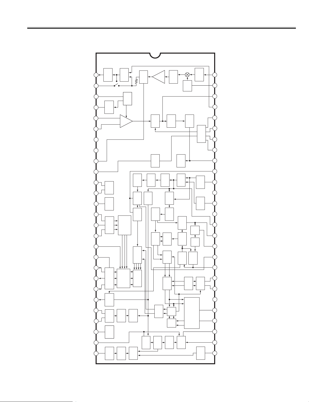
Chassis Block Diagrams
MAIN SIGNAL PROCESSING CIRCUIT
HV
CRT
DY
L902
HV
TUNER
5V-1
CRT UNIT
LED
D1910
A1901A
RC RECEIVER
KEYS
FRONT
SW1901~
CONTROL
IC701
OUTPUT AMP.
TRIPLE VIDEO
SW1906
G
R
9
8
2
1
G
R
ON-TIMER
32
RC-IN
28
IC801
12
KEY-IN
B
B
7
3
CPU
HEATER
4
3
21
20
19
2/5
5
IC501
1
SCL
6
5
SDA
Q432
H-OUT
VERT. /DEF.
IC802
EEPROM
OSD B-OUT
OSD G-OUT
OSD R-OUT
T431
TRANS.
H-DRIVE
OSD R-IN
IC201
IF/VIDEO/CHROMA
FOCUS
SCREEN
FBT
T471
Q431
OSD G-IN
OSD B-IN
15
14
5/6
IF IN
H-DRIVE
R-OUT
19
16
42
VIDEO/
(S-Y) IN
PCC
CIRCUIT
Q461-Q462
G-OUT
B-OUT
21
20
MATRIX
RGB
46
VIDEO OUT
VERT. OUT
23
44
S-C IN
HORIZ. OUT
27
52
SIF OUT
54
SIF IN
POWER SUPPLY CIRCUIT
T611
CONVERTER
2
FM OUT
(TV OUT)
36V
Reg.
TRANS.
FBT
140V
VR631
+B Adj.
13
1H
DL
VERT. DEF./HORIZ. DEF.
Reg.
24V
14
35
R-Y
IC281
SECAM
CPU/EEPROM
5VRC
IC681
6
AUDIO CTL/AV SW
15
34
B-Y
7
IC202
IC201
9V
17
SWITCH
14
Reg.
AUDIO AMP.
28V
SAW
X161A
A101
FILTER
TUNER
K001
IC3702
L/R, L/L,R/R SW
15
L
1
IC3701
SURROUND
AUDIO CONTROL /
23
R
4
IC001
7
AUDIO AMP.
R-OUT
JACK
HEADPHONE
SP902
R
1/3
4
30
8
L
2
12
L-OUT
SP901
IC1501
VIDEO SW
IC1401
VIDEO-SW
9
AV1 VIDEO IN
4
3
5
INT . VIDEO
15
1
2
EXT.
VIDEO
4
6
Y-IN
7
1
C-IN
EXT . VIDEO
14
13
12
Y
AV2 VIDEO IN
C-IN
INPUT TERMINAL
REAR AV1
Y-IN
OUT
VIDEO
MONITOR
IC1201
AUDIO-SW
VIDEO IN
S-TERMINAL
1/5
12/14
2
15
AV1
AV1
AUDIO IN (RIGHT)
AUDIO IN (LEFT)
L-OUT
3
FRONT
R-OUT
13
VIDEO IN
AV2
INPUT TERMINAL
AV2
AUDIO IN (LEFT)
VIDEO IN
4
11
AV2
AUDIO IN (RIGHT)
VIDEO MONITOR OUT
AUDIO MONITOR OUT(RIGHT)
AUDIO MONITOR OUT(LEFT)
-4-
Chassis Block Diagrams
SYSTEM CONTROL
QXXAVC321P
&
IC3701
SURROUND
AUDIO CONTROL
17
13 14
18
A101
F/S TUNER
CIRCUIT
DEFLECTION
IC201
11 12
etc.
KEY
SWITCH
KEY SWITCH IN
12
29
50/60Hz OUTPUT (60Hz=LOW, 50Hz=HIGH)
30
23
9
10
IC3702
SWITCH
L/R, L/L, R/R
S-TERMINAL INPUT (S-IN=LOW)
34
CPU
IC801
QXXAVC044P
SCL
2
SDA
1
24
PHOTO COUPLE
POWER ON/OFF
(ON=HIGH, OFF=LOW)
31
26
13
33
IF/VIDEO / CHROMA/DEF.
AFT SIGNAL INPUT
OSD BLK OUT(Active=High)
22
10
28
OSD BLUE OUT(Active=High)
OSD GREEN OUT(Active=High)
OSD RED OUT(Active=High)
19
20
32
211817
6
POWER CIRCUIT
HORIZ. SYNC IN (ACTIVE=LOW)
VERT. SYNC IN (ACTIVE=LOW)
POWER PROTECT IN
(POWER ERROR=LOW)
27
34
SDA
SCL
56
IC802
MEMORY
7
MUTE OUTPUT
(MUTE ON=HIGH)
AV1/AV2 SWITCH
(AV1=LOW, AV2=HIGH)
11
IC001
10
IC1201
AUDIO AMP.
(AV1=LOW,
9
AV2=HIGH)
8
TV/AV SWITCH
(TV=LOW,
AV=HIGH)
IC1401
AUDIO SWITCH
(Y =LOW,
AV VIDEO=HIGH)
3
(INT. VIDEO =LOW,
(Y =LOW,
AV VIDEO=HIGH)
11
IC1501
VIDEO SWITCH
EXT. VIDEO=HIGH)
RESET INPUT (ACTIVE=LOW)
10
SECAM KILLER INPUT (HIGH=SECAM)
VIDEO SWITCH
(ON TIMER ON=Low)
RC SIGNAL IN
(ACTIVE=HIGH)
ON-TIMER LED OUT
RC PRE-AMP.
VIF-M OUTPUT (HIGH=NTSC3.58, LOW=OTHER)
LED
CPU OSC OUT
CPU OSC IN
OSC
X801
32.768KHz
-5-
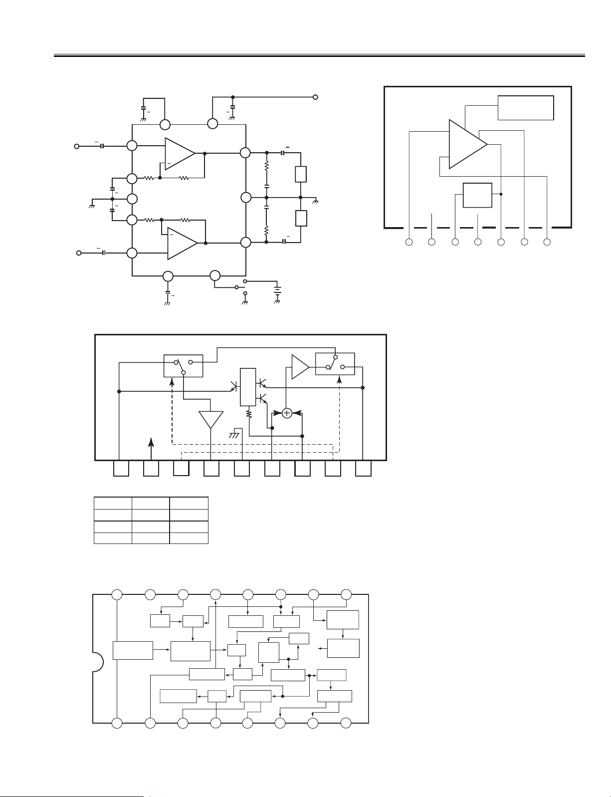
IC Block Diagrams
IC201 < IF/Video/Chroma/Def. > LA76818J-E
Audio Output
FM Output/Selected
Audio Output
PIF AGC
RF AGC Output
PIF Input1
PIF Input 2
IF Ground
IF Vcc
FM Filter
AFT Output
Bus Data
Bus Clock
ABL
Red Input
Green Input
Blue Input
Fast Blanking Input
RGB Vcc
Red Output
Green Output
Blue Output
fsc output or C
Sync output
Vertical Output
Ramp ALC Filter
Horizontal/BUS Vcc
Horizontal AFC Filter
Horizontal Output
VOL
DC
1
2
3
AGC
RF
4
56
7
VCC 5V
IF
8
9
10
11
BUS
12
ABL
13
14
CLAMP
15
16
17
18
VCC
19 20
DRIVE/OUT-OFF
21
SYNC SW
FSC/
22
23
RAMP
VER
24
HOR
VCC
25
VCC
H
26 27
HOR
OUT
SW
AGC
IF
VIF
CONTRAST
BRIGHT
OSD
OSD
SW
VER
C/D
SHIFTER
PHASE
VER
SEP
AFC2
CORING
STRETCH
REST
BRIGHT
MATRIX
DET
FM
PEAKING
LINE
SYNC
BLACK
SEP
DC
CONTRAST
RGB
AFC1
VIDEO
DET
AFT
DELAY
ACC
DEMO
CLAMP
C/D
AMP
LIM
TRAP
SW
CLAMP
SW
COLOR
HOR
BPF
TRAP
SW
ON/OFF
BPF
PAL
+
ALC
LPF
1/256
IDENT
IF
VIDEO
SW
APC1
TINT
VCO
HOR
VCO
SPLL
VIDEO
AMP
APC2
DC ADS.
1H DELAY
VXO
DDS
BPF
A2C
PLL
CLMP
CLMP
CLAMP
FBP
SIF Input
SIF APC Filter
525354
SIF Output
51
Ext. Audio Input
APC Filter
4950
VCO Coil 1
48
VCO Coil 2
47
VCO Filter
46
Video Output
Black Level Detector
4445
Internal Video Input (S-C IN)
V/C VCC
43
5V
Video/Vertical Vcc
42
External Video Input(Y-IN)
41
Video/Vertical/BUS Ground
40
Selected Video Output
39
Chroma APC1 Filter
38
4.43 MHz Crystal
Clamp Filter
Chroma APC2 Filter
353637
SECAM R-Y Input
(Cr Input)
34
SECAM B-Y Input
(Cb Input)
33
CCD/Horizontal Ground
32
CCD Filter
31
VCC
CCD Vcc
1H
30
Clock (4MHz) Outupt
VCO IREF
2829
Flyback Pulse Input
IC Block Diagrams
-6-
IC201 <IF System Block Diagram> LA76818J-E
1K
SIF
APC
1000p
0.01u
Filter
10p
SIF.In
SIF.Out
Deem-TC
FM Gain
LIM
AMP
53
500K
54
52
1bit
1bit
FM
500K
Det
Amp
Sound
Det
Snd
FM
Det
BPF
BPF
Out
2
De-
Amp
+
Amp
emph
-
FM.Level
SIF
VCO
0.01u
5bit
pre-
SIF. Sys
+
9
-
+
scaller
2bit
FM
Filter
1u
1 bit
FM Mute
2.5V
C/D
Chroma
Det
APC
C/D
OSC
Out
Video
Sound
Det
Video
46
Amp
Trap
+
10u
Audio in
51
To
BUS
IF
Ident
B/N
INV
Video.Level
Audio.out
1
(ATT)
VOLUME
Input
Select
3bit
1bit
A.Fil.Def
Filter
VOLUME
1bit
A.SW
VCO
Chroma
7bit
VOLUME
D/A
VOLUME
1bit
A.MUTE
Buzz
Canceller
Lock
47
Det
VCO
Filter
+
VCO
VCO
VIF
-π/4
0.47u
Alignment
Phase
Detector
Ident
VIF.Sys
Reset
Counter
To
BUS
+π/4
Vcc
2bit
Pulse
AFT
100K
10
AFT
Chroma
Counter
VIF
VCO
PLL Pull-in SW
Det
APC
0.1u
100K
49
48
50
VCO
COIL2
VCO
COIL1
APC
Filter
330
VCO.Coil
+
0.47u
Clock
Data
12
11
to BUS Line
BUS
Interface
VIF AMP
5
In1
PIF
IF In
VIF 3
VIF 2
VIF 1
SAW
6
In2
PIF
Drive
IF AGC
9V
IF
2ndIF
RF
30K
AGC
AGC
AGC
4
+
Out
RF AGC
RF AGC
120K
Delay
6bit
Def
IF AGC
1bit
8
IF VCC
PIF
AGC
3
To
BUS
-
+
(6 Vcc)/7
0.022u
7
IF
+
GND
-7-
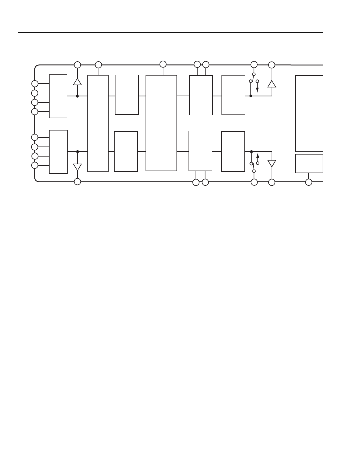
IC Block Diagrams
IC001 < Audio AMP.> TA8200AH
IC281 <SECAM Decoder> LA7642N
IC1401 < VIDEO Switch > MM1188XS
IC501 < Vertical Output > LA78041
++
9
Vcc
OUT 1
PW-GND
OUT 2
11
7
10
12
IN 1
IN 1
+
4
400Ω
5
+
3
+
1
IN 2 IN 2
+
2
Ripple Filter
Pre-GND
400Ω
6
+
AMP.1
AMP.2
+
8
20KΩ
20KΩ
+
SW
Vcc
Thermal
Protection
-
2
Vcc
AMP
+
Pump
Up
3
GND
PUMP UP
OUT
4
5
6
OUTPUT
Ver. OUTPUT
7
NON INV.
ST A GE Vcc
INPUT
+
RL
RL
+
SW
1
INVERTING
INPUT
CLAMP
15K
6dB
3
SW1
OUT
IN 2
IN 3
4
OUT
5
GND6IN1-Y
IN 3
SW1
L
H
-
1
2
Vcc
SW2
L IN 1
L
H
AV/SECAMKil-Out
13
System
SW1
16
Bell/EQU
Adj
VccEQU-Adj
Video In
1415
ACC
SW3
Bell/EQU
Filter
12
CLAMP
BIAS
CLAMP
4.43MHz In
11
PLL
DET
SW2
6dB
(-6dB)
7
IN1-C
VCO
8
SW29IN 2
4MHz InSC-In
10
Pulse
DET
Pulse
I/F
9
1
F0-Fil Kil-Fil
2
KILLER
ID-KIL
3
4.43DC ID-Fil 4M-DC
LIM
ID
4
F0 Adj
5
Filter
6
R-Y Out
Clamp
SW/ALC
7
B-Y Out GND
8
IC Block Diagrams
-8-
IC701 < Triple Video Output Amplifier. > TDA6103Q
IC3701 < Audio Control & Surround > NJW1138MP
IN 1a
IN 2a
IN 3a
IN 4a
IN 1b
IN 2b
IN 3b
IN 4b
30
29
28
27
MONa
5
-2dB
AGC
20
SR-FIL
6
TONE Ha
7
TONE La
8
OUT a
10
LINEa
9
+4.5 dB
1
2
SEL
VOL 1
TONE
VOL 2
3
4
AGC
SEL
-2dB
26
MONb
VOL 1
NJRC
ORIGINAL
SURROUND
&
SIMULATED
STEREO
TONE Hb
TONE
24
23
TONE Lb
VOL 2
21
OUT b
+4.5 dB
22
LINEb
IIC BUS
INTERFACE
BIAS
17
VREF
-9-
Service Information
This TV set has a built-in power supply protection circuit.
It is provided to protect the TV set in case of a power supply circuit malfunctions. When something abnormality occurs
during TV reception, the TV set goes to the stand-by mode.
When an abnormality occurs during TV reception, it causes pin 27 of the CPU to go continually Low (less than
0.75V) for about one second. The CPU detects that this has occurred and outputs the signal from pin 31 to switch
off the power supply lines.
Releasing the protective circuit and restoring power supply
To release the protective circuit and restore power supply, turn the power to the TV set OFF and then ON again via
either the main power switch or the ON-OFF button on the remote control. This will work only if the power supply
trouble was temporary. If there is permanent trouble such as a damaged circuit, power cannot be restored and the
circuit will have to be repaired.
n Protection Circuit
Mechanical Disassemblies
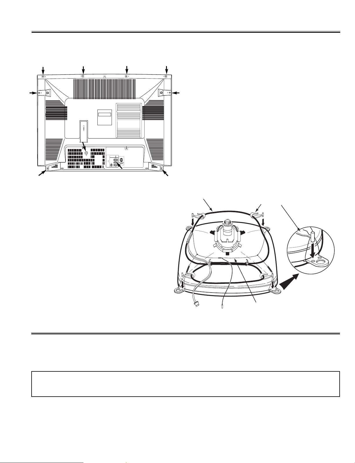
CABINET BACK REMOVAL
1. Refer to Figure 1, remove 10 screws.
2. Pull off cabinet back and remove.
Figure 1. Cabinet Back Removal
CHASSIS REMOVAL
1. Remove cabinet back.
2. Discharge the picture tube anode (2nd anode lead) to the dag
coating (picture tube grounding lead).
3. Disconnect Degaussing coil socket (KE), Picture tube socket,
Deflection yoke connector (KDY), Speaker connectors (K002
and K003), and 2nd anode lead.
4. Remove chassis completely by sliding it straight back.
PICTURE TUBE REMOVAL
CAUTION: Do not disturb the deflection yoke or magnet
assembly on the picture tube neck. Care must be taken
to keep these assemblies intact, unless picture tube is
being replaced . Discharge the picture tube to the coating before handling the tube.
1. Remove chassis, referring to Chassis Removal instructions.
2. Place cabinet’s front face down on the soft surface.
3. Remove the screw on each corner of the picture tube and
GENTLY lift the picture tube out of the cabinet.
4. Install a replacement picture tube in reverse order.
Properly install the degaussing coil and picture tube ground
ing lead on the picture tube. See Figure 2.
Note: If the Picture Tube is being replaced, mount the
Degaussing Coil on the picture tube. See Figure 2.
Figure 2.
Picture Tube Removal
MONITOR
AV1 INPUT
OUT
R
AUDIO
L
S-VIDEO
(MONO)
VIDEO
ANT. 75Ω
DEGAUSSING
COIL
DEGAUSSING
COIL HOLDER
DEGAUSSING
COIL SOCKET
To CRT
unit ground
PICTURE TUBE
GROUND LEAD
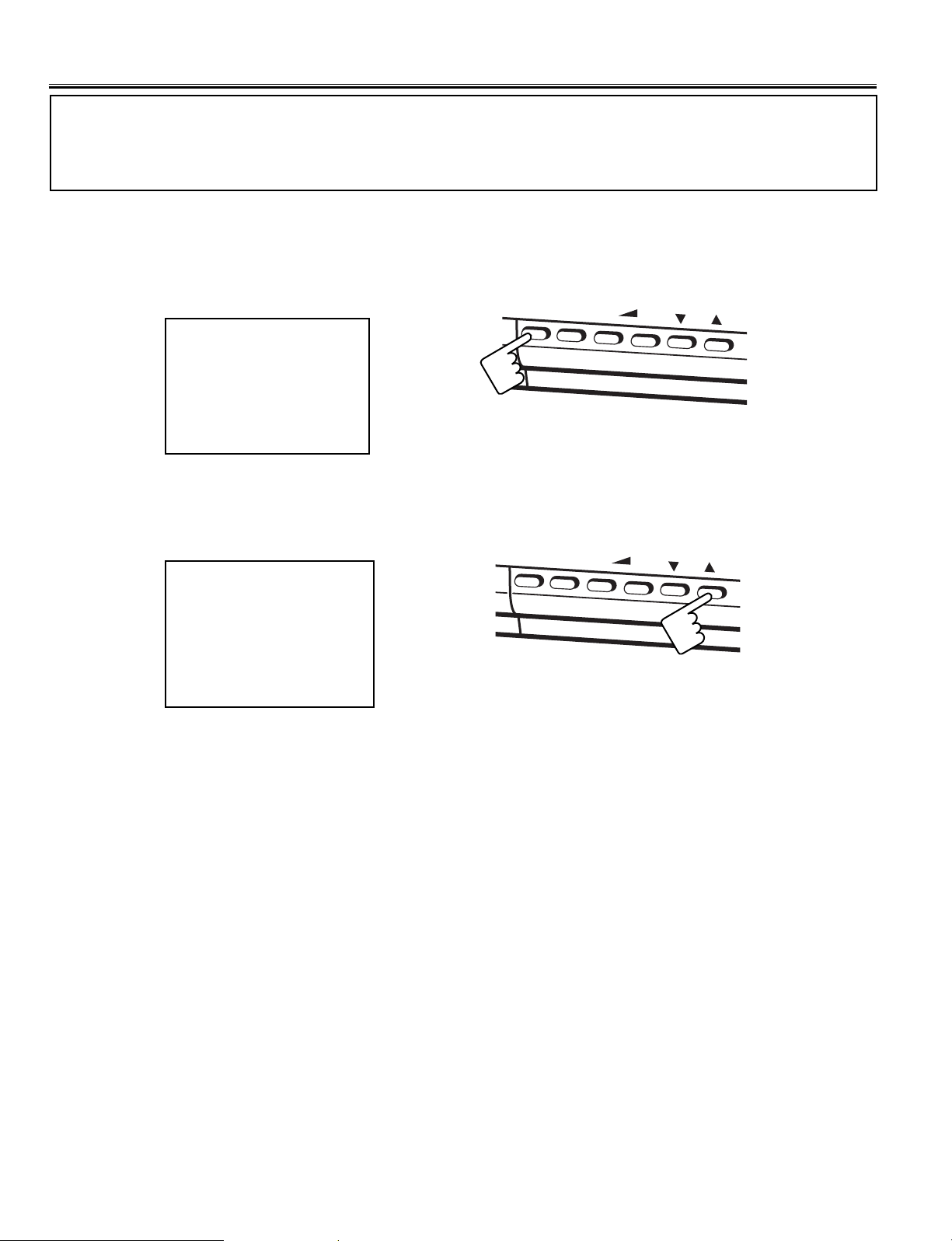
[1] Initializing Procedure
1. Put a new memory IC.
2. Turn on the TV set.
3. Press and hold the TV/AV Selector on the TV set for more than 2 seconds. The following picture appears on the
screen.
4. Press the PROGRAMME UP on the TV set while the above On-Screen Display is still on the screen. The following
picture appears on the screen.
This completes the initialization of memory IC.
Following shows the initialized contents of memory data by this procedure.
- Plug & play : No executed
- Inhibit data : Cancelled
- Ch skip data : Cancelled
- Sound volume data : 10/63 steps.
- Volume Lock : OFF
- Tuning Lock : OFF
- Colour system : AUTO
1
CLR
-10-
Service Adjustments with Replacing Memory IC (IC802)
Note: The CPU (IC801) and memory IC (IC802) store the service adjustments data and controls data for each
circuit. When the Memory IC(IC802) is replaced, some of the service adjustments should be readjusted to
obtain the best performance. The necessary service adjustments are carried out by using the RC handset.
Please set up the TV set with following steps [1] to [2].
Press and hold for more than 2 seconds
TV/AV
MENU
TV/AV
MENU
-
+
-
+
P
P
-11-
Service Adjustments with Replacing Memory IC (IC802)
[2] Required Service Adjustments
Readjust the following service adjustments.
Adjustments Service Mode No. & Item
RF AGC Item 01, RF AGC
Horizontal centre Item 02, H-PHA
Vertical size Item 04, V-SIZ
Vertical-S correction Item 05, V-SCO
Vertical linearity Item 06, V-LIN
Gray scale Item 14-17, 19-21
Further adjustment please refer to page 14 and 15.
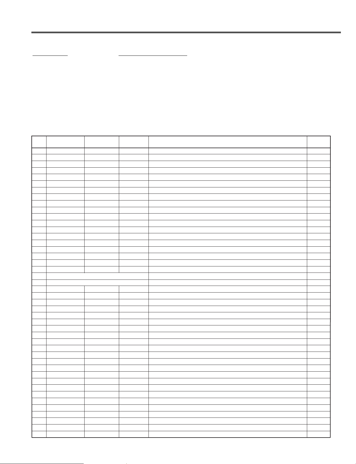
Following table shows the initial values which have been stored in the CPU ROM, and items for the service adjustments.
Service mode adjustments table in CPU ROM
NO.
01
02
03
04
05
06
07
08
09
10
11
12
13
14
15
16
17
18
19
20
21
22
23
24
25
26
27
28
29
30
31
32
33 RBAGN
34
35 BLKS
36
37
38
39
40
41
42
43
44
ITEM
V-SCO
V-LIN 00~31
V-S60
OSDHP
V-SCP
1-LINE APPEAR
DRV
B-YD
R-YD 00~15
B-YDN
R-YDN
SBDC
SRDC
G-YA
RBGB
RBAG
G-YAN
RBGBN
COGV
BLKG
BRTA
BRST
BRTH
PORW
RFCO
DATA
RANGE
00~63
00~31
00~127
00~31
-16~+15
-64~+32
00~255
00~127
00~07
00~07
00~127
00~255
00~255
00~255
00~127
00~15
00~127
00~15
-16~+15
-16~+15
-16~+15
-16~+15
0,1
00~15 8
00~15
0,1
-16~+15
-16~+15
00~03
00~03 3
00~03
0,1
0,1
00~07
00~03
00~03
0,1
00~03
00~03
INITIAL
DATA
30
4
40
71
18
20
+5
0
26
50
7
7
105
0
0
0
64
8
64
9
9
0
0
- 6
- 2
0
8
0
0
0
0
3
0 On and off of ABL. 0=ON, 1=OFF
0
0
2
0
0
2
0
White peak limitter. 0=OFF, 1-3=With LimitterWPL
Y Gamma setting. 0=OFF, 3=Max (Do not change)YGAM
Switching of Pre-shoot and Over shoot in AV mode. 0=Pre, 1=Over
Pre-shoot/Over shoot Adj. in AV mode.PORS
RF Coring Gain Adj.
DESCRIPTION
RF AGC Adj.RF AGC
H-Phase (H-Centering) Adj. (50Hz)H-PHA
V-Position (V-Centering) Adj. (50Hz) Fixed.V-POS 00~63
V-Size Adj. (50Hz)V-SIZ
V-S Correction (50Hz). Strech or shrink at center of screen
V-Linearity Adj. (50Hz)
H-Centering Adj. (60Hz) H-P60
V-Size Adj. (60Hz)
OSD H-Position Adj.
OSD Contrast Adj.OSDC
Correction of the V-size accompanying brightness change.
Correction of the H-size accompanying brightness change.H-SCP
Sub Bias Adj.SBIAS
Red Bias Adj.RBIAS
Green Bias Adj.GBIAS
Blue Bias Adj.BBIAS
Red Drive Adj.RDRIV
Green Drive Adj.GDRIV
Blue Drive Adj.BDRIV
White Balance Adj.
B-Y DC level Adj.. Colour compensation (PAL)
R-Y DC level Adj.. Colour compensation (PAL)
NTSC B-Y DC level Adj. (Difference value from PAL.)
NTSC R-Y DC level Adj. (Difference value from PAL.)
SECAM B-Y DC level Adj. (Difference value from PAL.)
SECAM R-Y DC level Adj. (Difference value from PAL.)
G-Y angle Adj. (Colour Phase G-Y Demodulation 0=240 degree, 1=253 degree)
R-Y, B-Y Gain Blance Adj. (Do not change.)
R-Y, B-Y Angle Adj. (Do not change.)
NTSC G-Y Angle Adj. (Difference value from PAL.)
NTSC R-Y, B-Y Gain Balance Adj. (Difference value from PAL.)
NTSC G-Y, B-Y Angle Adj. (Difference value from PAL)
Coring Adj. (Base colour)
Black stretch effective point selection, 0=OFF, 1-3=FREE
Setting of Black stretch gain. 0=OFF, 1-3=FREE
ABL Effect Limit SW. 0=With Limitter, 1=Without Limitter
ABL Threshold Pint.
(Do not change)
OBJECT
IC201
IC201
IC201
IC201
IC201
IC201
IC201
IC201
IC801
IC201
IC201
IC201
IC201
IC201
IC201
IC201
IC201
IC201
IC201
IC201
IC201
IC201
IC201
IC201
IC201
IC201
IC201
IC201
IC201
IC201
IC201
IC201
IC201
IC201
IC201
IC201
IC201
IC201
IC201
IC201
IC201
IC201
 Loading...