

Page 1
Ordering number : ENN7055B
SGF31
N-Channel GaAs MESFET
SGF31
For C to Ku-band Local Oscillator and Amplifier
Features
•
Lower phase noise.
•
The chip surface is covered with the highly reliable
protection film.
•
Super miniaturized plastic-mold package (CP4).
•
Automatic surface mounting is available.
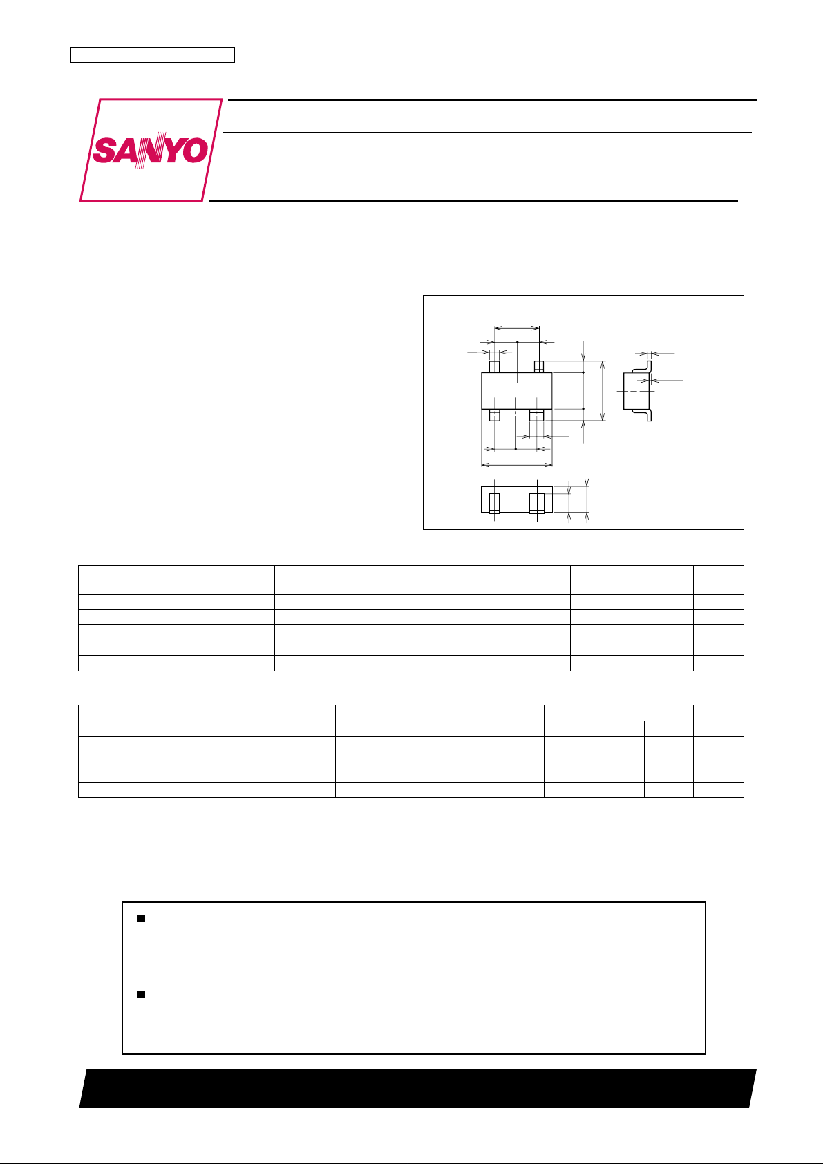
Package Dimensions
unit : mm
2134A
[SGF31]
1.9
0.95
0.4
0.95
43
1
2
0.95
0.85
2.9
0.6
0.8
0.5
1.5
0.5
1.1
0.16
0 to 0.1
2.5
1 : Gate
2 : Source
3 : Drain
4 : Source
SANYO : CP4
Specifications
Absolute Maximum Ratings at Ta=25°C
Parameter Symbol Conditions Ratings Unit
Drain-to-Source Voltage V
Gate-to-Source Voltage V
Drain Current I
Allowable Power Dissipation P
Junction T emperature Tj 150 °C
Storage T emperature T stg --55 to +150 °C
DS
GS
D
D
6V
--5 V
100 mA
200 mW
Electrical Characteristics at T a=25°C
Parameter Symbol Conditions
Gate-to-Source Leakage Current I
Saturated Drain Current I
Gate-to-Source Cutoff Voltage VGS(off) VDS=3V, ID=100µA --0.5 --1.6 --2.7 V
Forward Transfer Admittance
GSO
DSS
yfs
VGS=--5V --10 µA
VDS=3V, VGS=0 30 50 70 mA
VDS=3V, ID=10mA 34 mS
Any and all SANYO products described or contained herein do not have specifications that can handle
applications that require extremely high levels of reliability, such as life-support systems, aircraft's
control systems, or other applications whose failure can be reasonably expected to result in serious
physical and/or material damage. Consult with your SANYO representative nearest you before using
any SANYO products described or contained herein in such applications.
SANYO assumes no responsibility for equipment failures that result from using products at values that
exceed, even momentarily, rated values (such as maximum ratings, operating condition ranges, or other
parameters) listed in products specifications of any and all SANYO products described or contained
herein.
Ratings
min typ max
SANYO Electric Co.,Ltd. Semiconductor Company
TOKYO OFFICE Tokyo Bldg., 1-10, 1 Chome, Ueno, Taito-ku, TOKYO, 110-8534 JAPAN
71502 TS IM / 11802 GI IM / 91001 GI IM
No.7055-1/5
Unit
Page 2
SGF31
S-Parameter
SGF31
FREQUENCY S11 S21 S12 S22
MHz MAG ANG MAG ANG MAG ANG MAG ANG
3000.0000 .671 --120.6 2.964 81.8 .098 34.1 .514 --39.1
4000.0000 .585 --148.0 2.559 61.8 .104 31.2 .441 --52.3
5000.0000 .552 --173.3 2.276 43.0 .114 27.9 .389 --66.5
6000.0000 .550 163.0 2.044 24.7 .131 23.5 .342 --82.7
7000.0000 .573 141.4 1.850 6.8 .154 16.7 .299 --102.3
8000.0000 .611 122.0 1.686 --10.6 .178 7.6 .261 --126.3
9000.0000 .656 104.6 1.541 --27.6 .200 --2.5 .236 --155.4
10000.0000 .702 88.9 1.408 --44.2 .220 --13.0 .235 172.0
11000.0000 .747 74.5 1.284 --60.3 .240 --23.7 .263 140.4
12000.0000 .789 61.1 1.167 --76.1 .260 --35.0 .316 113.3
13000.0000 .827 48.4 1.058 --91.6 .277 --47.0 .384 90.7
14000.0000 .858 35.8 .954 --107.0 .289 --59.5 .457 71.4
15000.0000 .883 23.4 .848 --122.3 .296 --72.0 .533 54.1
16000.0000 .905 11.5 .716 --137.8 .299 --83.6 .625 37.8
VDS=3V IDS=30mA
SGF31
VDS=3V IDS=30mA
FREQUENCY GUmax GAmax S21^2 S12^2 K Delay Mason’s U G1 G2
MHz dB dB dB dB nsec dB dB dB
3000.0000 13.37 9.44 --20.21 .81 .057 20.258 2.60 1.33
4000.0000 10.93 12.95 8.16 --19.66 1.02 .054 18.447 1.82 .94
5000.0000 9.43 10.83 7.15 --18.87 1.13 .052 17.436 1.58 .71
6000.0000 8.32 9.79 6.21 --17.66 1.12 .051 17.386 1.56 .54
7000.0000 7.48 9.39 5.34 --16.27 1.05 .049 18.673 1.73 .41
8000.0000 6.87 4.54 --15.01 .97 .048 23.592 2.03 .31
9000.0000 6.45 3.76 --13.99 .88 .047 2.44 .25
10000.0000 6.17 2.97 --13.14 .80 .046 2.95 .25
11000.0000 6.02 2.17 --12.39 .73 .044 3.54 .31
12000.0000 6.03 1.34 --11.70 .65 .044 4.22 .46
13000.0000 6.17 .49 --11.14 .57 .043 4.99 .69
14000.0000 6.40 --.41 --10.77 .49 .043 5.79 1.02
15000.0000 6.57 --1.43 --10.58 .43 .043 6.55 1.45
16000.0000 6.68 --2.90 --10.50 .36 .043 7.43 2.15
No.7055-2/5
Page 3

SGF31
S-Parameter V
S11
10
0
--10
S12
=3V IDS=30mA, START 3 GHz STOP 16 GHz
DS
50
25
9.0
100
12.0
6.0
25
10
50
100
15.0
150
3.0
--25
--100
--50
S21
90˚
60˚
150
200
120˚
3.0
150˚
250
6.0
250
--180˚
15.0
12.0
9.0
--250
--200
--150
Rmax=1
IT03175 IT03176
--150˚
--120˚
--90˚
--60˚
R max=5
S22
30˚
5
--30˚
--180˚
150˚
--150˚
120˚
--120˚
90˚
--90˚
3.0
15.0
6.0
60˚
9.0
12.0
--60˚
30˚
0.5
--30˚
R max=0.5
IT03177
0
--10
10
25
10 25
--25
12.0
9.0
50
--50
6.0
100 150 25050
15.0
3.0
100
150
200
250
--250
--200
--150
--100
R max=1
IT03178
No.7055-3/5
Page 4

SGF31
Oscillation Characteristics Measured by the Application JIG for SGF31
Equivalent Circuit of the Application JIG
(Recommended bias condition is VD=5V, ID=35mA)
10Ω
Dielectric Resonator
V
D
1000pF
51Ω
REF 20.0 dBm ATTEN 30 dB
PEAK
LOG
10
dB /
MARKER
10.678 GHz
10.8 dBm
WA SB
SC FS
CORR
RES BW 10 kHz VBW 10 kHz
Z0, θ
B
MKR-TRK 10.678 GHz
10.8 dBm
VD=5V
ID=34.0mA
SPAN 1.000 MHz
SWP 30 ms
IT03173
G
10Ω
D
GaAsMESFET
S
[hp] 3048A Carrier : 10.678GHz
0
--10
--20
--30
--40
--50
--60
--70
--80
--90
--100
--110
--120
--130
--140
--150
23571k2357
100
at@ 1kHz --60.0 dBc / Hz
10k
[f] [dBc / Hz] VS f [Hz]
OUTPUT
VD=5V
ID=34.0mA
2357
100k
IT03174
No.7055-4/5
Page 5

SGF31
Amplification Characteristics Measured by the DUT
18
f=11GHz
VDS=3V
15
ID=30mA
GLP=5.2dB
P1dB=15.6dBm
10
Pout(dBm)
5
0
Pout VS Pin
0
51015--5
Pin(dBm)
LP
G
(dB)=5.2
4.2
IT03609
Specifications of any and all SANYO products described or contained herein stipulate the performance,
characteristics, and functions of the described products in the independent state, and are not guarantees
of the performance, characteristics, and functions of the described products as mounted in the customer's
products or equipment. To verify symptoms and states that cannot be evaluated in an independent device,
the customer should always evaluate and test devices mounted in the customer's products or equipment.
SANYO Electric Co., Ltd. strives to supply high-quality high-reliability products. However, any and all
semiconductor products fail with some probability. It is possible that these probabilistic failures could
give rise to accidents or events that could endanger human lives, that could give rise to smoke or fire,
or that could cause damage to other property. When designing equipment, adopt safety measures so
that these kinds of accidents or events cannot occur. Such measures include but are not limited to protective
circuits and error prevention circuits for safe design, redundant design, and structural design.
In the event that any or all SANYO products(including technical data,services) described or
contained herein are controlled under any of applicable local export control laws and regulations,
such products must not be exported without obtaining the export license from the authorities
concerned in accordance with the above law.
No part of this publication may be reproduced or transmitted in any form or by any means, electronic or
mechanical, including photocopying and recording, or any information storage or retrieval system,
or otherwise, without the prior written permission of SANYO Electric Co. , Ltd.
Any and all information described or contained herein are subject to change without notice due to
product/technology improvement, etc. When designing equipment, refer to the "Delivery Specification"
for the SANYO product that you intend to use.
Information (including circuit diagrams and circuit parameters) herein is for example only ; it is not
guaranteed for volume production. SANYO believes information herein is accurate and reliable, but
no guarantees are made or implied regarding its use or any infringements of intellectual property rights
or other rights of third parties.
This catalog provides information as of July, 2002. Specifications and information herein are subject
to change without notice.
No.7055-5/5
PS
 Loading...