

SANYO SBS004 Datasheet
Any and all SANYO products described or contained herein do not have specifications that can handle
applications that require extremely high levels of reliability, such as life-support systems, aircraft’s
control systems, or other applications whose failure can be reasonably expected to result in serious
physical and/or material damage. Consult with your SANYO representative nearest you before using
any SANYO products described or contained herein in such applications.
SANYO assumes no responsibility for equipment failures that result from using products at values that
exceed, even momentarily, rated values (such as maximum ratings, operating condition ranges,or other
parameters) listed in products specifications of any and all SANYO products described or contained
herein.
Schottky Barrier Diode
15V, 1A Rectifier
Ordering number:ENN6272
SBS004
SANYO Electric Co.,Ltd. Semiconductor Company
TOKYO OFFICE Tokyo Bldg., 1-10, 1 Chome, Ueno, Taito-ku, TOKYO, 110-8534 JAPAN
2.9
Applications
· High frequency rectification (switching regulators,
converters, choppers).
Features
· Low forward voltage (IF=0.5A, VF max=0.35V)
(IF=1.0A, VF max=0.4V).
· Ultrasmall-sized package, permitting SBS004applied sets to be compact and slim.
Specifications
Absolute Maximum Ratings at Ta = 25˚C
retemaraPlobmySsnoitidnoCsgnitaRtinU
egatloVesreveRkaePevititepeRV
egatloVegruSesreveRkaePevititepernoNV
tnerruCtuptuOegarevAI
tnerruCdrawroFegruSI
erutarepmeTnoitcnuJjT 521+ot55–
erutarepmeTegarotSgtsT 521+ot55–
Electrical Characteristics at Ta = 25˚C
retemaraPlobmySsnotidnoC
egatloVesreveRV
egatloVdrawroF
tnerruCesreveRI
ecnaticapaClanimretretnICV
emiTyrevoceResreveRt
ecnatsiseRlamrehT)a-j(htR 011
Marking : SC
MRR
MSR
O
MSF
R
VF1IFA5.0=03.053.0V
VF2IFA1=53.004.0V
R
rr
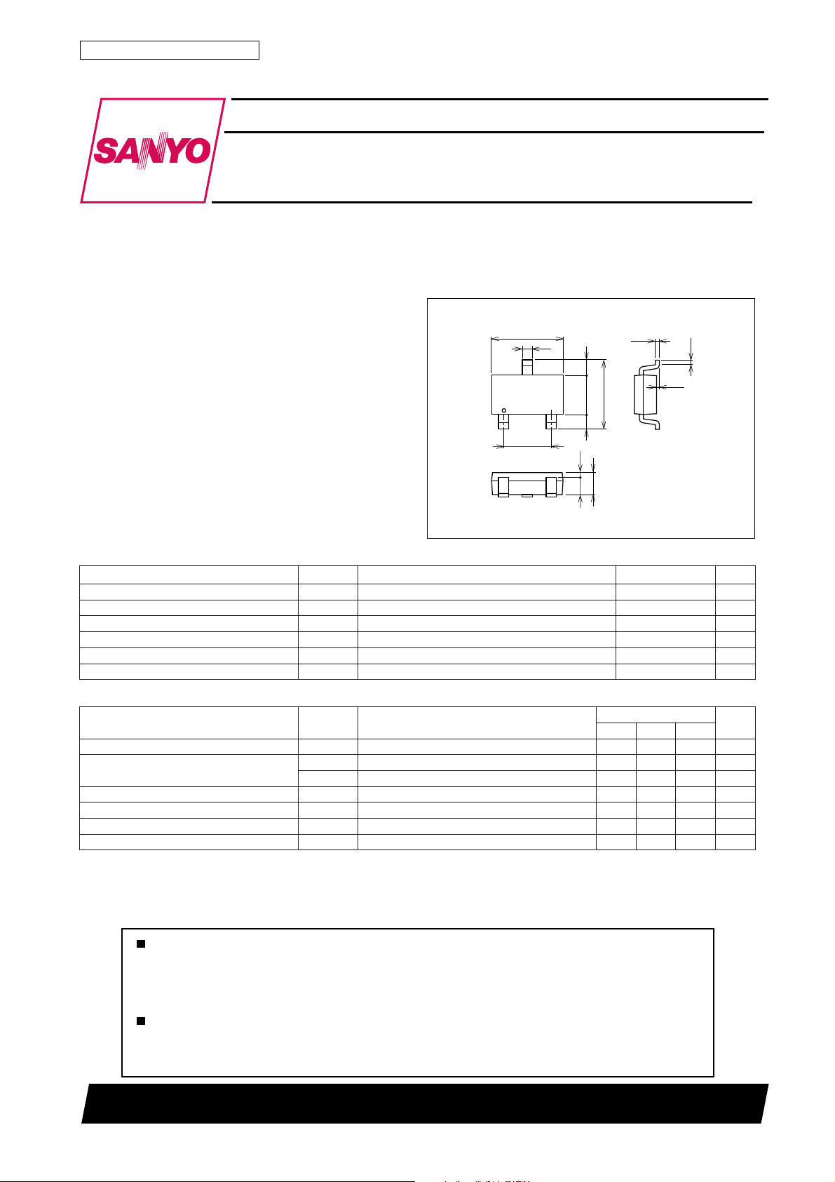
Package Dimensions
unit:mm
1293
[SBS004]
2.8
0.9
nimpytxam
0.15
0.05
1 : Anode
2 : No Contact
3 : Cathode
SANYO : CPH3
sgnitaR
0.2
51V
51V
1A
˚C
˚C
tinU
˚C/W
0.4
3
1.6 0.60.6
1
elcyc1,evaweniszH05 01A
IRAm1=51V
VRV6= 005Aµ
R
IFI=
R
Mounted on a ceramic board (600mm2×0.8mm)
zHM1=f,V01=24Fp
2
1.9
0.7 0.2
.tiucriCtseTdeificepseeS,Am001= 51sn
73099GI (KT) No.6272–1/3
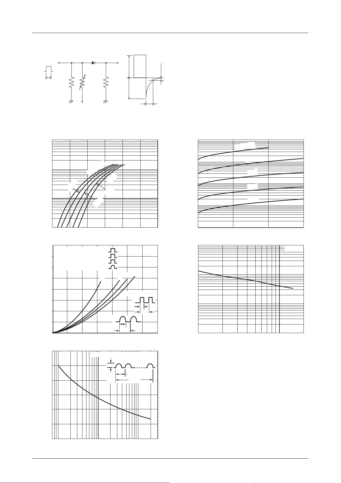
trr T est Circuit
Duty≤10%
SBS004
50Ω 100Ω 10Ω
10µs
10
7
5
3
2
-- A
1.0
F
7
5
3
2
0.1
7
Forward Current, I
5
3
2
0.01
0
0.8
-- W
0.7
(AV)
F
0.6
0.5
0.4
0.3
0.2
0.1
0
0
Average Forward Power Dissipation, P
100
⁄Rectangular wave θ=60°
¤Rectangular wave θ=120°
‹Rectangular wave θ=180°
›Sine wave θ=180°
0.2 0.4 0.6 0.8
Average Forward Current, I
12
-- A
10
(Peak)
8
FSM
6
--5V
I
F
Ta=125°C
°C
75°C
Forward Voltage, V
PF(AV) -- I
I
S
Current waveform 50Hz sine wave
-- V
F
25°C
50°C
0.3 0.4 0.50.1 0.2
⁄
Sine wave
-- t
Is
100mA100mA
-- V
F
O
›
‹
¤
Rectangular wave
180°
360°
1.0 1.2 1.4
-- A
O
20ms
t
θ
360°
trr
IT00622
IT00624
0.6
10mA
I
-- V
100
7
5
3
2
10
7
5
-- mA
3
R
2
1.0
7
5
3
2
0.1
Reverse Current, I
7
5
3
2
0.01
0
R
Ta=125
100
75°C
50°C
25°C
°C
°C
Reverse Voltage, V
1000
7
5
3
-- pF
2
100
7
5
3
2
10
7
5
3
Interterminal Capacitance, C
2
1.0
1.0 10
2
C -- V
357 2
Reverse Voltage, V
R
15510
IT00623
R
-- V
R
f=1MHz
R
-- V
IT00625
4
2
Surge Forward Current , I
0
7
0.01
23 7
52 237
0.1
Time, t -- s
5
1.0
3
IT00626
No.6272–2/3
 Loading...