

Page 1
- 58 -
IC836 on the main board stores the data for the service
adjustments, and should not be replaced except for the
case of defective device.
If replaced, it should be performed the re-adjustments
following to the “Electrical Adjustments”.
The data of lamp replacement monitor timer is stored in
the IC836.
Please note that the lamp replace counter is reset
when the memory IC (IC836) is replaced.
(Lamp replace counter can not be set to the previous
value.)
● Caution to memory IC replacement
When IC836 is replaced with new one, the CPU writes
down the default data of the service adjustments to the
replaced IC, refer to the service adjustment table. As
these data are not the same data as factory shipped
data, it should be required to perform the re-adjustments following to the “Electrical Adjustments”.
Please note that in this case the lamp replace counter
will be reset.
● Caution of Main Board replacement (in the case
IC836 is not defective)
When the main board is replaced, IC836 should be
replaced with the one on previous main board. After
replacement, it should be required to perform the readjustments following to the “Electrical Adjustments”.
In this case, the lamp replace counter can be kept the
value as before.
● Memory IC Replacement
Contrast Adjustment
R-Contrast adjustment ●❍ ●
G-Contrast Adjustment ●❍ ●
B-Contrast adjustment ●❍ ●
Condenser lens adjustment ❍❍
Relay lens adjustment ❍❍
Picture image adjustment ❍❍ ●●
Picture focus adjustment ❍❍ ●●
Output voltage adjustment ❍
Fan minimum voltage adjustment ●
TV sound level adjustment ●
TV stereo separation adjustment ●
TV video level adjustment ●
Common center adjustment ●●
Panel luminance adjustment ❍❍
White balance adjustment ❍❍
Color shading correction ❍❍
● : Adjustment necessary ❍ : Check necessary
Disassembly / Replaced Parts
LCD/
Prism
unit
Opti-
cal
unit
Polarized glass
RGB
Optical Adjustments
Electrical Adjustments
Main
Board
Screen
and
mirror
Powe r
Board
Digital
Board
Projec
-tion
lens
After replacing electrical parts and optical parts, electrical adjustments and optical adjustments are required.
■ Adjustments after Parts Replacement
Page 2
- 59 -
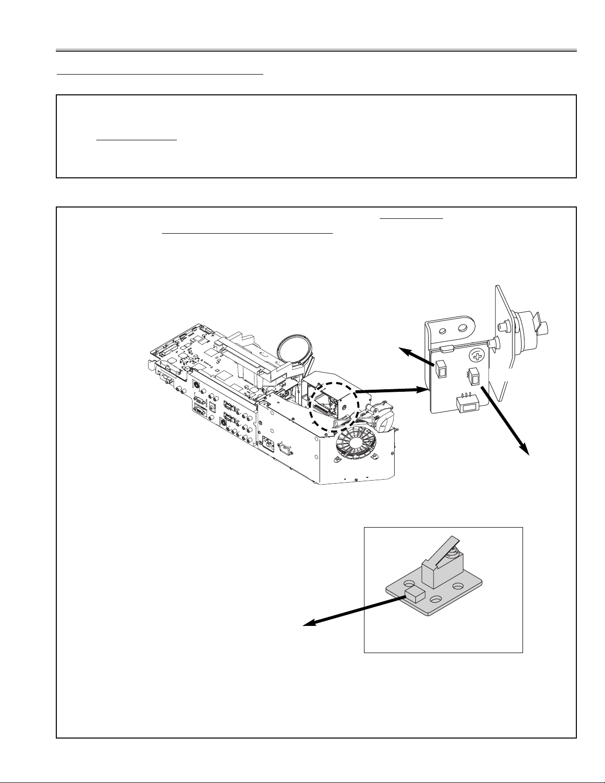
Note: The connector K18U is for the lamp cover switch, so you should short SW1861 on the Cover SW board.
Or you should short between 1 pin and 3 pin of K18U.
Before taking optical adjustments, remove the optical / chassis unit, front panel unit, key unit, digital unit following to
the “Mechanical Disassemblies”
Note: Do not disconnect connectors on the main board, except for K01L, K01R, K35R, K35G, or K35B, because
the LCD Projection TV can not be turned on due to operate the power failure protection.
OPTICAL / CHASSIS UNIT
● Preparation for Adjustments
LAMP COVER SWITCH
(SW1861)
Joint Board " K18U
Joint Board
Main Board " K8S "
Cover SW Board
Cover SW Board " K18S "
K18U
■ Optical Adjustments
Page 3
- 60 -
Optical adjustments
Note:
If the picture is left / right reversed on a screen, you can
select front or rear projection for your convenience.
Rear function
1. Enter the service mode.
2. Select item no. "400" and change data value to select
a direction of projection.
Item no. Adjustment value Function
400 0 Front projection
1 Rear projection
3. Exit the service mode.
---
4. After servicing, this item should be set to default
value = 1.
Note: Service mode is refer to "Service Adjustment
Menu Operation".
Front function
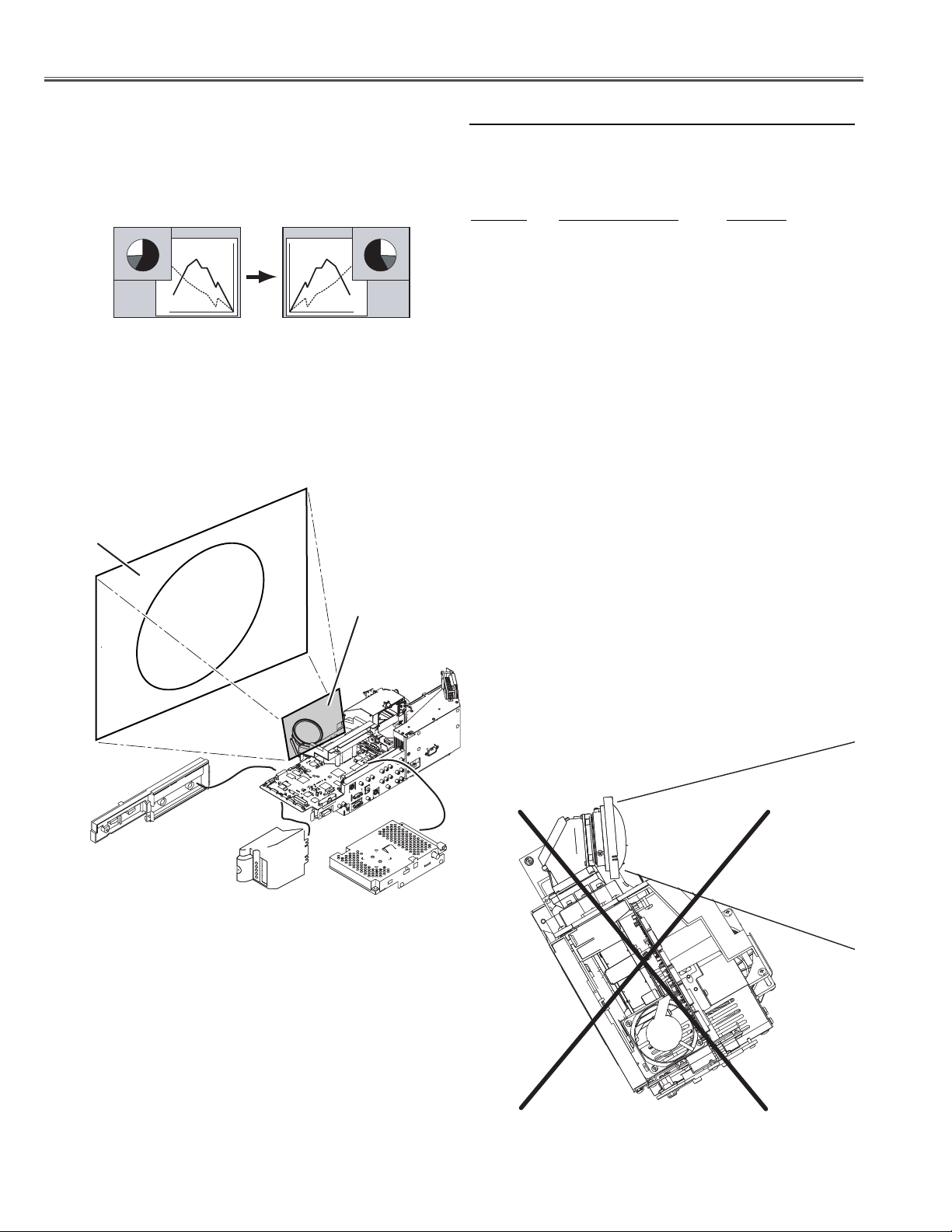
Overview for Servicing (an example)
● Rear - Front Project SW
Warning!
Do not use Optical/chassis unit with inclining.
It may result in malfunction of the LCD Projection TV
Screen
Mirror
Page 4
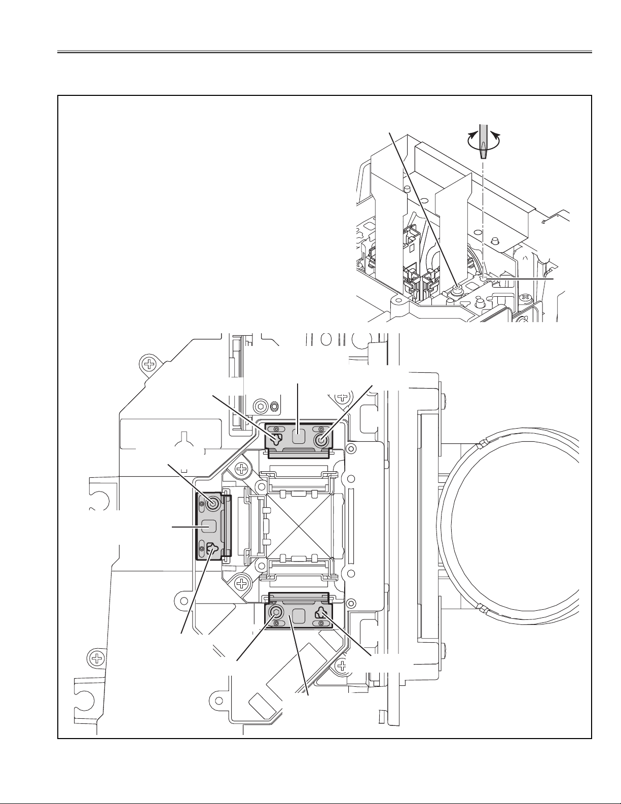
- 61 -
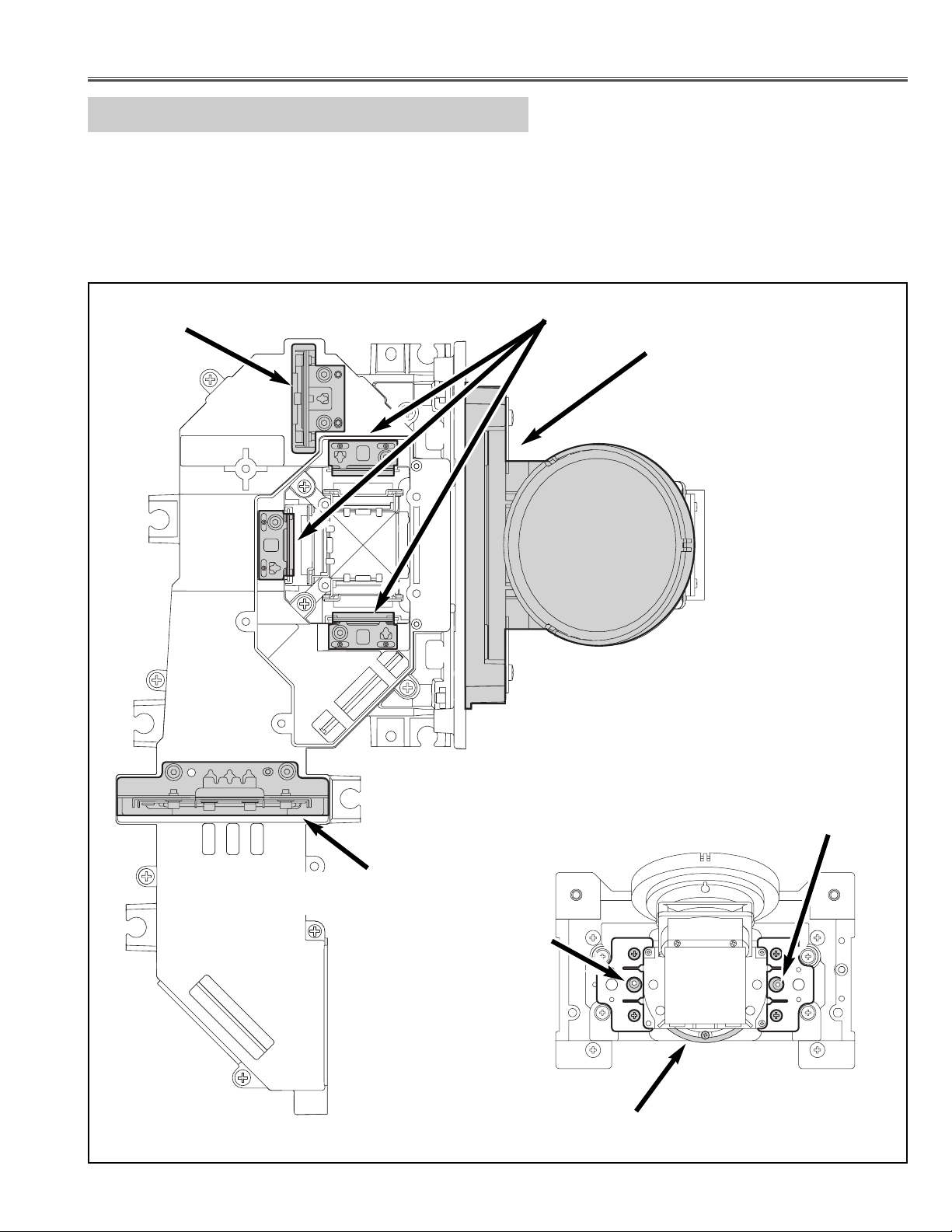
Optical adjustments
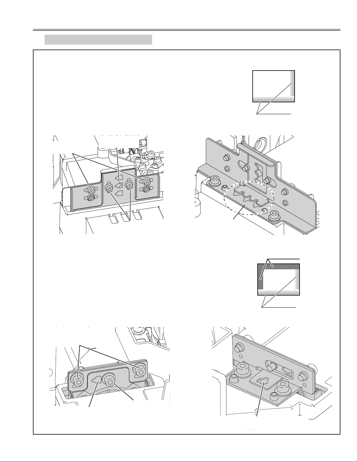
Adjustment of optical components location
Blue mirror, Condenser lens, Relay lens and contrast adjustment operate it from a back side.(Item1-1~1-3)
(Remove the Optical/Chassis unit from the Cabinet)
Picture image and focus adjustment operate it from a front side.(Item 2-1~2-3)
(An optical unit must be fixed.)
(Install the cabinet bottom cover.)
Projection lens
FRONT VIEW
(2-2) Vertical centering
adjustment
(2-1) Horizontal centering
adjustment
(2-3) Picture focus adjustment
Picture image and focus
adjustment
(1-3) Contrast adjustment
(1-1) Relay lens adjustment
(b)
(a),(c)
(1-2) Condenser lens
adjustment
Page 5

- 62 -
Optical adjustments
Optical components adjustments procedure
When adjusting optical components, adjust each adjustment item in numerical order.
Incorrect adjustment steps may produce improper adjustment. The items adjusted correctly can
be omitted from the steps.
Pre-adjustment
(a) Condenser lens setting
(b) Relay lens adjustment
(c) Condenser lens adjustment
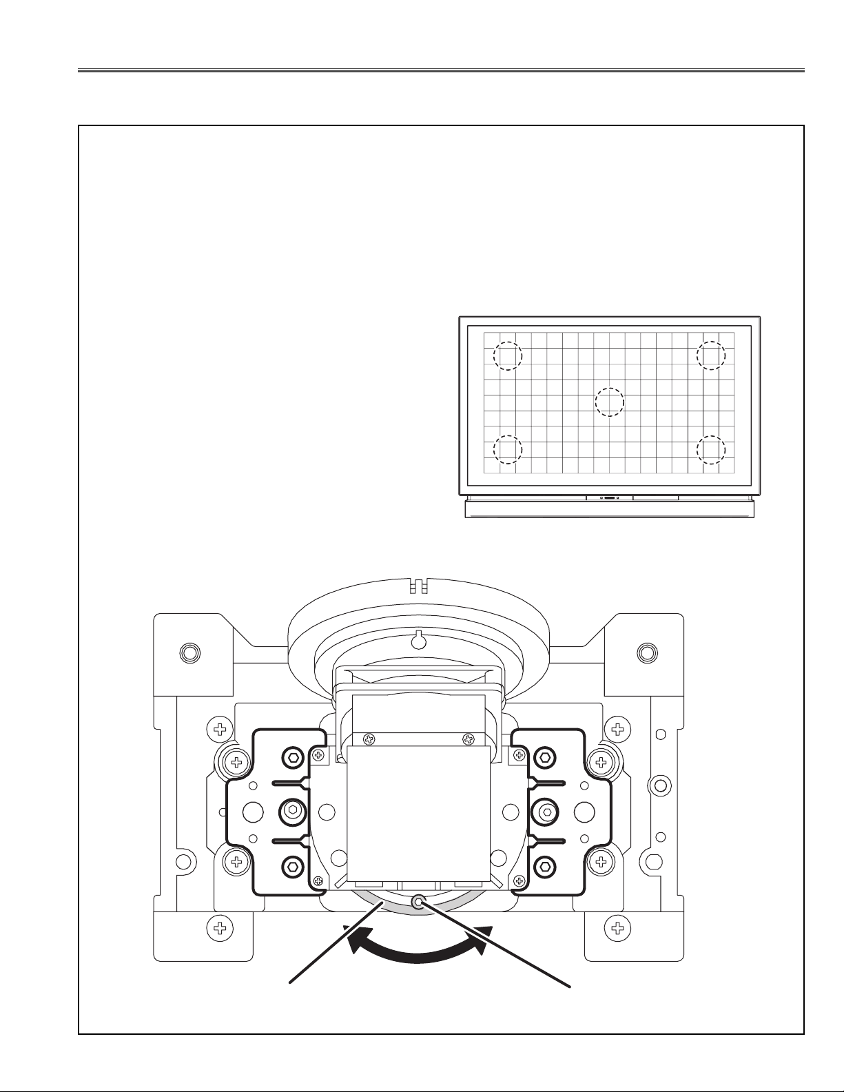
1. Optical system adjustment (Optical axis adjustment)
(1-1) Relay lens adjustment
(1-2) Condenser lens adjustment
(1-3) Contrast adjustment (Polarized glass adjustment) R,G,B
2. Picture image and focus adjustment
(2-1) Horizontal centering adjustment
(2-2) Vertical centering adjustment
(2-3) Picture focus adjustment
When the Optical unit is disassembled, the pre-adjustment is necessary.
The pre-adjustment can be omitted usually.
Page 6
- 63 -
Optical adjustments
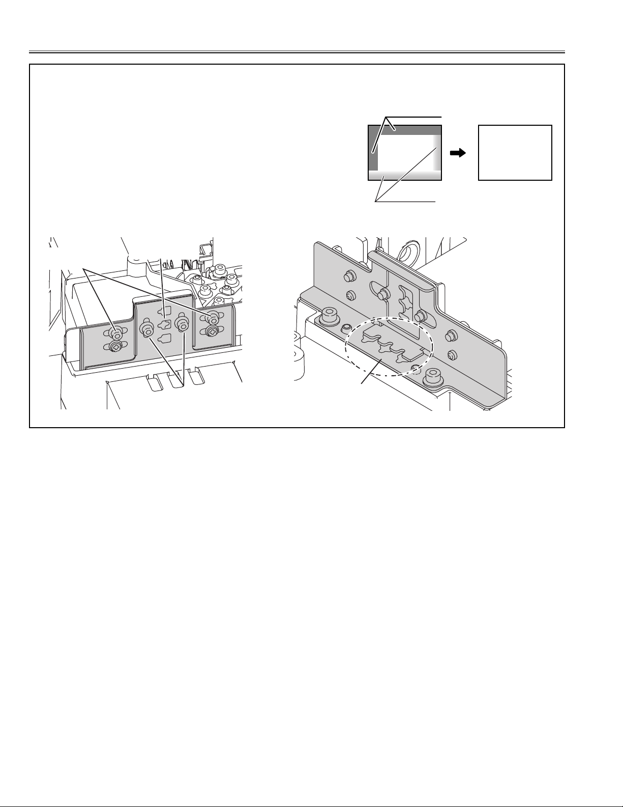
(b) Relay lens pre-adjustment
Loosen the 2 screws I and screw K.
Adjust the slot J to make shading(Cyan) appears on the right of the
screen as shown in figure. (The same amount as red is appeared on
the other side.)
Adjust the slot L to make shading(Cyan) appears on the bottom of the
screen as shown in figure. (The same amount as red is appeared on
the other side.)
Tighten 2 screws I and screw K.
Optical Pre-adjustment
Tu rn the LCD projection TV on by a state of without FPC cables.
(a) Condenser lens pre-adjustment
Loosen the 2 screws A and 2 screws C.
Adjust the slot B to make shading(Red) appears on the right of the
screen as shown in figure.
Adjust the slot D to make shading(Red) appears on the bottom of the
screen as shown in figure.
(The screws are tightened later. The screws are tightened in step-d)
White
Shade (Red)
Screw A
Slot D
Screw C
Slot B
Shade (Cyan)
White
Shade (Red)
Screw I
Slot J
Screw K
Slot L
Page 7
- 64 -
Optical adjustments
(c) Condenser lens pre-adjustment
Adjust the slot B to make color uniformity in white.
(Shading disappears on the right of the screen. Red and Cyan)
Adjust the slot D to make color uniformity in white.
(Shading disappears on the bottom of the screen. Red and Cyan)
Tighten 2 screws A and 2 screws C.
Shade (Cyan)
White
White
Slot D
Screw A
Screw C
Shade (Red)
Slot B
Page 8
- 65 -
Optical adjustments
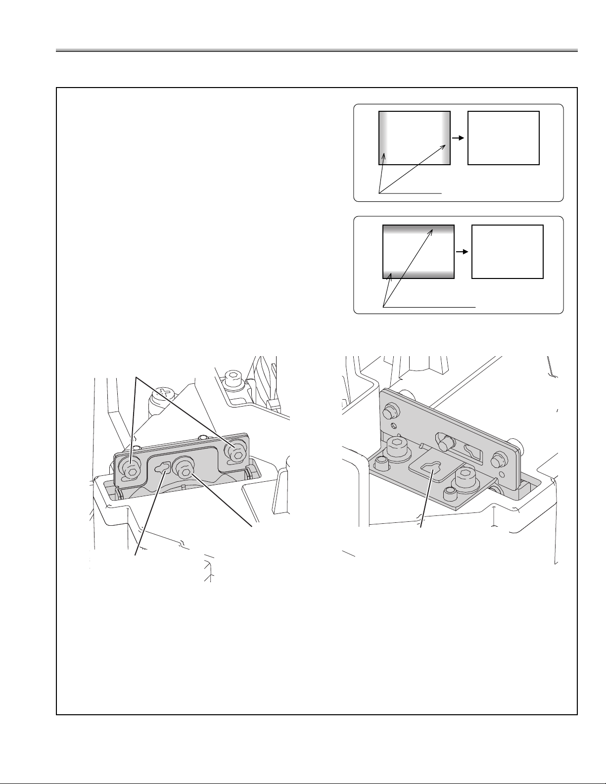
1-1. Relay lens adjustment
1. Turn the LCD projection TV on by a state of without FPC
cables.
2. Adjust the adjustment base of Relay lens unit to make
color uniformity in white.
a) If the shading appears on the left or right of the screen
as shown in figure, loosen 2 screws A with the ball allen
wrench, and adjust the slot B to make color uniformity in
white by using a slot screwdriver.
b) If the shading appears on the top or bottom of the
screen as shown in figure, loosen screw C with the ball
allen wrench, and adjust the slot D to make color uniformity
in white by using a slot screwdriver.
3. Tighten 2 screws A and screw C to fix the condenser lens
unit.
Shade
White
White
Shade
White
White
Screw A
Slot D
Screw C
Slot D
Page 9
- 66 -
Optical adjustments
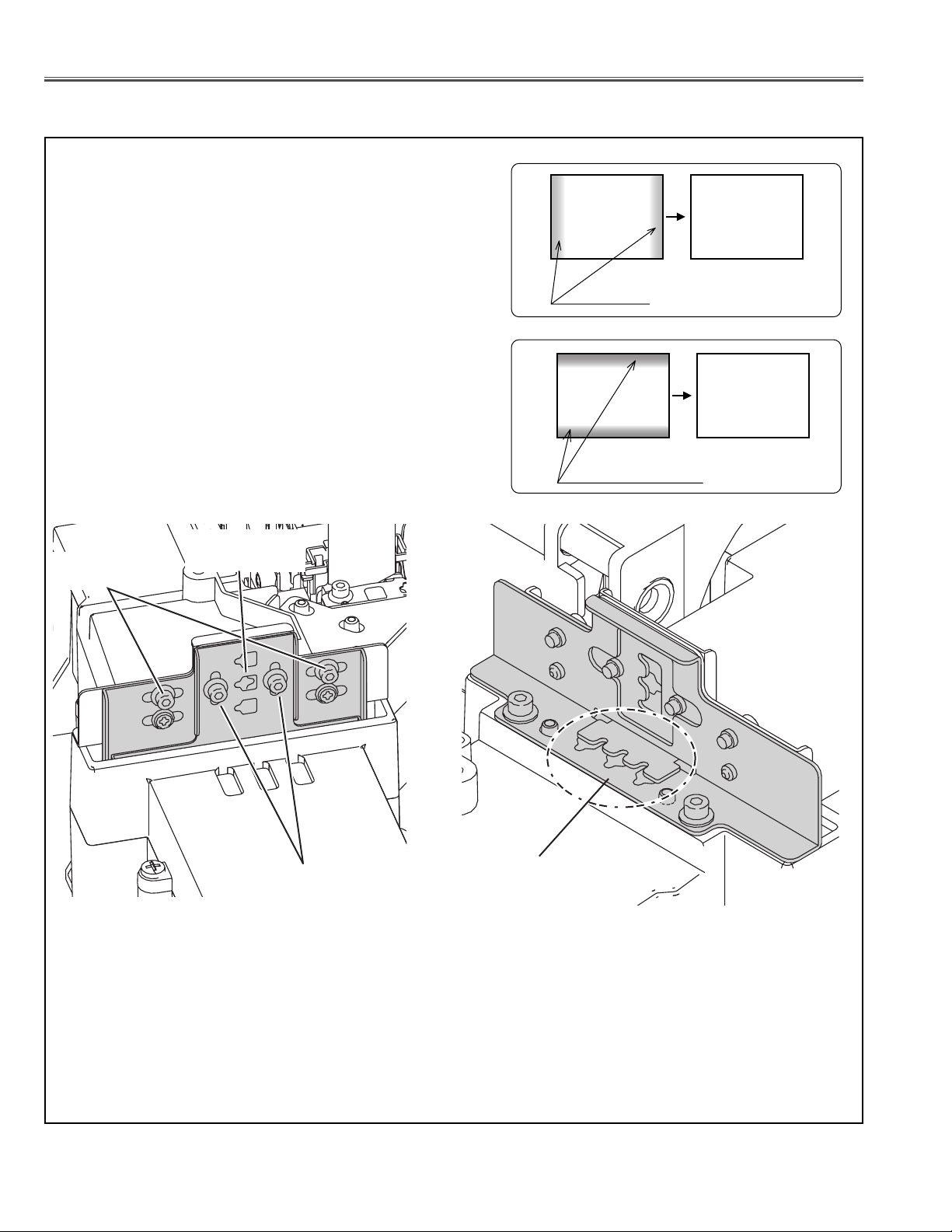
1-2. Condenser lens adjustment
1. Turn the LCD projection TV on by a state of without FPC
cables.
2. Adjust the adjustment base of Condenser lens unit to make
color uniformity in white.
a) If the shading appears on the left or right of the screen
as shown in figure, loosen 2 screws A with the ball allen
wrench, and adjust the slot B to make color uniformity in
white by using a slot screwdriver.
b) If the shading appears on the top or bottom of the
screen as shown in figure, loosen 2 screws C with the
ball allen wrench, and adjust the slot D to make color unifor-
mity in white by using a slot screwdriver.
3. Tighten 2 screws A and 2 screws C to fix the condenser
lens unit.
Shade
White
White
Shade
White
White
Screw A
Slot D
Screw C
Slot B
Page 10
- 67 -
Optical adjustments
1-3. Contrast adjustment (R,G,B, polarized glass)
Screw-A
Slot-B
R, G and B Contrast adjustment :
1. Tu rn the LCD projection TV on and input a 100% of black raster
signal (0% of white raster signal).
2. Loosen screw A on the polarizer unit which you intend to adjust
using ball allen wrench.
3. Turn the polarized glass mounting base (slot B) by using a slot
screwdriver and adjust the brightness on the screen to the low-
est level of black.
4. Tighten the screw A to fix the polarizer unit.
5. Adjust the polarizer unit of other colors.
(Repeat steps 2 to 4.)
R-Polarized glass
mounting base
Slot B
Screw-A
Slot-B
Screw A
Screw A
G-Polarized glass
mounting base
Slot B
Screw A
Slot B
B-Polarized glass
mounting base
Page 11
- 68 -
Optical adjustments
2
Picture Image and focus adjustment (Projection lens adjustment)
Screw-A
Focus ring-E
Adjustment Cam-B
Adjustment Cam-C
Screw-D
Screw-A
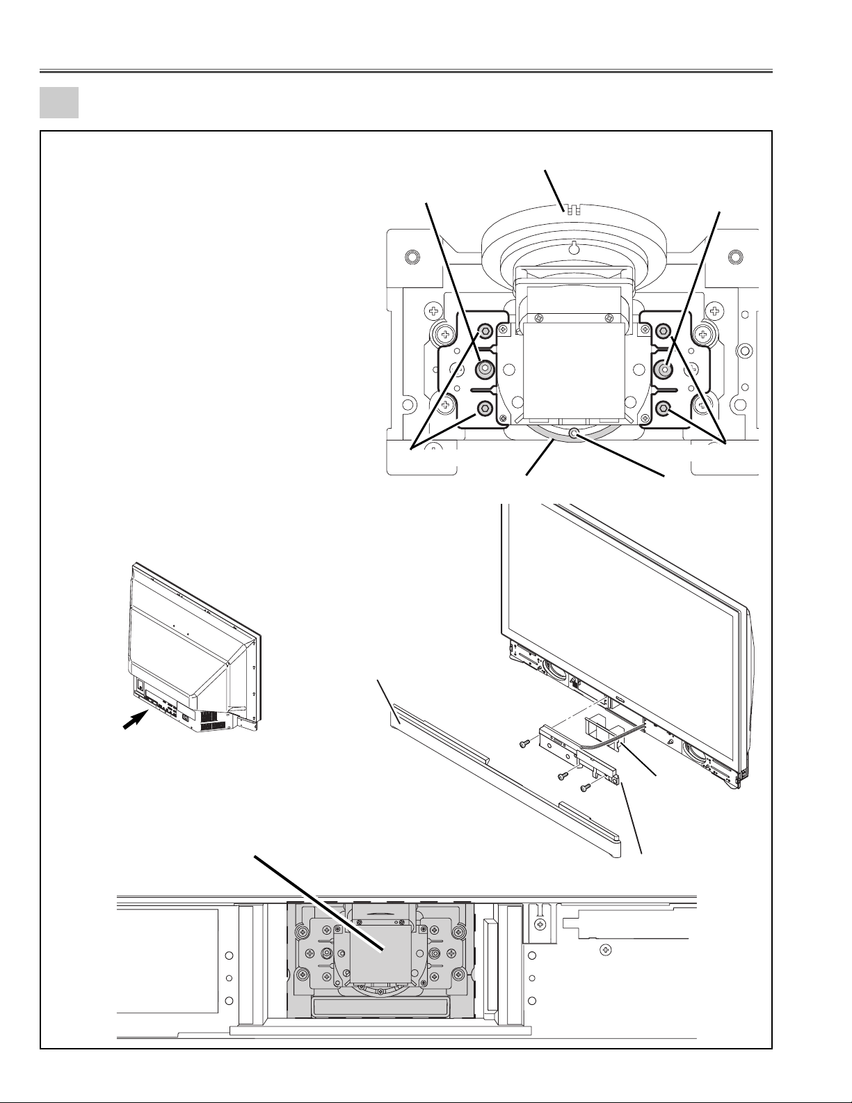
Projection lens
Remove the Front cover unit, remove the Front
panel unit and remove the Optical cover.
Adjustment area
Install all parts on a back side.
Before adjustment
1. Turn the LCD projection TV on and display grid
pattern or circular pattern on the screen.
2. Be sure to fixed the Optical / Chassis unit with 3
screws to the cabinet.
Install all parts on a back side, otherwise it may
cause lose of performance of Optical
Adjustment.
(Refer to mechanical disassemblies.)
3. Remove the Front Cover unit from the cabinet
bottom.
4. Remove the 3 screws F and remove the Front
panel unit.
5. Remove the Optical Cover.
(Refer to mechanical disassemblies.)
6. When adjust the picture image (horizontal centering and vertical centering) , loosen the 4 screws
A of the lens shift unit.
7. When adjust the picture focus, loosen the focus
fixed screw D of the projection lens.
Front cover
F
F
F
Optical cover
Front panel
Page 12
- 69 -
Optical adjustments
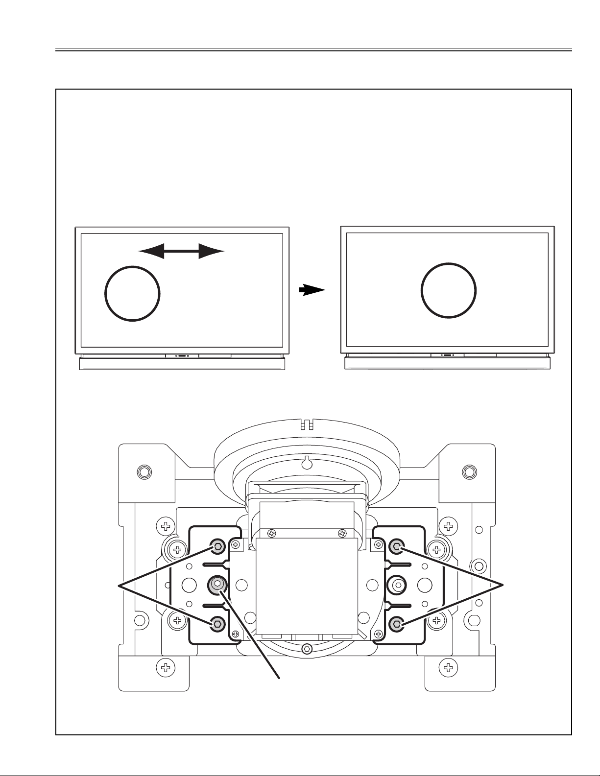
2-1. Horizontal centering adjustment
When the picture is shifted to right or left, adjust the picture horizontally.
1. Loosen the 4 screws A from the lens shift unit.
2. Project the circular pattern on screen.
3. Turn the adjustment cam B to right or left and adjust the position to
project the picture on just center of the screen.
4. Tighten the 4 screws A.
Picture image movement
Horizontal centering
Screw-A
Screw-A
Adjustment cam-B
Page 13
- 70 -
Optical adjustments
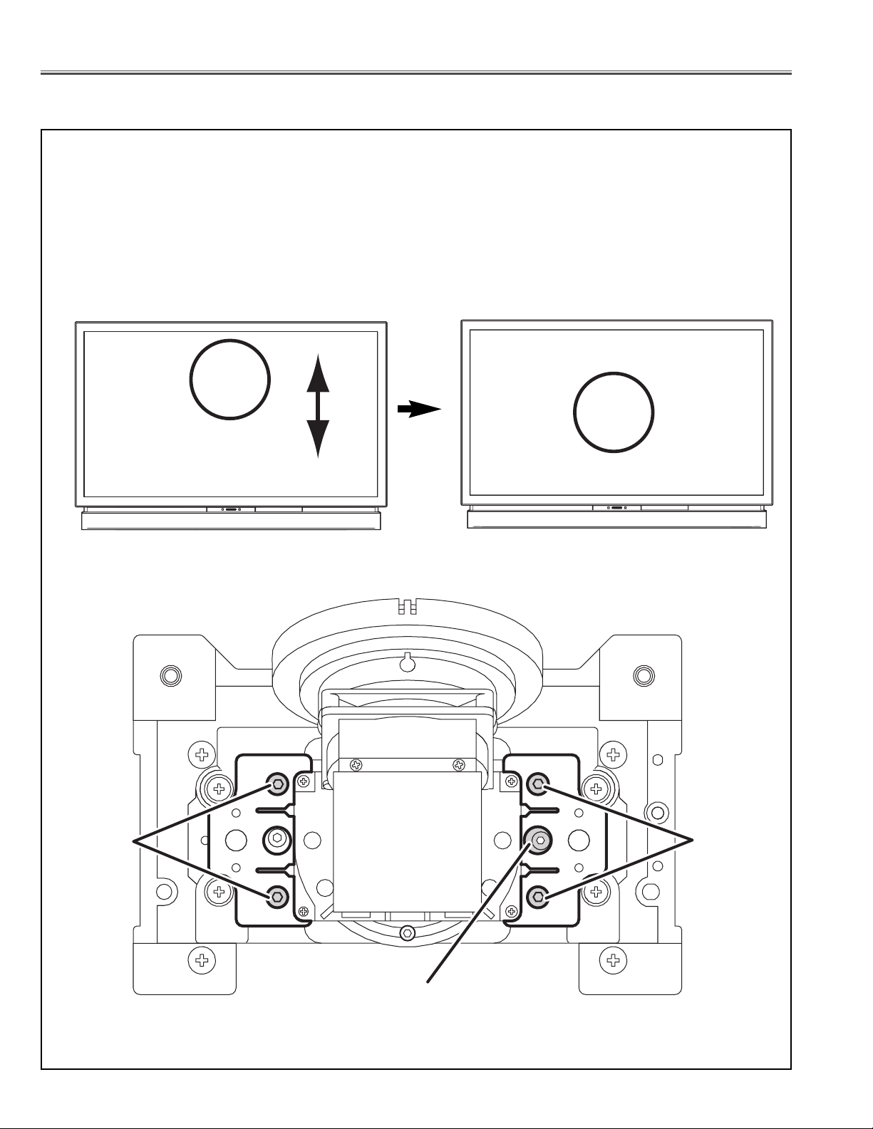
2-2. Vertical centering adjustment
When the picture is shifted to right or left, adjust the picture vertically.
1. Loosen the 4 screws A from the lens shift unit.
2. Project the circular pattern on screen.
3. Turn the adjustment cam C to right or left and adjust the position to
project the picture on just center of the screen.
4. Tighten the 4 screws A.
Picture image movement Vertical centering
Screw-A
Screw-A
Adjustment cam-C
Page 14
- 71 -
Optical adjustments
2-3. Picture focus adjustment
When the picture is off focused, adjust the picture focus.
1. Loosen the Projection lens focus lock screw D and turn the focus ring
E for best focus.
Be sure to tighten the Projection lens focus lock screw D and fix the
Projection lens after adjustment.
Adjust center part and four corners on
the grid pattern to sharp focus.
1
4
5
2
3
Focus ring-E
Turn the Focus ring-E
Focus lock screw-D
Page 15
-72-
● Service Adjustment Menu Operation
Remote Control
Side Control
◆ To enter service mode
To enter service mode, press and hold the "INFO" button on the remote control, then press the "VOL(–)" button on the side control. As shown in a figure,
the service mode display appears on the screen.
◆ To adjust service data
Adjust service data using the following control buttons on the LCD projection
TV or the remote control.
– "CHANNEL UP" ..........................................An item number increases.
– "CHANNEL DOWN" ..................................An item number decreases.
– "POINT RIGHT" or "VOLUME (+)" ............An adjustment value increases.
– "POINT LEFT" or "VOLUME (–)" ..............An adjustment value decreases.
◆ To exit service mode
To quit the service mode, press the "POWER ON/OFF" button only once on
the LCD projection TV or the remote control.
Data value
Item No.
Temperature
Fan rotation speed
Note :
This part of display is available at the service mode No.600s.
■ Electrical Adjustments
w
q
e
VOL(-)
Normal Mode
+
INFO
Service Mode
Service Mode
INPUT
VOLUME
CHANNEL
VOL(-)
w
INFO
q
POWER
e
Service Mode Display
NO 0 Data 105
TA TB TC
2662 3237 3050
F1 F2 F3 F4
80 100 100 100
Page 16

-73-
● Circuit Adjustments
CAUTION: The each circuit has been made by the fine adjustment at factory. Do not attempt to adjust the follow-
ing adjustments except requiring the readjustments in servicing otherwise it may cause loss of performance and product safety.
Note: Please refer to “Service Adjustment Menu Operation” for entering to the service mode and adjusting
the service data.
Equipment Digital voltmeter
1. Enter the service mode.
2. Change data values of each test points to adjust the
fan minimum output voltage.
Item no
. Fan Location Test Point Adjustment value
0 FN905/6 TPFAN1 8.0 ±0.05Vdc
1 FN901 TPFAN2 8.0 ±0.05Vdc
2 FN903/4 TPFAN3 8.0 ±0.05Vdc
3 FN902 TPFAN4 8.0 ±0.05Vdc
Note:
The location of each fan is refer to P.90.
x Fan minimum voltage adjustment
Equipment Digital voltmeter
1. Adjust the voltage by using VR621 on the power
board as following.
Test Point AC Input Reading
(+) 1pin of K6A 120V . . . . . .355V ±2Vdc
(–) 3pin of K6A (or 230V . . . . .370V ±2Vdc)
Caution:
Be sure to connect the lamp when taking this adjustment.
"K6A" is in the primary circuit. HO
T CIRCUIT!
Note:
The Power Board for replacing is already adjusted in a
factory, so it is not required to perform this readjustment.
z Output voltage adjustment
Electrical Adjustments
[Adjustment Condition]
● Input signal
Video signal .......................... 1.0Vp-p/75Ω terminated, color bar pat-
tern, 16 steps gray scale pattern, and
100%/50% white pattern (Composite
video signal)
Component video signal ...... 0.7Vp-p/75Ω terminated, color bar pat-
tern (480i format)
RF Audio signal .................... 1KHz 100% modulation signal and
multi stereo signal
● Picture setup menu .................. Before the electrical adjustments from step [ 6 ] to step [ 11 ], the picture
setup menu should be set as follows;
Main menu > Picture setup menu >
Picture --- Auto
16 steps gray scale pattern
White 100%
Black 100%
Page 17

-74-
Electrical Adjustments
Equipment Oscilloscope
Input mode Analog TV mode
Input signal Color bar pattern
1. Adjust the amplitude "a" by using VR101 on the
tuner board.
Test Point
Adjustment value
(+) TPTV 1.0 ±0.03Vdc
(–) TUNER_GND
b TV video level adjustment
Equipment Oscilloscope
Input mode Analog TV mode
Audio mode Stereo mode
Input audio signal Multi sound program
1. Enter the service mode.
2. Adjust the amplitude of 4KHz at Audio output-(L) terminal to become minimum level.
Item no. Test Point Adjustment value
751 (+) L audio output Minimum at 4KHz
(–) GND
3. Adjust the amplitude of 300Hz at Audio output-(R)
terminal to become minimum level.
Item no. Test Point Adjustment value
752 (+) R audio output Minimum at 300Hz
(–) GND
v TV stereo separation adjustment
Equipment Digital voltmeter
Input mode Analog TV mode
Input audio signal 1KHz 100% modulation
1. Enter the service mode.
2. Adjust the audio output amplitude at Audio output-(L)
terminal to become 400 ±10 mVac.
Item no. T
est Point Adjustment value
750 (+) L audio output 500 ±10 mVac
(–) GND
Note:
At the case with using an oscilloscope, adjust the
audio output amplitude at Audio output-(L) terminal to
become 1.41 ±0.02 Vp-p.
c TV sound level adjustment
(a)
Minimum leakage
4KHz
Minimum leakage
300Hz
Page 18

-75-
Electrical Adjustments
Input mode Not designated
Input signal 50% whole green, blue or red signal
Picture Auto
Lamp mode High
1. Enter the service mode.
2. Select item no. "308", and change data value from
"0" to "2". (Flicker adjustment mode ...see Note)
3. Receive 50% whole green, blue or red signal and project only one color component to the screen.
4. Change data value to obtain the minimum flicker for
each color on the screen.
5. After this adjustment, select item no. "308", and
change data value from "2" to "0" for normal operation. (Or turn off the projection TV, then this data value
will be reset to "0".)
Item no. Screen
4 Only green color picture
5 Only blue color picture
6 Only red color picture
Note:
The FRP signal (common electrode reverse signal)
works at 120Hz, so flicker is invisible for human eyes.
The service mode no. "308" can change the FRP signal from 120Hz to 60Hz, and flicker can be seen.
n Common center adjustment
Input signal 16-step gray scale signal
Input mode VIDEO_1 [Video] mode
Picture Auto
Lamp mode High
1. Enter the service mode.
2. Select group/item no. “8”(Blue) or “9”(Red), and
change data values respectively to make a proper
white balance.
Note:
If the luminance meter is not equipped, you can take
another method instead as follows;
1. When the main board is replaced, the data value at
"7/8/9" of the previous main board should be copied
manually.
2. If the main board is not replaced, you need not readjust these items.
, White balance adjustment [High]
Equipment luminance meter
Input mode VIDEO_1 [Video] mode
Picture Auto
Lamp mode High
1. Receive the 100% whole-white signal.
2. Enter the service mode.
3. Measure luminance on the screen with the luminance
meter. It is A for the reading of luminance meter.
4. Change the signal source to the 50% whole-white
signal.
5. Select item no. “7” and change data value to make the
reading of luminance meter to be A x 22±1%.
Item no. Screen Ajustment value
100% white A (reading value)
7 50% white A x 22 ±1%
m Panel luminance adjustment [High]
Page 19

-76-
Electrical Adjustments
If you find the color shading on the screen, please adjust
the white uniformity by using the proper computer and
“Color Shading Correction” software supplied separately. The software can be ordered as follows;
COLOR SHADING CORRECTION ver.. 4.00
Service Parts No. 645 075 9611
Note on WHITE UNIFORMITY Adjustment
Input mode VIDEO_1 [Video] mode
Picture Auto
Lamp mode Mid
1. Enter the service mode.
2. Receive the 100% whole-white signal.
3. Select item no. “13”(Green), “14”(Blue) or “15”
(Red), and change data values respectively to make
a proper white balance.
4. Receive the 50% whole-white signal.
5. Select item no. “17”(Blue) or “18”(Red), and change
data values respectively to make a proper white balance.
Note:
Confirm that the same white balance is obtained in
100% white and 50% white signals.
⁄0 White balance adjustment [Mid]
Equipment luminance meter
Input mode VIDEO_1 [Video] mode
Picture Auto
Lamp mode Mid
1. Enter the service mode.
2. Receive the 100% whole-white signal, and select
item no. “10”, the screen image will be whole-green.
3. Measure luminance on the screen with the luminance
meter. It is B for the reading of luminance meter.
4. Change the signal source to the 50% whole-white
signal.
5. Change data value to make the reading of luminance
meter to be B x 22±1%.
6. Receive the 100% whole-white signal, and select
item no. “11”, the screen image will be whole-blue.
7. Measure luminance on the screen with the luminance
meter. It is C for the reading of luminance meter.
8. Change the signal source to the 50% whole-white
signal.
9. Change data value to make the reading of luminance
meter to be C x 22±1%.
10. Receive the 100% whole-white signal, and select
item no. “12”, the screen image will be whole-red.
11. Measure luminance on the screen with the luminance meter. It is D for the reading of luminance
meter.
12. Change the signal source to the 50% whole-white
signal.
13. Change data value to make the reading of luminance meter to be D x 22±1%.
Item no. Screen Ajustment value
10 100% green B (reading value)
50% green B x 22±1%
11 100% blue C (reading value)
50% blue C x 22±1%
12 100% red D (reading value)
50% red D x 22±1%
Note:
If the luminance meter is not equipped, you can take
another method instead as follows;
1. When the main board is replaced, the data value at
"10/11/12" of the previous main board should be
copied manually.
2. If the main board is not replaced, you need not readjust these items.
. Panel luminance adjustment [Mid]
Page 20

FACTORY ADJUSTMENT
0Fan1 Min Adjust 0 ~ 255 105 ✻ FAN1 minimum voltage adjustment
1Fan2 Min Adjust 0 ~ 255 105 ✻ FAN2 minimum voltage adjustment
2Fan3 Min Adjust 0 ~ 255 105 ✻ FAN3 minimum voltage adjustment
3Fan4 Min Adjust 0 ~ 255 105 ✻ FAN4 minimum voltage adjustment
4 G_LCCOM 0 ~ 511 280 ✻ Common center adjustment [G]
5 B_LCCOM 0 ~ 511 280 ✻ Common center adjustment [B]
6 R_LCCOM 0 ~ 511 280 ✻ Common center adjustment [R]
7 G-GammaShift (Lamp mode=High) 0 ~ 1023 512 ✻ Panel luminance adjustment [High]
8 B-GammaShift(Lamp mode=High) 0 ~ 1023 512 ✻ White balance adjustment B [High]
9R-GammaShift (Lamp mode=High) 0 ~ 1023 512 ✻ White balance adjustment R [High]
10 G-GammaShift (Lamp mode=Mid or Low) 0 ~ 1023 512 ✻ Panel luminance adjustment G [Mid]
11 B-GammaShift (Lamp mode=Mid or Low) 0 ~ 1023 512 ✻ Panel luminance adjustment B [Mid]
12 R-GammaShift (Lamp mode=Mid or Low) 0 ~ 1023 512 ✻ Panel luminance adjustment R [Mid]
13 G-SubGain factor (Lamp=Mid or Low) 0 ~ 255 255 ✻ White balance adjustment 100% G [Mid]
14 B-SubGain factor (Lamp=Mid or Low) 0 ~ 255 255 ✻ White balance adjustment 100% B [Mid]
15 R-SubGain factor (Lamp=Mid or Low) 0 ~ 255 255 ✻ White balance adjustment 100% R [Mid]
16 G-GammaShift (Lamp mode=Mid or Low) 0 ~ 1023 512
17 B-GammaShift (Lamp mode=Mid or Low) 0 ~ 1023 512 ✻ White balance adjustment 50% B [Mid]
18 R-GammaShift (Lamp mode=Mid or Low) 0 ~ 1023 512 ✻ White balance adjustment 50% R [Mid]
19 G_V_CENTER 0 ~ 255 18
20 B_V_CENTER 0 ~ 255 18
21 R_V_CENTER 0 ~ 255 18
22 REF_G 0 ~ 255 191
23 REF_B 0 ~ 255 191
24 REF_R 0 ~ 255 191
25 GAIN_G (Lamp mode=Mid or Low) 360 ~ 535 512
26 GAIN_B (Lamp mode=Mid or Low) 360 ~ 535 512
27 GAIN_R (Lamp mode=Mid or Low) 360 ~ 535 512
PANEL DRIVER (L3E07110, L3E06150, L3E01060)
100 G-SubGain (Lamp mode=High) 360 ~ 535 512
101 B-SubGain (Lamp mode=High) 360 ~ 535 512
102 R-SubGain (Lamp mode=High) 360 ~ 535 512
103 G_OFFSET 0 ~ 255 0
104 B_OFFSET 0 ~ 255 0
105 R_OFFSET 0 ~ 255 0
106 G_ENBX1 ~ 4 Pulse Width 0 ~ 127 11
107 B_ENBX1 ~ 4 Pulse Width 0 ~ 127 11
108 R_ENBX1 ~ 4 Pulse Width 0 ~ 127 11
109 G_DXIN Delay 0 ~ 255 20
110 B_DXIN Delay 0 ~ 255 20
111 R_DXIN Delay 0 ~ 255 20
112 G_CLXIN Delay 0 ~ 255 20
113 B_CLXIN Delay 0 ~ 255 20
114 R_CLXIN Delay 0 ~ 255 20
115 G_ENBX Delay 0 ~ 255 14
116 B_ENBX Delay 0 ~ 255 14
117 R_ENBX Delay 0 ~ 255 14
118 G-SubBright 0 ~ 1023 0
119 B-SubBright 0 ~ 1023 0
120 R-SubBright 0 ~ 1023 0
121 G_ReferH (NRS Level) 0 ~ 1023 1020
122 B_ReferH (NRS Level) 0 ~ 1023 1020
123 R_ReferH (NRS Level) 0 ~ 1023 1020
124 G_ReferL (NRS Level) 0 ~ 1023 256
125 B_ReferL (NRS Level) 0 ~ 1023 256
126 R_ReferL (NRS Level) 0 ~ 1023 256
127 G V-Line Correction (-) Tilt 0 ~ 255 0
128 G V-Line Correction (-) 1 dot 0 ~ 511 503
129 G V-Line Correction (-) 2 dot 0 ~ 511 0
130 G V-Line Correction (-) 3 dot 0 ~ 511 0
-77-
● Service Adjustment Data Table
These initial values are the reference data written from the CPU
ROM to memory IC when replaced new memory IC. The adjustment items indicated with “✻” are required to readjust following
to the “Electrical adjustments”. Other items should be used with
the initial data value.
Electrical Adjustments
Item No. Adjustment Item Range Initial Value Description
Page 21

-78-
Electrical Adjustments
131 G V-Line Correction (-) 4 dot 0 ~ 511 0
132 G V-Line Correction (-) 5 dot 0 ~ 511 0
133 G V-Line Correction (-) 6 dot 0 ~ 511 0
134 G V-Line Correction (-) 7 dot 0 ~ 511 0
135 G V-Line Correction (-) 8 dot 0 ~ 511 0
136 G V-Line Correction (-) 9 dot 0 ~ 511 0
137 G V-Line Correction (-) 10 dot 0 ~ 511 0
138 G V-Line Correction (-) 11 dot 0 ~ 511 503
139 G V-Line Correction (-) 12 dot 0 ~ 511 503
140 B V-Line Correction (-) Tilt 0 ~ 255 0
141 B V-Line Correction (-) 1 dot 0 ~ 511 503
142 B V-Line Correction (-) 2 dot 0 ~ 511 0
143 B V-Line Correction (-) 3 dot 0 ~ 511 0
144 B V-Line Correction (-) 4 dot 0 ~ 511 0
145 B V-Line Correction (-) 5 dot 0 ~ 511 0
146 B V-Line Correction (-) 6 dot 0 ~ 511 0
147 B V-Line Correction (-) 7 dot 0 ~ 511 0
148 B V-Line Correction (-) 8 dot 0 ~ 511 0
149 B V-Line Correction (-) 9 dot 0 ~ 511 0
150 B V-Line Correction (-) 10 dot 0 ~ 511 0
151 B V-Line Correction (-) 11 dot 0 ~ 511 503
152 B V-Line Correction (-) 12 dot 0 ~ 511 503
153 R V-Line Correction (-) Tilt 0 ~ 255 0
154 R V-Line Correction (-) 1 dot 0 ~ 511 503
155 R V-Line Correction (-) 2 dot 0 ~ 511 0
156 R V-Line Correction (-) 3 dot 0 ~ 511 0
157 R V-Line Correction (-) 4 dot 0 ~ 511 0
158 R V-Line Correction (-) 5 dot 0 ~ 511 0
159 R V-Line Correction (-) 6 dot 0 ~ 511 0
160 R V-Line Correction (-) 7 dot 0 ~ 511 0
161 R V-Line Correction (-) 8 dot 0 ~ 511 0
162 R V-Line Correction (-) 9 dot 0 ~ 511 0
163 R V-Line Correction (-) 10 dot 0 ~ 511 0
164 R V-Line Correction (-) 11 dot 0 ~ 511 503
165 R V-Line Correction (-) 12 dot 0 ~ 511 503
166 G V-Line Correction (+) Tilt 0 ~ 255 0
167 G V-Line Correction (+) 1 dot 0 ~ 511 10
168 G V-Line Correction (+) 2 dot 0 ~ 511 0
169 G V-Line Correction (+) 3 dot 0 ~ 511 0
170 G V-Line Correction (+) 4 dot 0 ~ 511 0
171 G V-Line Correction (+) 5 dot 0 ~ 511 0
172 G V-Line Correction (+) 6 dot 0 ~ 511 0
173 G V-Line Correction (+) 7 dot 0 ~ 511 0
174 G V-Line Correction (+) 8 dot 0 ~ 511 0
175 G V-Line Correction (+) 9 dot 0 ~ 511 0
176 G V-Line Correction (+) 10 dot 0 ~ 511 0
177 G V-Line Correction (+) 11 dot 0 ~ 511 10
178 G V-Line Correction (+) 12 dot 0 ~ 511 10
179 B V-Line Correction (+) Tilt 0 ~ 255 0
180 B V-Line Correction (+) 1 dot 0 ~ 511 10
181 B V-Line Correction (+) 2 dot 0 ~ 511 5
182 B V-Line Correction (+) 3 dot 0 ~ 511 0
183 B V-Line Correction (+) 4 dot 0 ~ 511 0
184 B V-Line Correction (+) 5 dot 0 ~ 511 0
185 B V-Line Correction (+) 6 dot 0 ~ 511 0
186 B V-Line Correction (+) 7 dot 0 ~ 511 0
187 B V-Line Correction (+) 8 dot 0 ~ 511 0
188 B V-Line Correction (+) 9 dot 0 ~ 511 0
189 B V-Line Correction (+) 10 dot 0 ~ 511 0
190 B V-Line Correction (+) 11 dot 0 ~ 511 10
191 B V-Line Correction (+) 12 dot 0 ~ 511 10
192 R V-Line Correction (+) Tilt 0 ~ 255 0
193 R V-Line Correction (+) 1 dot 0 ~ 511 10
194 R V-Line Correction (+) 2 dot 0 ~ 511 5
195 R V-Line Correction (+) 3 dot 0 ~ 511 0
196 R V-Line Correction (+) 4 dot 0 ~ 511 0
197 R V-Line Correction (+) 5 dot 0 ~ 511 0
198 R V-Line Correction (+) 6 dot 0 ~ 511 0
Item No. Adjustment Item Range Initial Value Description
Page 22

Electrical Adjustments
-79-
199 R V-Line Correction (+) 7 dot 0 ~ 511 0
200 R V-Line Correction (+) 8 dot 0 ~ 511 0
201 R V-Line Correction (+) 9 dot 0 ~ 511 0
202 R V-Line Correction (+) 10 dot 0 ~ 511 0
203 R V-Line Correction (+) 11 dot 0 ~ 511 10
204 R V-Line Correction (+) 12 dot 0 ~ 511 10
205 DXOUTG 0 ~ 1023 214
206 DXOUTB 0 ~ 1023 214
207 DXOUTR 0 ~ 1023 214
208 h_change_pos 0 ~ 255 22
209 sh_base_pos_b 0 ~ 4096 2730
210 NRG Position 0 ~ 127 34
211 NRG Width 0 ~ 255 45
212 OSD 0 ~ 3 2
213 OSD 0 ~ 7 0
214 GAMMA (ON/OFF) 0-1 1
215 ref_gate_pos (NRS Position) 0 ~ 1023 1
216 ref_gate_dur (NR Width) 0 ~ 1023 157
217 gray_on 0 ~ 7 7
218 Correction 0 ~ 1 0
219 V Line Correction DC Offset EN 0 ~ 1 1
220 V Line Correction Offset EN 0 ~ 1 1
221 V Line Correction BLSP_EN 0 ~ 1 1
222 Sequential Ghost Correction EN 0 ~ 1 1
223 Block Ghost Correction EN 0 ~ 1 1
224 Reversal Ghost Correction EN 0 ~ 1 1
225 Rear Crosstalk Correction EN 0 ~ 1 1
226 G_base_pos 0 ~ 15 6
227 B_base_pos 0 ~ 15 6
228 R_base_pos 0 ~ 15 6
229 RGB_adjust 0 ~ 7 0
230 RGB_level 0 ~ 1023 0 5 Step Setting [0,256,512,768,1023]
231 V Line Correction <G0> 0 ~ 255 8
232 V Line Correction <G1> 0 ~ 255 6
233 V Line Correction <G2> 0 ~ 255 2
234 V Line Correction <G3> 0 ~ 255 254
235 V Line Correction <G4> 0 ~ 255 253
236 V Line Correction <B0> 0 ~ 255 8
237 V Line Correction <B1> 0 ~ 255 6
238 V Line Correction <B2> 0 ~ 255 2
239 V Line Correction <B3> 0 ~ 255 254
240 V Line Correction <B4> 0 ~ 255 253
241 V Line Correction <R0> 0 ~ 255 8
242 V Line Correction <R1> 0 ~ 255 6
243 V Line Correction <R2> 0 ~ 255 2
244 V Line Correction <R3> 0 ~ 255 254
245 V Line Correction <R4> 0 ~ 255 253
246 Ghost_G_pos (Sequential) 0 ~ 15 6
247 Ghost_B_pos (Sequential) 0 ~ 15 6
248 Ghost_R_pos (Sequential) 0 ~ 15 6
249 Ghost_G_center 0 ~ 2047 0
250 Ghost_G_start 0 ~ 255 128
251 Ghost_G_end 0 ~ 255 128
252 Ghost_B_center 0 ~ 2047 0
253 Ghost_B_start 0 ~ 255 128
254 Ghost_B_end 0 ~ 255 128
255 Ghost_R_center 0 ~ 2047 0
256 Ghost_R_start 0 ~ 255 128
257 Ghost_R_end 0 ~ 255 128
258 G-Block Ghost 0 ~ 2047 0
259 B-Block Ghost 0 ~ 2047 0
260 R-Block Ghost 0 ~ 2047 0
261 G_base_level (Block) 0 ~ 2047 0
262 B_base_level (Block) 0 ~ 2047 0
263 R_base_level (Block) 0 ~ 2047 0
264 Ghost_G_pos (Reverse) 0 ~ 2047 0
265 Ghost_B_pos (Reverse) 0 ~ 2047 0
266 Ghost_R_pos (Reverse) 0 ~ 2047 0
Item No. Adjustment Item Range Initial Value Description
Page 23

-80-
Electrical Adjustments
267 C_TALK G_CENT 0 ~ 2047 0
268 C_TALK G_START 0 ~ 255 128
269 C_TALK G_END 0 ~ 255 128
270 C_TALK B_CENT 0 ~ 2047 0
271 C_TALK B_START 0 ~ 255 128
272 C_TALK B_END 0 ~ 255 128
273 C_TALK R_CENT 0 ~ 2047 0
274 C_TALK R_START 0 ~ 255 128
275 C_TALK R_END 0 ~ 255 128
276 lccom_correct_select 0 ~ 1 0
277 iromura_correct_select 0 ~ 1 1
278 Hori Start 0 ~ 2047 266
279 Vert Start 0 ~ 2047 8
280 Hori End 0 ~ 2047 1545
281 Vert End 0 ~ 2047 728
282 G MIN 0 ~ 1023 594
283 G_MID2 0 ~ 1023 664
284 G_MID1 0 ~ 1023 736
285 G_MAX 0 ~ 1023 780
286 B MIN 0 ~ 1023 594
287 B_MID2 0 ~ 1023 664
288 B_MID1 0 ~ 1023 736
289 B_MAX 0 ~ 1023 780
290 R MIN 0 ~ 1023 594
291 R_MID2 0 ~ 1023 664
292 R_MID1 0 ~ 1023 736
293 R_MAX 0 ~ 1023 780
294 G MIN (8 Stair) 0 ~ 1023 705
295 G_MID2 (8 Stair) 0 ~ 1023 730
296 G_MID1 (8 Stair) 0 ~ 1023 757
297 G_MAX (8 Stair) 0 ~ 1023 787
298 B MIN (8 Stair) 0 ~ 1023 705
299 B_MID2 (8 Stair) 0 ~ 1023 730
300 B_MID1 (8 Stair) 0 ~ 1023 757
301 B_MAX (8 Stair) 0 ~ 1023 787
302 R MIN( (8 Stair) 0 ~ 1023 705
303 R_MID2 (8 Stair) 0 ~ 1023 730
304 R_MID1 (8 Stair) 0 ~ 1023 757
305 R_MAX (8 Stair) 0 ~ 1023 787
306 H_OUT_START 0 ~ 2047 102
307 Stair Output out of effective field 0 ~ 1023 0
308 Flicker Adjustment Mode 0 ~ 3 0 0: Off, 1: Flicker adj. mode 1, 2: Flicker adj. mode 2
309 Frame Modulation Step 0 ~ 3 2
310 H Crosstalk Correction 2 G center 0 ~ 2047 0
311 H Crosstalk Correction 2 G start 0 ~ 255 126
312 H Crosstalk Correction 2 G end 0 ~ 255 128
313 H Crosstalk Correction 2 B center 0 ~ 2047 0
314 H Crosstalk Correction 2 B start 0 ~ 255 126
315 H Crosstalk Correction 2 B end 0 ~ 255 128
316 H Crosstalk Correction 2 R center 0 ~ 2047 0
317 H Crosstalk Correction 2 R start 0 ~ 255 126
318 H Crosstalk Correction 2 R end 0 ~ 255 128
319 R_hosei point 0 0-3FF 0
320 R_hosei point 24 0-3FF 200
321 R_hosei point 48 0-3FF 420
322 R_hosei point 88 0-3FF 565
323 R_hosei point 140 0-3FF 615
324 R_hosei point 200 0-3FF 645
325 R_hosei point 300 0-3FF 685
326 R_hosei point 400 0-3FF 712
327 R_hosei point 500 0-3FF 738
328 R_hosei point 600 0-3FF 758
329 R_hosei point 700 0-3FF 782
330 R_hosei point 800 0-3FF 807
331 R_hosei point 900 0-3FF 841
332 R_hosei point 948 0-3FF 878
333 R_hosei point 980 0-3FF 950
334 R_hosei point 1024 0-3FF 1023
Item No. Adjustment Item Range Initial Value Description
Page 24

Electrical Adjustments
-81-
335 G_hosei point 0 0 ~ 3FF 0
336 G_hosei point 24 0 ~ 3FF 200
337 G_hosei point 48 0 ~ 3FF 420
338 G_hosei point 88 0 ~ 3FF 565
339 G_hosei point 140 0 ~ 3FF 615
340 G_hosei point 200 0 ~ 3FF 645
341 G_hosei point 300 0 ~ 3FF 685
342 G_hosei point 400 0 ~ 3FF 712
343 G_hosei point 500 0 ~ 3FF 738
344 G_hosei point 600 0 ~ 3FF 758
345 G_hosei point 700 0 ~ 3FF 782
346 G_hosei point 800 0 ~ 3FF 807
347 G_hosei point 900 0 ~ 3FF 841
348 G_hosei point 948 0 ~ 3FF 878
349 G_hosei point 980 0 ~ 3FF 950
350 G_hosei point 1024 0 ~ 3FF 1023
351 B_hosei point 0 0 ~ 3FF 0
352 B_hosei point 24 0 ~ 3FF 200
353 B_hosei point 48 0 ~ 3FF 420
354 B_hosei point 88 0 ~ 3FF 565
355 B_hosei point 140 0 ~ 3FF 615
356 B_hosei point 200 0 ~ 3FF 645
357 B_hosei point 300 0 ~ 3FF 685
358 B_hosei point 400 0 ~ 3FF 712
359 B_hosei point 500 0 ~ 3FF 738
360 B_hosei point 600 0 ~ 3FF 758
361 B_hosei point 700 0 ~ 3FF 782
362 B_hosei point 800 0 ~ 3FF 807
363 B_hosei point 900 0 ~ 3FF 841
364 B_hosei point 948 0 ~ 3FF 878
365 B_hosei point 980 0 ~ 3FF 950
366 B_hosei point 1024 0 ~ 3FF 1023
367 Color Shading Correction 4/8 Layer SW 3 3: 4 Layer, 7: 8 Layer
Option
400 Rear Projection On/Off 0 ~ 1 1 0: Front Projection, 1: Rear Projection
401 PANEL R/B Reversal 0 ~ 1 1 0: Normal, 1: Reverse (Bin - Rout, Rin - Bout)
402 OnTimer/OffTimer Flag 0 ~ 1 0 0: Normal, 1: Acceleration
LPS mode < 55 inch > < 65 inch >
500 LPS1_Wat 1 ~ 75 30 30
501 LPS2_Wat 1 ~ 75 30 30
502 LPS3_Wat 1 ~ 75 30 30
503 LPS1_Time 2 ~ 120 45 45
504 LPS2_Time 2 ~ 120 60 60
505 LPS3_Time 2 ~ 120 15 15
506 INITIAL_Time 0 ~ 255 120 120
507 INIT_CURRENT 20 ~ 80 75 75
508 STARTUP_TIME 2 ~ 10 6 6
509 PULSE_ON_OFF 0 ~ 1 1 1
510 PowerUP_Time 0 ~ 120 30 30
511 PowerUP_LEVEL 50 ~ 110 100 100
512 ECO_Power 50 ~ 100 77 77
513 START_Power 50 ~ 110 100 100
514 COLD Start Time 0 ~ 255 10 10
515 HOT Start Time 0 ~ 255 1 1
516 NORMAL_Power 50 ~ 110 94 94
Dimmer (Lamp Mode:Auto) < 55 inch > < 65 inch >
517 Not used - - -
518 Not used - - -
519 Not used - - -
520 Not used - - -
521 Not used - - -
522 Not used - - -
523 Not used - - -
524 Not used - - -
525 Not used - - -
526 Not used - - -
527 Not used - - -
528 Not used - - -
Item No. Adjustment Item Range Initial Value Description
Page 25

-82-
Electrical Adjustments
529 Not used - - -
530 Not used - - -
531 Not used - - -
532 Not used - - -
Fan Control
600 Fan1 Max Adjust 0 ~ 255 135
601 Fan2 Max Adjust 0 ~ 255 135
602 Fan3 Max Adjust 0 ~ 255 135
603 Fan4 Max Adjust 0 ~ 255 135
604 Fan Control Mode 0 ~ 1 0
605 Fan Max Min SW 0 ~ 3 0
< 55 inch > < 65 inch >
Normal Highland Normal Highland
606 Manual Fan1 Voltage 40 ~ 138 100 100 100 100
607 Manual Fan2 Voltage 40 ~ 138 100 100 100 100
608 Manual Fan3 Voltage 40 ~ 138 100 100 100 100
609 Manual Fan4 Voltage 40 ~ 138 100 100 100 100
610 Normal Fan1 Min 40 ~ 138 67 95 67 95
611 Normal Fan2 Min 40 ~ 138 73 90 73 90
612 Normal Fan3 Min 40 ~ 138 65 95 65 95
613 Normal Fan4 Min 40 ~ 138 80 90 80 90
614 Normal Fan1 Max 40 ~ 138 135 135 135 135
615 Normal Fan2 Max 40 ~ 138 95 116 95 116
616 Normal Fan3 Max 40 ~ 138 135 135 135 135
617 Normal Fan4 Max 40 ~ 138 135 135 135 135
618 Normal TempA Low 10 ~ 100 30 30 30 30
619 Normal TempA High 10 ~ 100 37 37 37 37
620 Normal TempA Error 10 ~ 100 43 43 43 43
621 Normal TempB Low 10 ~ 100 60 60 60 60
622 Normal TempB High 10 ~ 100 65 65 65 65
623 Normal TempB Error 10 ~ 100 73 73 73 73
624 Normal TempC Low 10 ~ 100 80 80 80 80
625 Normal TempC High 10 ~ 100 80 80 80 80
626 Normal TempC Error 10 ~ 100 73 73 73 73
627 Normal TempB-A Error 10 ~ 100 42 42 42 42
628 Normal TempC-A Error 10 ~ 100 80 80 80 80
629 Eco Fan1 Min 40 ~ 138 55 85 55 85
630 Eco Fan2 Min 40 ~ 138 50 56 50 56
631 Eco Fan3 Min 40 ~ 138 55 80 55 80
632 Eco Fan4 Min 40 ~ 138 55 60 55 60
633 Eco Fan1 Max 40 ~ 138 135 135 135 135
634 Eco Fan2 Max 40 ~ 138 50 56 50 56
635 Eco Fan3 Max 40 ~ 138 135 135 135 135
636 Eco Fan4 Max 40 ~ 138 55 60 55 60
637 Eco TempA Low 10 ~ 100 30 30 30 30
638 Eco TempA High 10 ~ 100 37 37 37 37
639 Eco TempA Error 10 ~ 100 43 43 43 43
640 Eco TempB Low 10 ~ 100 60 60 60 60
641 Eco TempB High 10 ~ 100 65 65 65 65
642 Eco TempB Error 10 ~ 100 73 73 73 73
643 Eco TempC Low 10 ~ 100 80 80 80 80
644 Eco TempC High 10 ~ 100 80 80 80 80
645 Eco TempC Error 10 ~ 100 73 73 73 73
646 Eco TempB-A Error 10 ~ 100 42 42 42 42
647 Eco TempC-A Error 10 ~ 100 80 80 80 80
648 Not used - -
649 LPS Fan1 Min 40 ~ 138 55 55
650 LPS Fan2 Min 40 ~ 138 55 55
651 LPS Fan3 Min 40 ~ 138 55 55
652 LPS Fan4 Min 40 ~ 138 55 55
653 Not used - - -
654 Not used - - -
655 Not used - - -
656 Not used - - -
657 LPS Fan Stop ON/OFF 0 ~ 1 0
658 Not used - -
659 Not used - -
660 Not used - -
Item No. Adjustment Item Range Initial Value Description
Page 26

Electrical Adjustments
-83-
661 Not used - -
662 Ignore Time 0 ~ 5 1
NJW1180
700 AGC 0 ~ 7 3 bit2(AGC) 0:OFF,1:ON, bit1-0 (AGC-FLAT): LEVEL 0 ~ 3
701 FOCUS 0 ~ 4 2 0:OFF, 1 ~ 4:FOCUS LEVEL 1 ~ 4
702 SRS Surround 0 ~ 5 3 0:OFF, 1 ~ 5:SRS SURROUND LEVEL 1 ~ 5
703 TruBass_Low 0 ~ 4 1 0:OFF, 1 ~ 4:TruBass LEVEL 1 ~ 4 (Low)
704 TruBass_Mid 0 ~ 4 2 0:OFF, 1 ~ 4:TruBass LEVEL 1 ~ 4 (Mid)
705 TruBass_High 0 ~ 4 3 0:OFF, 1 ~ 4:TruBass LEVEL 1 ~ 4 (High)
706 Woofer_Level_Low 0 ~ 4 1 0:OFF, 1 ~ 4:Woofer LEVEL 1 ~ 4 (Low)
707 Woofer_Level_Mid 0 ~ 4 2 0:OFF, 1 ~ 4:Woofer LEVEL 1 ~ 4 (Mid)
708 Woofer_Level_High 0 ~ 4 3 0:OFF, 1 ~ 4:Woofer LEVEL 1 ~ 4 (High)
CXA2234
750 ATT 0 ~ 15 8 ✻ TV sound level adjustment
751 SPECTRAL 0 ~ 63 31 ✻ TV stereo separation adjustment at 4KHz
752 WIDEBAND 0 ~ 63 31 ✻ TV stereo separation adjustment at 300Hz
Lamp Replace
800 Lamp Replace Time 0 ~ 7FFFh 7980
801 ECO Corresponding Factor 0 ~ 300 114 100=Equal, Step=10
802 NORMAL LAMP TIME 0 ~ 7FFFh 0
803 ECO LAMP TIME 0 ~ 7FFFh 0
804 PROJECTOR TIME 0 ~ 7FFFh 0
JEPICO
805 Through Mode 0 ~ 1 0 0: Normal, 1: Through
806 Outer Control Mode 0 ~ 1 0 0: Normal, 1: Outer Control Mode
Version
900 DM Version - Read Only
901 TVCPU Version - Read Only
Item No. Adjustment Item Range Initial Value Description
NOTE:
The items and values of this service adjustment
data table are subject to change without notice.
Page 27

-84-
Electrical Adjustments
● MAIN BOARD
● Test Points Location
B10C55000 Side_A
K01R
IC5101
IC4801
K01L
IC5001
TPDCLK
K8T
TPFAN1
K8K
TPFAN2
K8F
TPTV
TPFAN3
VR101
K8G
K78B
TPFAN4
K78D
K78E
TP_OSDI0
TP_OSDI1
TP_OSDI2
TP_OSDE
TP_OHSB
TP_OVSB
TPDECLK
TPDEDE
TPDEHS
TPDEVS
TP_OACT
IC9401
TP_WAITB
TPDHS
TPHS_GAM
TPDVS
TPVS_GAM
TE401
TP_OCK
K8C
TE501
K8P
K8L
IC4861
IC4761
K8S
IC801
IC1801
IC501
IC401
TPRLCCOM
1
K35R
TPPANELR
TPPANELG
IC1501
K35G
TPGLCCOM
TPPANELB
TE1501
IC2501
K78A
K78C
K78F
K78G
3
K35B
TPBLCCOM
TE2501
Page 28

-85-
■ Chassis Block Diagrams
● Chassis Overview
IC5700,20
TERRESTRIAL
DIGITAL ANT
HDMI
DIGITAL
AUD IO
RF
ANT
VIDEO1
VIDEO
Y/C
DTV
A6120
ATSC
TUNER
DIGITAL RGB
SPDIF
TV
A101
ANALOG
TUNER
TV_CV
CV
DEMODULATOR
TU_AUDIO
Y
C
IC6100
TS
HDMI
Digital Audio
Video,Y/C
IC4001
VIDEO
SW
DDR MEMORY
PROCESSOR
CONVERTER
CV/Y
C
IC5500
DTV
&
SCAN
RECEIVER
IC5201
LVDS
IC5750
FLASH ROM
IC401
DIGITAL
GAMMA
IC9401
COLOR
MANAGER
GREEN
IC836
EEPROM
IC501
S&H
RED
IC1501
S&H
IC2501
S&H
BLUE
IC561
LEVEL
SHIFT
IC1561
LEVEL
SHIFT
IC2561
LEVEL
SHIFT
R
R-LCD PANEL G-LCD PANEL B-LCD PANEL
G
B
Y
Pb
Pr
VIDEO3VIDEO2HDMI
Y
Pb
Pr
AV1
AUDIO INPUT AUDIO OUTPUT
AV2
AV3
L/R
WOOFER
Y/Cb/Cr
Y/Cb/Cr
IC6200
Component
TU_AUDIO
IC5001
L/R
TV_L/R
DIGITAL_L/R
L/R
L/R
CONTROL
L/R
MONITOR OUTPUT L/R
WOOFER
DECODER
IC5101
AUDIO
IC5181
AMP.
A/D
MTS
Audio-L/R
Y/Cb/Cr
IC6300
AMP.
L/R
IC001
AUD IO
AMP.
SPEAKER
UART
POWER
FA IL
DC POWER
SUPPLY LINES
CONVERTER
DC-DC
STANDBY 5V
IC801
TV CPU
IC651,T651
SWITCHING
POWER SUPPLY
IC641,T641
SWITCHING
POWER SUPPLY
IC8801,11,61
TEMP.
SENSOR
IC1801
DAC
RS-232C IN/OUT
IC601
P. F.
CONTROL
IC3811
LAMP COVER SWTHERMAL SW
LAMP
BALLAST
IC7801,21,41,61
FAN CONTROL
LINE
FILTER
100~240V
FA N
LED
R/C
POWER
KEY
SIDE
KEY SW
SERVICE
PORT
LAMP
AC
Page 29

Chassis Block Diagrams
● Video signal processing stage
-86-
ANT
DIGITAL
ANTENNA IN
HDMI
HDMI
A6120
ATSC
TUNER
HDMI_HPD
DDC_CLK/DATA
IF OUT
IF AGC
IC6100
DEMODULATOR
<CAS-220>
TS
VIDEO3_Y/U/V
VIDEO2_Y/U/V
VIDEO1_C
VIDEO1_CV_Y
TE6207
(Y)
LPF
LPF
IC6200
A/D CONVERTER
<ISL98001>
TE5802
TE5801
VFE_CIN
VFE_YIN
VFE_CVBS
TPDATA
TPCLK
HDMI
HS_IN
VS_IN
DTCLK
RED
GREEN
BLUE
IC5500
DTV
PROCESSOR
&
SCAN
CONVERTER,
<ZR39660>
LV D S LV D S
DIGITAL BOARD
IC5700, 20
DDR MEMORY
<EDD2516>
IC5750
FLASH ROM
<S29JL064>
VIDEO 3 (RCA)
Y
Pb
Pr
VIDEO 2 (RCA)
Y
Pb
Pr
VIDEO 1 (DIN)
S-VIDEO
VIDEO
VIDEO 1 (RCA)
ANT
UHF/VHF/CATV
K6MA
K20P
S_SW
S_C
S_Y
CV1
AV BOARD
A101
ANALOG
TUNER
VIF/SIF
AV2_Y/CB/CR
AV3_Y/CB/CR
K20M
TPTV
TV_CV
AFT
MAIN BOARD
AV1_ C
IC4001
VIDEO SW.
<4052>
512
K8M
4446
3
59-60
CVBS
AV_SW1
AV_SW2
13
IC2561
LEVEL
SHIFT
<L3E01060>
K5LV
K8C
IC5201
LVDS RECEIVER
<THC63LVDF84B>
DGE
DRE
IC801
TV CPU
DBE
MANAGER
<J-L003>
DG
DB
IC9401
COLOR
DR
DEHS,DVES,DECLK,DEDE
DHS,DVS,DCLK
IC401
BOUT ROUT
IC2501
S&H
BLUE
<L3E06150>
DIGITAL
GAMMA
<L3E07110>
GOUT
IC1501
S&H
GREEN
<L3E06150>
IC1561
LEVEL
SHIFT
TPPANELB
<L3E01060>
K35B K35G K35R
TPPANELG
<L3E01060>
IC561
LEVEL
SHIFT
IC501
S&H
RED
<L3E06150>
TPPANELR
B-LCD
PA N E L
G-LCD
PA N E L
R-LCD
PA N E L
Page 30

-87-
● Description of video signal processing stage
Input signal selecting stage:
TV input; RF signal is converted to TV_CV signal in A101(Analog Tuner) and sent to IC4001.
TV composite video signal is selected in IC4001. The output signal from IC4001 is
sent to IC5500.
Composite video input; Composite video signal [Video1] is selected in IC4001. The output signal from IC4001
is sent to IC5500.
S-video input; S-video Y signal [Video1]is selected in IC4001.The output signal from IC4001 is sent
to IC5500. S-video C signal is sent to IC5500. S_SW signal [Video1] is sent to IC801
and IC5500.
(Truth table of IC4001; AV_SW1/SW2: L/H=Tuner, H/L=S-video, H/H=CVBS)
Component video input; Component video signals [Video2/3] are sent to IC6200(A/D converter). They are
selected by IIC bus, and A/D-converted in IC6200. Y signal is sync-separated in
IC6200. The output RGB digital signals are sent to IC5500.
HDMI input; TMDS data are sent to IC5500.
Digital-TV input; IF signals from A6120(ATSC Tuner) are converted to serial data in IC6100(TS
Demodulator), then sent to IC5500.
Video signal processing stage:
All signals are scaled and converted to RGB LVDS signals in IC5500(Scan converter), then sent to MAIN board.
LVDS signals are received in IC5201(LVDS Receiver), then sent to IC9401(Color manager). After correcting for
picture quality in IC9401 and IC401(Digital Gamma), and they are sent to IC501, IC1501, IC2501(sampling &
holding, D/A converter).
Chassis Block Diagrams
Page 31

-88-
● Audio signal processing stage
● Description
SIF signal from the TUNER is sent to IC5001(MTS decoder), Video1 audio input signal is sent to IC5001, and
selected signal is sent to IC5101(Audio controller). Video2/3 audio input signals are sent to IC5101. Digital-TV or
HDMI audio signal is output from IC5500 and sent to IC5101 via IC6300(Amp.).
The sound volume and sound quality are controlled in IC5101 by IIC bus. The output audio signals from pins 14
and 25 of IC5101 are sent to pins 2 and 4 of IC001(Audio Amp.) and amplified and output from pins 8 and 12 as
the signals to drive speakers.
Woofer output; Woofer signal is output from pin 1 of IC5101 and sent to pin 2 of IC5181 (Woofer
amp.), amplified and output from pin 7 for woofer speaker. The woofer level can be
selected Off/Low/Mid/High with user menu.
Audio monitor output; Audio monitor output signal is output from pins 11 and 28 of IC5101.
Digital audio output; Digital-TV and HDMI audio signals are decoded in IC5500 and SPDIF signal is out-
put from IC5500.
Chassis Block Diagrams
ANT
DIGITAL
ANTENNA IN
HDMI
DIGITAL
AUDIO OUT
VIDEO 3
AUDIO IN
VIDEO 2
AUDIO IN
VIDEO 1
AUDIO IN
HDMI
K6MA
K20P
L
R
L
R
L
R
A6120
ATSC
TUNER
IF OUT
HDMI with digital audio signal
When using DVI-HDMI cable, HDMI input
has no digital audio signal, Video3 audio
input is selected automatically.
DM_L/R
50,48
K20M
IC6100
TS
DEMODULATOR
<CAS-220>
IC6300
AMP.
<NJM4558>
K8M
DIGITAL_L/R
AUDIO3_L/R
AUDIO2_L/R
109,113 101,105 93,97 77,81
TPDATA
SPDIF
DDXL/DDXR
IC5500
DTV
PROCESSOR
&
SCAN
CONVERTER,
<ZR39660>
10,29
9,30
IC5101
AUD IO
8,31
CONTROL
<NJW1180>
7,32
DIGITAL BOARD
IC5700, 20
DDR MEMORY
<EDD2516>
IC5750
FLASH ROM
<S29JL064>
14,25
1
11,28
2,4
K01L
IC001
AUD IO
AMP.
<LA42152>
K01R
56
SP901
12
8
L
R
SP902
AUDIO
OUTPUT
WOOFER
OUTPUT
ANT
UHF/VHF/CATV
L
R
AV BOARD
A101
ANALOG
TUNER
VIF/SIF
WOOFER WOOFER
TU_AUDIO
85,89117
AUDIO1_L/R
34,33
13
DECODER
<CXA2234>
IC5001
MTS
TV/AUDIO1_L/R
4,3
MO_AL/ARMO_AL/AR
IC5181
7
WOOFER
AMP.
<NJM4558>
MO_MUTE
MUTE : H
AMP_STBY
AMP_MUTE
ON: H / STBY : L
2
59
3258
IC801
TV CPU
MAIN BOARD
Page 32

Chassis Block Diagrams
-89-
● Lamp control stage
Lamp Driving Circuit
Tu rn PTV on, LAMP_ON signal becomes to "H" and the lamp starts lighting.
The ballast output is about 140W at High and Mid mode, or about 115W at Low mode.
Lamp_Rx/Tx signals between IC801 and the ballast unit control the output of the ballast by UART.
Rx_LAMP signal (lamp error signal) becomes "H" and then the projection TV shuts down.
Tu rn PTV off, TV CPU shuts down the lamp after the period of LPS mode.
LPS Mode (Low Power Shutdown)
At LPS mode, the ballast output is keeping about 30W for about 4 minutes after turn-off.
When PTV is turned on during LPS mode, the lamp lights at once.
P. F.C. Circuit
Power factor control (P.F.C.) is performed by IC601
and the peripheral circuits. The output voltage
370V (at AC input = 230V) is supplied to the ballast.
The output voltage is adjusted with VR621.
Lamp Cover Switch and Thermal Switch
When the lamp cover switch or the thermal switch
is open, Lamp_ON signal will be cut off and the
lamp does not light for safety.
● Description
PWM
IC601
P. F. C .
<FA5502>
BOOSTER
POWER BOARD
MAIN BOARD
K6C
IC801
TV CPU
CN1 CN3
13
DC300~380V
FILTER
BUFFER
FULL
BRIDGE
IGNITION
CIRCUIT
DC INPUT
13
18V18V
CONTROL
PC103
PC102
CN2
PC101
443
1
1
3
PRIMARY CIRCUIT
UNIT_LAMP BALLAST
K8L
ECO_mode
H = ECO, L = Normal
LPS_mode
H = LPS, L = OFF
IC1831
68 4
LAMP_TX
69
LAMP_RX
67
LAMP_SW
S5V
FA N_ERR
ERROR : L
3
8
IC1851
TX_LAMP
11
ERROR : H
RX_LAMP
LAMP_SW
K8S
H = Lamp-ON
L = LPS or
Lamp-OFF
LAMP
Output voltage.
at starting time : 2.4 - 3.6 KV
at normal : AC 70V typ.
Output Frequency : 180 Hz typ.
COVER SW
BOARD
ERROR : Open
JOINT BOARD
13
K18T
SW902
SW1861
LAMP COVER SW
K18S
13
K18U
K18V
31
THERMAL SW
ERROR : Open
LAMP_STATUS
LAMP_ON
(LAMP CON/SYNC Signal)
RX_LAMP
(LAMP_LIT Signal)
TX_LAMP
(ECO - LPS Signal)
LAMP STATUS TIMING CHART
ON
OFF
H
L
H
L
H
L
Tu rn ON
Stable Period
H = Low, L = High mode
Tu rn OFF
Error Detect Period
LPS Mode
t
Page 33

-90-
● Fan control stage
Location of Fan and Temperature sensor
Chassis Block Diagrams
FN905
(Exhaust)
FN906
(Intake)
IC8861
(Temp. Sensor-A)
FN904
(for Panel)
FN902
(for PBS)
FN901
(for Lamp)
FN903
(for Panel)
IC8811 (Temp. Sensor-B)
on PWB side-B
IC8801 (Temp. Sensor-C)
on PWB side-B
61
H: FAan ON
TV CPU
IC801
SCL_TV
25
24
SDA_TV
Q7881
<M62392>
2
3
IC1801
DAC
4
Q7811
5
Q7831
6
Q7851
FA N_ENBFA N_SW
17V
Q7806
IC7801
Q7826
IC7821
Q7846
IC7861
Q7866
TPFAN1
Q7801
TPFAN2
Q7821
TPFAN3
Q7841
TPFAN4
D7891
D7892
D7893
D7894
D7895
K78A
K78B
K78C
K78D
K78E
1
2
1
2
1
2
1
2
1
2
FN905
FN906
FN901
FN903
FN904
7
18
FA N_ERR
L : ERROR
For ABNORMAL TEMP. DETECT
and FAN CONTROL
Q7871
IC8801
TEMP.
SENSOR
MAIN BOARD
IC7881
1,2
K78F
Q7861
Q7898
IC8811
TEMP.
SENSOR
D7896
3,5
1,21,2
IC8861
TEMP.
SENSOR
K8T
K68B
KEY BOARD
1
2
FN902
Page 34

-91-
Chassis Block Diagrams
● Mode Variation
● Timing Chart of System Controls
AC OFF
(AC power supply)
SUPER
STAND-BY
(90 sec.)
COOLING
(Lamp : OFF)
<RECOVER>
<ACCIDENT>
LAMP
COUNTER
DISPLAY
(5 sec.)
(ON/OFF KEY)
(15 sec.)
NORMAL
SERVICE
MODE
(A)(B)
(4 min.)
<ACCIDENT>
(Lamp error)
(ON/OFF KEY)
LPSPOWER ONWARNING
(ON/OFF KEY)
SUSPEND
COUNTDOWN
(with signal or any KEY)
(no signal 30 sec.)
(A) : INFO + VOL(–) KEY
(Return to normal
with POWER KEY)
(B) : INFO + CH(+) KEY
(Lamp : ON)
(no signal 5 min.)
(Lamp : ON)
TIMING CHART OF SYSTEM CONTROL STATUS
Power ON Timing Power OFF Timing
Tu r n ON Tu r n ONPicture
Projection TV
POWER_LED
POWER_ON
(IC801_76pin)
FAN_SW
(IC801_61pin)
DEV_SW
(IC801_70pin)
PANEL_SW
(IC801_71pin)
ON
LPS
Standby
15 sec
Green (light)
Green (blink)
Orange
Red
H
L
H
L
H
L
H
L
Power Management ON
Tu r n OFF
LPS LPS
4 min. 5 min. 4 min.
No signal
t
30 sec
t
t
t
t
t
Count down
t
t
t
t
t
t
Page 35

-92-
● System Controls
Chassis Block Diagrams
IC801
TV CPU
3
OPTION
L : 65inch
H : 55inch
61
FA N_SW
18
FA N_ERR
24,25
SCL/SDA_TV
Always Available
26,27
EEPROM
90,91,92,93,94
38,22,20
ST/SCLK/SDATA_CPU
Standby off
40
3L_EN
59
Standby off
72,73
UART1_RX/TX
14
S_IN
55,56
Always Available
74,75
UART2_RX/TX
32
AMP_STBY
58
AMP_MUTE
76
POWER_ON
71
PA NEL_SW
70
DEV_SW
28
POWER_LED
29
READY_LED
30
WARNING_LED
31
REPLACE_LED
65
P_KEY
4
R/C_CPU
ERROR : L
16
P_FAIL_CPU
17
P_FAIL_P_CPU
12
KEY
69
LAMP_RX
68
LAMP_TX
67
LAMP_SW
FA N_ERR
ERROR : L
SCREEN
OPTION
RESISTORS
A101
Standby off
MO_MUTE
1
7
TUNER
IC1861
3
5
IC836
RS/WAITB/RD/WR/CS_JPC
COMPARATOR
11
8
4
3
IC1836
INVERTER
5
3
2
IC1851
4
FA N_CONT1
5
FA N_CONT2
6
DAC
FA N_CONT3
IC1801
7
FA N_CONT4
FA N_ENB
IC5001
MTS
DECODER
IC9401
COLOR
MANAGE
IC401
DIGITAL
GAMMA
CONTROL
IC501,
IC1501,
IC2501
S&H
DC POWER SUPPLY
Standby_off
From
P_FAIL
P_FAIL_PNL
RX_LAMP
TX_LAMP
LAMP_ON
Power Failure
detection
diodes.
IC5101
AUD IO
12
FA N
CONTROL
IC8801,11
TEMP.
SENSOR
IC561,
IC1561,
IC2561
LEVEL
SHIFT
IC1831
INVERTER
1
MAIN BOARD
P_FAIL
S_IN
AV_ SW1/2AV_ SW1/2
POWER_ON
P_KEY
R/C
SCL/SDA_TV
ERROR : H
FAN
K8M
K8G K6E
K8K
K8T
K8L
K8S
DIGITAL BOARD
IC5500
DTV PROCESSOR
SCAN CONVERTER
K20M
UART1_RX/TXUART1_RX/TX
P_FAIL
S_SW
AV_ SW1/2
UART2_RX/TX
6
POWER_SW
POWER BOARD
LED-On: H
K28A
K68B
CN2
143
K18T
31
THERMAL SW
LED BOARD
KEY BOARD
LAMP BALLAST
LAMP_LIT
ECO-LPS
CON/SYNC
JOINT BOARD
ERROR : Open
K18V
SW902
IC5750
FLASH
ROM
I2C0_CLL/DATA
I2C1_CLL/DATA
HDMI_SCL/SDA
HDMI_HPD
Standby off
UART0_RX/TX
S_DETECT
K6AM
K20P
IC3811
RS232C
green
red
red
yellow
KEY
SWITCH
CN3
K18U
31
A6120
ATSC
TUNER
IC6101
TS
DEMOD.
IC6200
A/D
HDMI
SERVICE
PORT
P_FAIL
AV BOARD
S_VIDEO
SERVICE
PORT
PC642
PHOTO
COUPLER
POWER LED
READY LED
WAR NI NG LED
LAMP_REP LED
POWER KEY
R/C RECEIVER
IC8861
TEMP.
SENSOR
ERROR : Open
13
K18S
SW1861
LAMP
COVER SW
COVER SW
BOARD
Page 36

-93-
Chassis Block Diagrams
● Description of System controls
Communication between Main board and Digital board
IC801(TV CPU) and IC5500(DTV processor & scan converter) are communicated with UART data. The service data
is memorized in IC836(EEPROM).
Power supply lines
When the PTV is connected to outlet with AC power cord, S5V line from T641(Converter Transformer) is supplied for
standby circuit, including IC801(TV CPU). IC801 is waiting for POWER key input or remote control signal.
When the PTV is turned on, the "POWER_ON" signal (Power ON:H) from pin 76 of IC801 is sent to PC642(photocoupler), and then the switching power supply circuit, including IC651(Switching regulator controller), T651
(Converter Transformer), starts operation.
The "DEV_SW" signal (ON:H) from pin 70 of IC801 and "PANEL_SW" signal (ON:H) from pin 71 of IC801 are also
sent to the power supply circuits.
Thermal switch
The thermal switch (SW902) is above the lamp to prevent the internal abnormal temperature rising. If the internal
temperature reaches near 95°C, the switch will be opened and LAMP_SW signal will be cut off.
Note; The thermal switch is not reset to normal automatically even if the internal temperature becomes normal,
so in this case you have to reset it manually.
Lamp cover switch
If the lamp cover is not fixed securely, lamp cover switch(SW1861) will be open, and LAMP_SW signal will be cut off.
Temperature sensor
There are the temperature sensors inside of the PTV to prevent the internal temperature rising abnormally and to
control the cooling fans. (refer to P.90 "Fan control stage" for detail)
- Temp. sensor-A IC8861 (around the intake fan "FN906") on the Key board
- Temp. sensor-B IC8811 (above the lamp) on the Main board
- Temp. sensor-C IC8801 (above the prism block) on the Main board
The temperature sensors monitor the surrounding temperature and send data to IC801 via the IIC bus. IC801 controls the proper fan spinning speed based upon these temperature data.
If the internal temperature rising abnormally to the threshold level, TV CPU shuts down the PTV after cooling.
Power failure protection of secondary power circuit
The PTV provides the protection circuits to prevent the secondary failure when the power failure, fans failure or temperature failure occurs.The power failure detection lines are connected to the power supplies and fans. When a failure occurs, IC801 receives the power failure detection signals "P_FAIL" and "P_FAIL_PNL" through the power failure detection lines and the "POWER_ON" signal (Power OFF:L) is supplied to stop the power supply operation.
Fan control circuit
The fan driving power supplies "FAN1", "FAN2", "FAN3" and "FAN4" drive the fans as follows;
FAN1 ....FN905 for power and ballast exhaust and FN906 for intake
FAN2 ....FN901 for lamp cooling
FAN3 ....FN903 and FN904 for LCD panel cooling
FAN4 ....FN902 for PBS cooling
The fan spinning speed is controlled by "FAN_CONT1", "FAN_CONT2", "FAN_CONT3" and "FAN_CONT4" from pins
4, 5, 6 and 7 of IC1801(D/A).
Power failure protection of Fan
When a fan abnormality occurs, the fan lock signal becomes to "H". "FAN_ERROR" signal (Error: L) is sent to pin 18
of IC801 via Q7898. If a fan connector is not connected firmly, the power failure protection will be operated.
Screen size option
R801 and R802 connected to pin 3 of IC801 are the option resistors for the screen size.
L: 65 inch, H: 55 inch
Page 37

-94-
■ Power Supply Lines
● Power supply circuit and protection circuit
MAIN
1.8V
3.3V
33V
S5V_CPU S5V_CPU
6
Power-On : H
POWER_SW POWER_ON
F. B .
PC642
PC641
6V
6V
F. B .
CONVERTER
PC651
T651
TRANS.
S5V
K8G K8F
5 2-36
5 2-3
K6E K6D
S5V
T641
TRANS.
CONVERTER
Q646
19V
S19V
IC641
SWITCHING
REGULATOR
DIODE
BRIDGE
FUSE
K6A
INLET
AC INPUT
IC651
SWITCHING
REGULATOR
BOOSTER
13
13
375V
IGNITOR
LAMP
K6C
CN1
18V
CN3
PRIMARY
CIRCUIT
16VA
2-3 5-6
2-3 5-6
17VA
18V
IC601
P. F.
CONTROL
17V
17V
POWER
CN2
K8M
6V
9V 9V
K20M
7-827-28
3-4
13-16
73-7463-64 21-24
S5V
6V
16VA
17V
S5V_CPU
Power-On : H
Stand-by : L
Stand-by : L
POWER_ON
PA NEL_SW
DEV_SW
BALLAST
LAMP CONTROL CIRCUIT
K8L
K8S
COVER SW
K18S
SW1861
LAMP
COVER
SW
31
K18U K18V
AV
K20P
3-41717 13-14
1
7-9
L801
IC1816
IC5621
IC5681
IC5601
AUDIO CIRCUIT
BOOSTER
IC181
IC496
IC5691
FAN CONTROL CIRCUIT
76
71
70
13
K18T
SW902
THERMAL
JOINT
13
K6MA
S5V_CPU
S3.3V
1.8V
5V
3.3V
33V
15.5V
PA NEL_SW
9V
IC1801
DAC
IC801
TV CPU
SW
A5V
A9V
D1.8V
D3.3V
TU33V
L6081
IC6050
IC6080
IC6070
L6113
IC6090
P_FAILP_FAIL
IC496
L1801
IC9491
Q5291
Q491
D5101
Power Fail : L
16
P_FAIL_CPU
17
P_FAIL_P_CPU
4112
R/C_CPU
65
P_KEY
15.5V
K35R K35G K35B
6V
GREEN
RED
LCD
PANEL
LCD
PANEL
A3.3V
TU1.8V
TU3.3V
D2.5V_DDR
1.2VDG
DEV_SW
5V_DAC
3.3VA
3.3VD
3.3VDG
DEV_SW
8.7VA
BLUE
LCD
PANEL
6.5V
TU5V
IC1861
COMPARATOR
IC1831
INVERTER
5V5V
K8T
1
K68B
KEY
DIGITAL
D6082
D6071,72
D496,97
D1801
R5294
R494
D4891,92
D5691
K8K
K28A
POWER_KEY
P_FAIL
R/C
LED
P_FAIL_PNL
S5VS5V
234
Page 38

-95-
● No Power
This LCD projection TV provides a function which can be specified a defective area simply by indicating the LEDs
on the front panel. Connect the AC cord and press the Power button once and then check the LED indication.
● LED Indicators and Error Conditions
POWER
(RED)
POWER
(GREEN)
WARNING
(RED)
LAMP
REPLACE
ERROR CONDITION CHECK POINT
OFF OFF OFF OFF
Power failure
(Primary circuit)
AC cord, Fuse, Varistor,
Power board
(See below table)
OFF OFF EMIT OFF
Power failure
(Secondary circuit)
P_Fail or P_Fail_PNL signal,
Fan lock signal,
Connectors
BLINK
--> EMIT
OFF OFF OFF
Lamp failure,
Temperature failure
Lamp Ballast Unit
SW1861 (Lamp cover SW)
SW902 (Thermal SW)
BLINK
--> OFF
OFF BLINK OFF Temperature failure Cooling down
--- EMIT --- EMIT Lamp Lifetime Lamp replacement
● Troubled parts in primary circuit and Check points
Primary Power Board C616 Power shut down F601
Circuit C619 Power shut down F601,D619
C655 Power shut down R651
C656 Power shut down IC651,F651
DB611 Power shut down F601
D611 Power shut down F601,Q611
D651 Power shut down R651
D671 Power shut down IC641
IC641 Power shut down F619,R641
IC651 Power shut down C659,C661,C662,D653,F651,
Q646,Q661,R652,R653,R654
L613 Power shut down F601,Q611
Q611 Power shut down D612,F601,Q621,R618
T641 Power shut down IC641
T651 Power shut down IC651,F651
Circuit Unit Troubled Location Error Condition Check Points
■ Troubleshooting
Page 39

Troubleshooting
-96-
● No Picture
No picture with all of
input sources
Check signal processing stage and LCD driving stage;
Check RGB S&H signals at test points TPPANELR, TPPANELG, TPPANELB.
Check power supply circuit 15.5V and peripheral circuit.
Check IC501, IC1501, IC2501, IC9401, IC401, IC5500 and peripheral circuits.
Ye s
No picture with HDMI
input source
Ye s
No
No
Check following steps.
Ye s
No
Check HDMI source input stage;
Check IC5500 and peripheral circuits.
Check TMDS data signals "HDMI_*".
No On-Screen-Display
(OSD MENU)
Ye s
No
Check OSD processing stage;
Check IC5500 and peripheral circuits.
Check LVDS signals at connector "K8C".
Check test points "TPDE*" around IC5201.
Check test points "TP_O*" around IC9401.
Check signals "R/G/B_OUT_*" around IC401.
Check Digital-TV source input stage;
Check IC6100 and peripheral circuits.
Check IF signals from 20 and 21 pin of A6120.
Check serial data at TPDATA* and TPCLK.
No picture with DigitalTV input source
No
Ye s
No picture with
COMPONENT _2/3
(Y,Pb,Pr) input sources
Check Component source input stage;
Check YCbCr signals. (ex.Y-signal at test point TE6207)
Check IC6200 and peripheral circuits.
No picture with S-VIDEO
input source
No picture with VIDEO
input source
No picture with TV input
source
No
Ye s
No
Check AV source input stage;
Check Y/C signals at IC4001, TE5802 and peripheral circuits.
Ye s
Check TV source processing stage;
Check composite video signal at TPTV and peripheral circuits.
Ye s
Check AV source input stage;
Check composite signal at IC4001, TE5801 and peripheral circuits.
Page 40

-97-
Troubleshooting
● No Sound
Check TV audio signal circuit.
TV SIF signal is output from pin 16 of A101(analog tuner) and sent to
IC5001(MTS decoder), MTS signal is decoded in IC5001, and sent to
IC5101.
--> Check TUNER, IC5001 and peripheral circuit.
Check audio amp.and control circuit.
--> Check 16VA power supply line.
--> Check IC001(audio-amp), IC5101 and peripheral circuit.
MUTE signal is applied on pin 6 of IC001 from pin 58 of IC801.
--> Check MUTE signal (Mute:H).
Is the audio signal
observed at pins 12 and
8 of IC001?
Check audio output circuit.
-->
Check speaker, connection of the terminal “K01R/K01L”.
Ye s
No
Ye s
Check AV audio signal circuit.
AV audio signals are selected in IC5101(AV1 is in IC5001).
--> Check IC5101 and peripheral circuit.
Ye s
Check following steps.
Check audio signal selecting circuit.
All of the audio input signals are selected in IC5101(audio control).
--> Check IC5101 and peripheral circuit.
Is the audio signal
observed at pins 14 and
25 of IC5101?
Ye s
No
No sound with TV input
source
No sound with all of
input sources
No
No sound with AV input
source
Check HDMI and Digital-TV audio signal circuit.
These
audio signals are output from IC5500 and sent to IC5101 via
IC6300(amp.).
--> Check IC5500, IC6300 and peripheral circuit.
Note: When using DVI-HDMI cable, HDMI input has no digital audio signal,
Video3 audio input is selected automatically.
Ye s
No sound with HDMI
and DIGITAL-TV input
source
No
Ye s
Check AUDIO-OUT audio signal circuit.
--> Check 9V or 8.7VA power supply line.
AUDIO-OUT signals are output from pins 11 and 28 of IC5101.
--> Check IC5101 and peripheral circuit.
Ye s
Check woofer audio amp. circuit.
--> Check 9V or 8.7VA power supply line.
Woofer signal is output from pin 1 of IC5101, and sent to IC5181
(Woofer amp.). Woofer output level is controlled with user menu.
--> Check IC5181 and peripheral circuit.
No WOOFER output
Ye s
No AUDIO-OUT output
No
Page 41

-98-
■ Control Port Functions
● TV CPU (IC801, LC87F5KP6AU)
1 P70/INT0/T0LCP/AN8 GAMMA_RESET L=Reset O
2 P71/INT1/T0HCP/AN9 CS_PC_in I
3 P72/INT2/T0IN/T0LCP Screen Size OPTION L=65", H=55" I
4 P73/INT3/T0IN/T0HCP RCin I
5 RES RESET in I
6 XT1/AN10 Xin I
7 XT2/AN11 Xout O
8 VSS1 Vss GND I
9 CF1 CFin I
10 CF2 CFout O
11 VDD1 Power IN 5V I
12 P80/AN0 Key in I
13 P81/AN1 AFT S-Figure in I
14 P82/AN2 S IN L=S-video I
15 P83/AN3 TB in H=TB in I
16 P84/AN4 Power Fail 1 in L=Power Fail I
17 P85/AN5 Power Fail 2 in L=Power Fail I
18 P86/AN6 FAN Error in L=Fan Error I
19 P87/AN7
20 P10/SO0 SDATA_CPU O
21 P11/SI0/SB0
22 P12/SCK0 SCLK_CPU O
23 P13/SO1
24 P14/SI1/SB1 IIC-BUS for TV I/O
25 P15/SCK1 IIC-BUS for TV O
26 P16/T1PWML IIC-BUS for NV I/O
27 P17/T1PWMH/BUZ IIC-BUS for NV O
28 PE0 Power_LED (Green) H=ON O
29 PE1 Ready_LED (Red) H=ON O
30 PE2 Warning_LED (Red) H=ON O
31 PE3 Lamp_Replace_LED H=ON O
32 PE4 AMP_STBY H=stand-by O
33 PE5 LVDS_PowerDown Not used O
34 PE6
35 PE7 WDT out (Watch Dog Timer) Not used 36 VSS4 Vss GND I
37 VDD4 Power IN 5V I
38 PF0 GAMMA_ST Active Low O
39 PF1
40 PF2 3L_EN Active Low O
41 PF3 EXT_OSD_ST Active Low O
42 PF4
43 PF5
44 PF6
45 PF7
46 SI2P0/SO2 Reserve O
47 SI2P1/SI2/SB2 SDATA_PC_in I
48 SI2P2/SCK2 SCLK_PC_in I
49 SI2P3/SCK20
50 PWM1
51 PWM0
52 VDD2 Power IN 5V I
53 VSS2 Vss GND I
54 P00 PFC_SW Not used O
55 P01 AV SW1 O
56 P02 AV SW2 O
57 P03 O
58 P04 AMP MUTE H=Mute O
59 P05/CKO MO_MUTE L=Mute O
60 P06/T6O
61 P07/T7O FAN_SW O
62
P20/INT4/T1IN/T0LCP/T0HCP ENA/DATA1 I/O
63 P21/INT4/T1IN/T0LCP/T0HCP DATA0 I/O
64 P22/INT4/T1IN/T0LCP/T0HCP CLK I
65 P23/INT4/T1IN/T0LCP/T0HCP P Key in H=Key in I
66 P24/INT5/T1IN/T0LCP/T0HCP EXT_OSD_RST Active Low O
67
P25/INT5/T1IN/T0LCP/T0HCP LAMP_SW O
Pin No. Function Name Function Polarity I/O
Page 42

-99-
Control Port Functions
68 P26/INT5/T1IN/T0LCP/T0HCP LAMP_TX O
69
P27/INT5/T1IN/T0LCP/T0HCP LAMP_RX I
70 P30/PWM4 DEV_SW H=ON O
71 P31/PWM5 PANEL_SW H=ON O
72 P32/UTX1 UART1 OUT O
73 P33/URX1 UART1 IN I
74 P34/UTX2 UART2 OUT O
75 P35/URX2 UART2 IN I
76 P36 Power_ON H=ON O
77 PB7 D7 I/O
78 PB6 D6 I/O
79 PB5 D5 I/O
80 PB4 D4 I/O
81 PB3 D3 I/O
82 PB2 D2 I/O
83 PB1 D1 I/O
84 PB0 D0 I/O
85 VSS3 Vss GND I
86 VDD3 Power IN 5V I
87 PC7/DBGP2 DBGP2 I
88 PC6/DBGP1 DBGP1 I/O
89 PC5/DBGP0 DBGP0 I/O
90 PC4 RS_JPC O
91 PC3 WAITB_JPC I
92 PC2 RD_JPC O
93 PC1 WR_JPC O
94 PC0 CS_JPC O
95 PA0 A1 O
96 PA1 A2 O
97 PA2 A3 O
98 PA3/AN12 A4 O
99 PA4/AN13 A5 O
100PA5/AN14 A6 O
Pin No. Function Name Function Polarity I/O
IC1801 2IIICSCL_DAC
3 I/O IICSDA_DAC
M62392 4OFAN_CONT1
5OFAN_CONT2
6OFAN_CONT3
7OFAN_CONT4
8O
9O
14 O
15 O
16 O PWDN_SH
17 O
18 O
19 O
20 - Vcc 5V
21 - Vdd 5V
22 I CS2 Slave address setting port 2 Vdd
23 I CS1 Slave address setting port 1 Vdd
24 I CS0 Slave address setting port 0 GND
IC Ref. No. Pin I/O Signal Name Function Note
● IIC Bus D/A Converter
Page 43

-100-
TV_COLORBAR-IN <TPTV>
VIDEO2_Cr-IN <VIDEO2_V> VIDEO2_Y-IN <TE6207>
VIDEO2_Cb-IN <VIDEO2_U>
R-OUT <TPPANELR> G-OUT <TPPANELG>
B-OUT <TPPANELB>
■ Waveforms
Page 44

-101-
■ IC Block Diagrams
● CAS-220 <TS Demodulator, IC6100>
● CXA2234Q <MTS Decoder, IC5001>
Page 45

-102-
● LA42152 <Audio Amplifier, IC001>
● FA5502M <P. F. Controller, IC601>
● FA7700V, FA7701V
<Switching power supply controller,
IC181, IC5601, IC5621, IC7801,
IC7821, IC7841, IC7861>
IC Block Diagrams
Oscillator
16
0.39V
CT
15
OSC
OCP.COMP
C
T
SYNC
14
15k
4.85k
IDET
Current Error Amplifier
IC601 FA5502M
T
R
Soft Start
CS
11µA
16.5V/8.9V
PWM.COMP
+
CUR.AMP
R
S
S
11k
MUL
Q
1
IIN-
IFB
UVLO
32
Multiplier
Output ON/OFF Control
REF
OVP.COMP
VDET
VCC
101311
REF
5V
1.55V
ER.AMP
1.64V
ON/OFF
12
ON/OFF
3.95V/
2.8V
--
+
OUT
GND
1.55V
VC
9
8
7
6
VIN-
VFB
5
4
OVP
ON : Hi
OFF : Low
C5
Rg1
AC INPUT
Vin
PWM OUTPUT
C1
Voltage Error Amplifier
R4
Overvoltage Protection
18V
Boost Converter
L
Rs
Rg2
D2
D1
LAMP
Q
Co
R2
R3
VR1
R12
Vo
BALLAST
Output
Voltage
Adjustment
R11
CS
8
UVLO
VREF
–
ON/OFF
0.3V
VREF
+
OSC
2.2V
VCC
7
S.C.P
+
1.5V
5.5V
2.2V
–
OFF
–
+
S.C.DET
1.5V
BIAS
Power Good Signal
OUT
6
ON/OFF
+
0.88V
GND
5
–
+
PWM
–
+
ER.AMP
1
RT
2
REF
3
IN–
4
FB
Page 46

-103-
IC Block Diagrams
● ISL98001 <A/D Converter, IC6200>
● L3E01060 <Level Shift, IC561, IC1561, IC2561>
MON
DX
PHASE
PHASE
REF. SIG.
COMPARE
SERIAL
INTERFACE
REVERCE
LEVEL SHIFT
AUTO
DELAY (PLL)
COMPARATOR
SELECTOR
DELAY
CL X
LEVEL SHIFT
AUTO
DELAY (PLL)
DELAY
ENBX1
CL X
REVERCE
REVERCE
LEVEL SHIFT
AUTO
DELAY
TIMING
ENBX2
REVERCE
LEVEL SHIFT
LEVEL SHIFT
AUTO
DELAY (PLL)
DELAY (PLL)
DELAY
GENERATOR
ENBX3
ENBX4
REVERCE
REVERCE
LEVEL SHIFT
AUTO
AUTO
DELAY (PLL)
DELAY
DELAY
ENBX5
REVERCE
LEVEL SHIFT
LEVEL SHIFT
AUTO
DELAY (PLL)
DELAY (PLL)
DELAY
DY
CL Y
REVERCE
LEVEL SHIFT
LEVEL SHIFT
CL Y
REVERCE
LEVEL SHIFT
DIRX
DIRX
DIRY
LEVEL SHIFT
LEVEL SHIFT
DIRY
GENERATOR
GENERATOR
NRG
ENBY1
REVERCE
REVERCE
LEVEL SHIFT
ENBY2
REVERCE
LEVEL SHIFT
LEVEL SHIFT
PLL SYSTEM CLOCK (CK)
SCS
SCL K
DXIN
SDA TA
CL XIN
ENBX1IN
DYIN
ENBX5IN
CL YIN
NRGIN
ENBY1IN
CL K
ENBY2IN
Page 47

-104-
● L3E06150 <LCD Driver, IC501, IC1501, IC2501>
● NJW1180 <Audio Processor, IC5101>
IC Block Diagrams
Page 48

-105-
IC Block Diagrams
● STR-Z2156A <Switching Power, IC651>
● STR-A6159 <Switching Regulator, IC641>
Page 49

documentation manual, user maintenance, brochure, user reference, pdf manual
This file has been downloaded from:
User Manual and User Guide for many equipments like mobile phones, photo cameras, monther board, monitors, software, tv, dvd, and othes..
Manual users, user manuals, user guide manual, owners manual, instruction manual, manual owner, manual owner's, manual guide,
manual operation, operating manual, user's manual, operating instructions, manual operators, manual operator, manual product,
 Loading...