


FILE No. K-14-21
SERVICE MANUAL
MULTI VIDEO PROCESSOR COLOUR
QUAD COMPRESSOR
VQC-800 (EUROPE)
PRODUCT CODE No. 144 024 72 (U.S.A) 144 024 73 (EUROPE)
MVP-8 (U.S.A.)

Specifications
| Signal system | Based on NTSC color standard (in U.S.A.) | Video alarm sensor | Built-in, ON/OFF mode setting per one camera screen |
|---|---|---|---|
| Video camera input |
Based on PAL colour standard (in Europe)
8 inputs, color cameras Video signal : VBS (Video/Burst/Composite sync) or VS (Video/ Composite sync) 1.0 Vp-p, 75 Q, CAMERA |
External alarm input |
8 inputs, one per camera, activated by
contact closure (LOW input, normally open), supplied through CONTROL female receptacle (15-pin) Adjustable alarm active time : 10, 20, 30 or 60 sec. |
| VCR input |
IN BNC connector × 8
Video signal : VBS, 1.0 Vp-p, 75 g, VCR IN BNC connector × 1 |
External alarm output |
1 output, activated by contact closure
(LOW output, normally open), supplied through CONTROL female receptacle |
| Video output |
2 channels
Quad Only : VBS, 1.0 Vp-p, 75 Q, QUAD ONLY BNC |
Buzzer
Remote input |
(15- pin)
Built -in, ON/OFF setting Added the exclusive remote control circuit activated by contact closure |
|
Quad/Full : VBS, 1.0 Vp-p, 75 Q,
QUAD/FULL BNC connector x 1 |
(LOW input, normally open), supplied
through CONTROL female receptacle (15- pin) |
||
| Camera sync | Built-in sync circuit | Switching input (SW IN) | Activated by contact closure (LOW input, |
| Disates a second 1 to 1 is suid | CONTROL fomale recontacle (15 pin) | ||
| Quad A picture | Displays cameras 1 to 4 in quad | Manus annon cottings | |
|
Quad B picture
Quad A/B picture |
Displays cameras 5 to 8 in quad
Displays alternately between Quad A and Quad B Adjustable switching time : 1, 2 or 4 sec. |
menu screen settings |
QUAD MODE : ON/OFF, video alarm
sensor : ON/OFF and sensitivity level, video alarm sensor position, zoom |
| Full screen picture | Allows full screen display of selected camera or camera triggering alarm |
position, ZOOM : ON/OFF, STILL : ON/
OFF and alarm TIME, BUZZER ON/OFF |
|
| Still picture | Possible (while displaying quad, zoom or | and QUAD A/B switching TIME | |
|
(Memory-lock function)
Sequential picture |
VCR playback zoom pictures)
Displays cameras 1 to 8 sequentially in full |
Power requirement |
120 VAC ± 10 V, 60 Hz (in U.S.A.)
220-240VAC, 50Hz (in Europe) |
| (Auto switcher function) |
screen format
Adjustable switching time : External or O |
Power consumption | 11 W (approx., when connected 8 cameras) |
| Zoom function |
to 10 sec.
Possible (in quad only) Enlarges quad pictures 1 to 8 to full screen |
Operating temperature
Operating humidity Dimensions |
10 to 75 %
420 (W) × 44 (H) × 320 (D) mm |
| VCR playback function | Possible (both quad and full) | Weight | 3.3 kg (approx.) |
| VCR playback zooming | Possible (in quad only) | Accessories | AC power cord × 1 |
| Power failure recovery | Possible, returns to the original operation |
DIN plug with 15-pin × 1
Fixer × 1 |
*Specifications subject to change without notice.
L8QQ5/US, EX
REFERENCE No. SM 541010

PRODUCT SAFETY NOTICE
Product safety should be considered when a component replacement is made in any area of this unit. Components indicated by the symbol A in the parts list and the schematic diagram designate components in which safety can be of special significance. It is particularly recommended that only parts designated on the parts list in this manual be used for component replacement designated by the symbol. No deviations from resistance, wattage or voltage ratings may be made for replacement items designated by the symbol.
TABLE OF CONTENTS
| 1. Overall Principles | 2 |
|---|---|
| 2. Block Diagram | 5 |
| 3. Explanation of Operation of Circuits | 7 |
| 3-1. Analog Circuits | 7 |
| 3-1-1. Power circuit (PW-1) ····· | 7 |
| 3-1-2. Switcher circuit (VD-1) | 9 |
| 3-1-3. Decoder circuit (VD-1) ······ | 14 |
| 3-1-4. Encoder circuit (VD-1) ······ | 19 |
| 3-1-5. On-screen circuit (VD-1) | 25 |
| 3-2. Control Circuits | 33 |
| 3-2-1. Buzzer circuit (VD-1) ····· | 33 |
| 3-2-2. Reset circuit (VD-1) ····· | 34 |
| 3-2-3. EEPROM circuit (VD-1) ······ | 35 |
| 3-2-4. Remote control circuit (VD-1) ····· | 37 |
| 3-2-5. Interface circuit (VD-1) ····· | 40 |
| 3-2-6. System control circuit (VD-1) ····· | 42 |
| 3-2-7. Key input and LED display circuit (SY-1, 2) | 48 |
| 3-3. Digital Circuits ····· | 50 |
| 3-3-1. A/D converter circuit (IC211,IC221, IC231, IC241) (VD-1) | 50 |
| 3-3-2. D/A converter circuit (IC251) (VD-1) | 52 |
| 3-3-3. Gate array circuit (VD-1) | 54 |
| 3-3-4. Memory circuit (VD-1) | 74 |
| 3-3-5. Oscillator circuit (VD-1) ······ | 83 |
| 4. Cabinet Removal | 84 |
| 5. Circuit Board Locations | 85 |
| 6. Circuit Board Removal | 86 |
| 7. Adjustments | 87 |
| 7-1. Standard settings | 87 |
| 7-2. Gate array adj. | 87 |
| 7-3. Decoder VCXO adj. | 87 |
| 7-4. Encoder VCXO adj. | 88 |
| 7-5. Brightness and burst level adj. | 88 |
| 7-6. Tint adj. | 89 |
| 7-7. Character width adj. 1 (Full screen) | 90 |
| 7-8. Character width adj. 2 (Quad screen) | 90 |
| 7-9. Bit-drop check | 91 |
| 7-10. V. adj. check ····· | 91 |
| 7-11. Image sensor check | 92 |
| 7-12. Alarm IN/OUT check | 92 |
| 7-13. SW. IN check | 93 |
| 7-14. Clearing the E 2 PROM | 93 |
| 7-15. TP, VR, VC locations | 94 |
1. Overall Principles
This color quad compressor, operating in component form, takes in eight input picture signals and separates each into its three component signals (Y, R-Y, and B-Y) and its synchronization signals (VD, HD). The unit then performs A/D conversion on only the three component signals, performs thinning compression on the quantized data based on the synchronization signals, and writes the result to memory. Finally, it reconciles the synchronization signals based on a reference signal, performs D/A conversion on the component signals, and creates a picture signal from the component signals and synchronization signals. The digital processing from A/D through D/A for each one of the four respective screens is performed by a single gate array.
1-1. Block Diagram
The block diagram for this unit is shown in diagram 2-1, and the function and circuit board configuration of each component is explained below.
| 1 | Analog processing circu | uits |
|---|---|---|
| Power circuit (PW1) : | Conversion of the | |
| for this set | ||
| Folgation of one output | ||
|
from among eight input
camera signals. Quad screen input switching. |
||
| Decoder circuit(VD1) : | Color signal demodulation and intensity extraction. | |
| Encoder circuit (VD1) : |
Color signal modulation
and picture signal creation from the intensity signal. |
|
| On-screen circuit (VD1) | Character insertion. | |
| 0 | ||
| C | Buzzer circuit (VD1) | Oscillation and switching |
| Buzzon on ball (1917) | for buzzer indicator. | |
| Reset circuit (VD1) | Reset of microcomputer | |
| and on-screen IC. | ||
| EEPBOM circuit(VD1) : | Data storage. | |
| Bemote control circuit (VD1) : | Decoding of wired remote | |
| control. | ||
| Interface circuit(VD1) : | Alarm signal I/O and SW IN. | |
| System control circuit(VD1) : | Central control of this set. | |
| Key input circuit (SY1, 2) : | Key input read-in. | |
| LED display circuit (SY1, 2) : | Mode display. | |
| 3 | Digital circuits | |
| 9 | A/D circuit (VD1) : | Digital conversion of decoder output. |
| D/A circuit (VD1) : | Analog conversion of | |
| digital output. | ||
| Gate array circuit (VD1) : | All digital processing. |
Memory circuit (VD1) : Field and line memory. Oscillator circuit (VD1) : Reference oscillator.
1-2. Signal Flow
The flow of signals, from input in each mode through dual output (QUAD OUT, VIDEO OUT), is explained below.
-
1. QUAD A OR B Mode
- (1) QUAD OUT ... The input signals from cameras 1 to 4 or cameras 5 to 8 enter decoders 1 to 4, and analog processing is performed. Then digital conversion is carried out by the A/D converter and, using digital processing in the gate arrays and memory, the data is thinned out to compress and reduce it. Finally, analog conversion is carried out by the D/A converter, a composite picture signal is created by the encoder, characters are inserted by the OSD, and output is performed.
- VIDEO OUT … Output is performed to the VIDEO OUT terminal via the switch for the composite picture signal output produced in ①.
-
2. QUAD A/B Mode
- (1) QUAD OUT ... Mode in which, based on the input selection switch in 1-(1), decoder input switches alternately between cameras 1 to 4 and cameras 5 to 8.
- VIDEO OUT … Output is performed to the VIDEO OUT terminal based on the switch for the composite picture signal output produced in ①.
-
3. Full Screen or Switcher Mode
- (1) QUAD OUT … 1-(1) or 2-(1).
- VIDEO OUT ... Switching and output of input from cameras 1 to 8 are performed according to the program specified from the menu.
-
4. 1:1 Zoom Mode (1) OUAD OUT ··· Follows The sme process as
- 1-① or 2-①, but performs 1:1 output without reduction
being performed by the digital processing component.
- (2) VIDEO OUT ... Output is performed to the VIDEO OUT terminal via the switch for the composite picture signal output produced in (1).
-
5. VCR Playback Mode
-
1 QUAD OUT ... The VCR IN signal enters decoder 4 via a switch, undergoes four-fold zoom processing, and is output to the D/A for analog conversion. A composite picture signal is then created by the encoder, and output is performed. One of four locations to zoom can be selected via key input.
- (2) VIDEO OUT ... Output is performed to the VIDEO OUT terminal via the switch for the composite picture signal output produced in ①.
-
1 QUAD OUT ... The VCR IN signal enters decoder 4 via a switch, undergoes four-fold zoom processing, and is output to the D/A for analog conversion. A composite picture signal is then created by the encoder, and output is performed. One of four locations to zoom can be selected via key input.
-
6. Menu Mode
- QUAD OUT ··· Normally, in QUAD A OR B and QUAD A/B, menu characters are only output when using the quad screen with the menu screen.
- (2) VIDEO OUT ··· Based on the menu, either the full screen or the quad screen is output.
-
7. Alarm Mode
- QUAD OUT ··· Based on the program selected from the menu, either the display switches to 1:1 zoom or alarm display is performed.
- (2) VIDEO OUT ... From the menu, when zoom or full screen is specified for alarms, the display switches to zoom or full screen upon alarm input.

3. Explanation of Operation of Circuits
3-1. Analog Circuits
3-1-1. Power Circuit (PW1)
This unit utilizes a switching method-chopper switching-in its power supply.
The power supply circuit is shown in figure 3-1.
Primary input of AC 120 V in North America, AC 220-240 V in Europe from the power cord passes through FU501 and the power switch (dual-trip type), and is then connected with the power supply transformer. The AC power is stepped down by the transformer, full-wave rectified by bridge diode D5101, and input to pin 1 of IC511 (L4962E/A) as DC 17 V.
A switching voltage as illustrated in figure 3-2 is output from pin 7 of IC511, then becomes a DC voltage of approximately 5.1 V via L5101, and is
finally supplied to VD-1 (the main circuit board) from CN511.
The IC511 switching regulator sets soft starts via C5103, and sets switching frequency via R5101 (3.9 kΩ and C5104 (2200 pF). The block diagram for this IC is shown in figure 3-3. The frequency for this unit is approximately 97 kHz. The waveforms for pin 5 and pin 7 of this IC511 are shown in figure 3-2.
In response to variations in the voltage of the input to IC511, as shown in figure 3-2, constant voltage output from CN511 is facilitated by shortening the t on interval when the voltage is high and, conversely, lengthening the t on interval when the voltage is low, such that the area of t on is constant during period T. This switching regulator can supply a current of 1.5
A within an output voltage range of 5.1-40 V.

Fig. 3-1. Power Supply Circuit Diagram

Fig. 3-2. Switching Frequency and Switching Voltage

Fig. 3-3. IC511 Block Diagram
3-1-2. Switcher Circuit (VD1)
This switcher circuit is configured to utilize five ICBA7603F units, as shown below.
«Explanation of BA7603F»
Function Contains three video signal (picture signal) switching circuits, each of which is configured with two input terminals (IN 1 and IN 2), one output terminal (OUT), and one input switching control terminal (CTL). The input terminal is a so-called sync chip clamping input type in which the sync edge of the video signal (picture signal) is adjusted to a constant potential.
Electrical Characteristics
| - | |||||
|---|---|---|---|---|---|
| ltem | Minimum | Standard | Maximum | Units |
Measurement
Conditions |
| Operating voltage range | 4.5 | 5.0 | 5.5 | v | |
| Circuit current | 13.0 | 20.0 | mA | ||
|
Maximum
output level |
2.6 | 2.9 | - | Vpp |
f=1 kHz
THD =0.5% |
| Voltage gain | -0.5 | 0 | +0.5 | dB |
f=1 MHz
Vin=1 Vpp |
|
Inter-channel
crosstalk |
- | -65 | - | dB |
f=4.43 MHz
Vin=1 Vpp |
|
Frequency
characteristics |
-3 | 0 | +1 | dB |
10MHz/1MHz
Vin=1 Vpp |
| CTL terminal switching level | 2.0 | 2.5 | 3.0 | V |
Figures 3-4. and 3-5. present a switching operation description and an equivalent IC circuit.
As shown in figure 3-4, using the sync chip clamping circuit, the sync edge voltage is nearly constant even upon switching to a signal with a varying average DC level.
This switching circuit is divided functionally into the following three parts.
- ① QUAD decoder input switching
- 2 Sequential switching and amplification
- 3 Output switching
- (1) QUAD decoder input switching
QUAD decoder input switching is used during QUAD A/B mode. The switch signal is output from microcomputer to G.A to switch.
The relationship between the switch control signal and the decoder input video signal is as shown below (figure 3-6.)
|
Control
Signal |
Decoder
Input |
|
|---|---|---|
| L | Camera 1 | |
| QUAD SVV I | н | Camera 5 |
| L | Camera 2 | |
| UUAD SVV 2 | н | Camera 6 |
| L | Camera 3 | |
| UUAD SW S | н | Camera 7 |
| L | Camera 4 | |
| 10AD 5W 4 | н | Camera 8 |
(2) Sequential Switching and Amplification The switch circuit in figure 3-7 (a) controls output via microcomputer output sequential switches CO to C2.
| S. | SW. | со | S. SW. | C 1 | S. 5 | SW. | C 2 | OUT | ||||
|---|---|---|---|---|---|---|---|---|---|---|---|---|
| L | L | L | Camera 1 | |||||||||
| L | L | н | Camera 2 | |||||||||
| L | н | L | Camera 3 | |||||||||
| Ĺ | Н | Н | Camera 4 | |||||||||
| Н | L L | Camera 5 | ||||||||||
| Н | L | L H | Camera 6 | |||||||||
| Н | Н | L | Camera 7 | |||||||||
| Н | Н | н | Camera 8 | |||||||||
Amplifier This is a +6 dB video amp which takes a 1.0 Vpp video level which has been terminated with 75 Q and makes it 2.0 Vpp again. (Used for amplification of the VCR IN signal after the switcher.) This circuit utilizes negative feedback, so it offers high stability and achieves excellent frequency characteristics (figure 3-8). Amplification factor ANF=1 + R1.2/
Amplification factor ANF=1 + R1.2/ RE1=2 (6 dB)
(3) Output switching
The output switch circuit is as shown in figure 3-7 (b). When the VCR playback key input goes on, LOOP "H" is output from the microcomputer, and V.OUT and QUAD OUT both output the VCR IN input signal. L is output to the QUAD signal during either sequential or full screen output.
Control Signal
| QUAD | LOOP | V. OUT | QUAD. OUT |
|---|---|---|---|
| L | L | Sequential and full screen | Quad screen |
| L | Н | VCR IN screen | VCR IN screen |
| н | L | Quad screen | Quad screen |
| н | н | VCR IN screen | VCR IN screen |

Fig. 3-4. Description of Operation

Fig. 3-5. Block Diagram

Fig. 3-6.
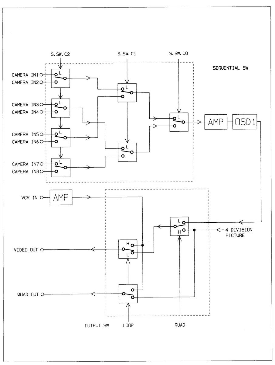
Fig. 3-7.
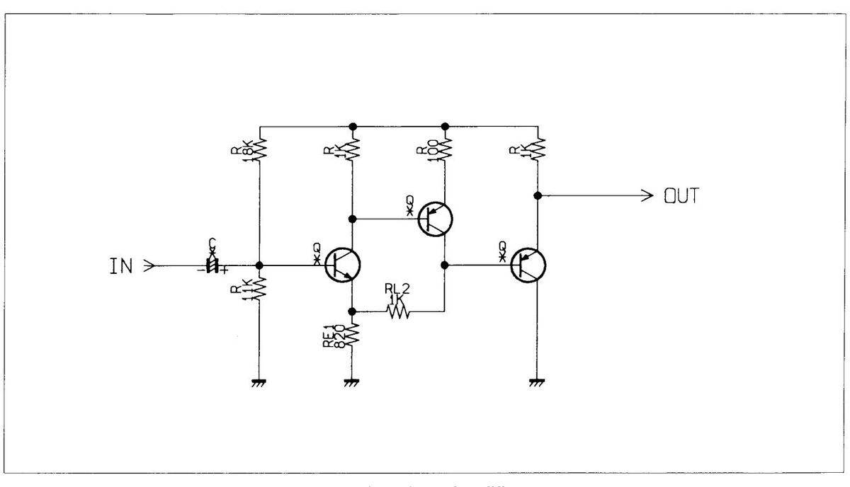
Fig. 3-8. 6 dB Amplifier
3-1-3. Decoder Circuit (VD1)
The circuit diagram, IC block diagram, terminal explanation, key signal waveforms, and filter characteristics of the decoder are shown in figures 3-9, 3-10, 3-11, 3-12, and 3-13.
«Signal Flow»
The flow of signals in the decoder are divided into the Y and C2 systems and explained below.
The picture signal, after flowing from the immediately previous switch and through the buffer, branches off in three directions.
- (1) It is amplified to 2 Vpp by the intensity system's 6 dB amplifier, the color signal is removed by the LPF, and it is passed through the buffer and output to the A D. The Y level at this point is approximately 1.3 Vpp (fig. 3-12 (b)).
- It enters pin 25 of the IC, the horizontal sync is separated, and it is output to pin 28. Based on this, the BGP is produced from pins 1 and 2. BGP width is determined by the potential at pin 2.
3 The chroma components alone are retrieved via the BGP and input into pin 6.
At that point, the burst is extracted based on the BGP, wave detection is carried out, and then amplification (ACC) is performed so that the chroma signal's level becomes constant. This ACC level is determined by the potential at pin 4. This amplified chroma signal is output from pin 3. enters pins 14 and 16. and is synchronized with the burst via VCXO. Then, based on 4Fsc from the oscillator. Fsc signals differing by 90 and 180 degrees are created, and the chroma signal is demodulated into the coloration signal. Harmonics are then removed from the separated coloring signal using the LPF, and the signal is output to the A/D via the buffer. The coloring signal level at this point is approximately 0.6-0.9 Vpp. Tint adjustment is carried out according to the potential at pin 11.
To adjust the sub-carrier, the Fsc frequency at pin 18 is regulated by turning the trimmer at pin 10.
Fig. 3-9 Decoder Circuit Diagram

Fig. 3-10. Block Diagram (M51271FP)
| Pin No. | Function |
|---|---|
| 1 | Burst gate pulse position |
| 2 | Burst gate pule width adjustment (DC) |
| 3 | Color signal output |
| 4 | ACC level adjustment (DC) |
| 5 | Color signal input |
| 6 | Input bypass capacity |
| 7 | ACC filter |
| 8 | Reference potential |
| 9 | APC filter |
| 10 | VCXO output adjustment (size) |
| 11 | Tint adjustment (DC) |
| 12 | VCXO input |
| 13 | GND |
| 14 | B-Y input (before demodulation) |
| 15 | VDD |
| 16 | R-Y input (before demodulation) |
| 17 | NTSC/PAL switch - NTSC:OPEN; PAL:GND |
| 18 | Sub-carrier output |
| 19 | B-Y output |
| 20 | R-Y output |
| 21 | Killer filter capacity |
| 22 | Killer reference filter capacity |
| 23 | BLK pulse input |
| 24 | HD pulse input |
| 25 | Sync separation video signal input |
| 26 | Sync separation feedback capacity |
| 27 | Sync separation slice level adjustment (DC) |
| 28 | Sync separation output UNUSED |
Fig. 3-11. Description of Terminals

Fig. 3-12. Component Waveforms


Fig. 3-13. (b) Effect of Decoder Y LPF
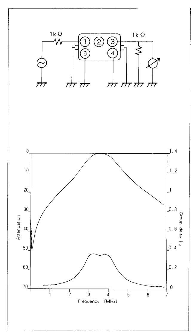
Fig. 3-13. (c) Chroma BPF 3.58 MHz ±0.5 MHz

Fig. 3-13. (d) Effect of Decoder BPF
Fig. 3-13. (e) Chroma LPF 1.3 MHz (NTSC)

Fig. 3-13. (f) Effect of Decoder C LPF
3-1-4. Encoder Circuit (VD1)
The circuit diagram, IC block diagram, terminal explanation, key signal waveforms, and filter characteristics of the encoder are shown in figures 3-14, 3-15, 3-16, 3-17, and 3-18.
«Signal Flow »
The flow of signals in the encoder are divided into the Y and C2 systems and explained below.
The paths of Y, R-Y, and B-Y, after being converted to analog signals by the immediately previous D A, are described below.
- 1 The intensity system Y signal is digitized by the equalizer and the LPF, its noise is removed, its level is adjusted using the volume, and it enters pin 36 via a coupling capacitor.
- (2) Coloration signals R-Y and B-Y are digitized by the LPF, their noise is removed, and they enter pins 29 and 31 via coupling capacitors. The signals are clamped by the pulse which regulated the horizontal sync signal input to pin 39. Fsc signals of 90 and 180 degrees are created from the free-running 4Fsc and, by AM modulating and adding these signals, an orthogonal-balance modulated chroma signal is obtained. The burst signal is then added to this, and the resulting signal is amplified, output from pin 33. It flows through the BPF, its harmonics are removed, and it is input into pin 35.
Meanwhile, the Y signal enters pin 36, its pedestal is clamped, and it is Y/C mixed. Then the C-SYNC signal which entered pin 39 is added, a center frame based on the FRAME signal from pin 40 is added, and the resulting signal is output to pin 38. From there, it passes through a buffer and is output to the OSD.
3 Meanwhile, the switcher output picture signal input into pin 2 is separated into horizontal sync and vertical sync by the sync separation circuit, and output from pin 5 and pin 8 to OSD 1.
The AFC circuit and the ACC circuit are not utilized in this configuration.
«Y-C Time Difference
Since this color quad compressor operates in component form, it requires a signal separation filter, so time reconciliation of the intensity signal and the chroma signal must be performed. Delay times are adjusted as shown below.
| Dec | oder | Digital | Enc | (Units : | |||
|---|---|---|---|---|---|---|---|
| BPF | LPF | GΑ | LPF | BPF | Total | ||
|
Chroma
signal |
350 260 | О | 260 | 350 | 1220 | ||
|
Intensity
signal |
_ | 210 | 800 | 210 | _ | 1220 | |

Fig. 3-14. Encoder Circuit Diagram
Fig. 3-15. Block Diagram
| 1 Video switch control | |||||||
| 2 Video input 1 | |||||||
| 3 Sync separation filter | |||||||
| 4 Video input 2 | Video input 2 | ||||||
| 5 Sync separation output | Sync separation output | ||||||
| 6 Timing filter | |||||||
| 7 Vertical sync separation capacitor | |||||||
| 8 Vertical sync output | |||||||
| 9 Composite sync signal output | |||||||
| 10 Horizontal sync output UNUSED | |||||||
| 11 VCO input UNUSED | |||||||
| 12 VCO output UNUSED | |||||||
| 13 AFC filter UNUSED | |||||||
| 14 NC | |||||||
| 15 Burst gate width UNUSED | |||||||
| 16 Ground 1 | |||||||
| 17 VCXO input | |||||||
| 18 Free-running control | |||||||
| 19 VCXO output | |||||||
| 20 APC filter UNUSED | |||||||
| 21 HD input NTSC PAL switch | HD input NTSC PAL switch | ||||||
| 22 ACC filter | |||||||
| 23 Main chroma input UNUSED | |||||||
| 24 Killer reference UNUSED | |||||||
| 25 Killer level UNUSED | |||||||
| 26 Killer capacitor UNUSED | |||||||
| 27 Killer output | |||||||
| 28 Power supply voltage | |||||||
| 29 R-Y input | |||||||
| 30 BFP R-Y input | |||||||
| 31 B-Y input | |||||||
| 32 BFP B-Y input | |||||||
| 33 Chroma output | |||||||
| 34 Chroma level filter | |||||||
| 35 Auxiliary chroma input | |||||||
| 36 Intensity input | |||||||
| 3/ Ground 2 | |||||||
| 38 D video output | |||||||
| 39 Composite sync signal input | |||||||
| 40 Frame insertion signal input | |||||||
| 41 Main auxiliary switch control | |||||||
| 42 Auxiliary video signal output | |||||||
Fig. 3-17. Signal Waveforms


Figure 3-18 (f) Effect of Chroma BPF
START 0. 0 MHz
Minim
₩
WHEN
SWP 30 ms
VBW 300 KH:
3-1-5 . On-screen Circuit (VD1)
As shown in diagram 3-19, this set's on-screen circuit utilizes two OSD IC M35010SP components.
OSD 1 is the component which inserts characters into digitally processed picture signals which are output from the gate array, D/A, and encoder; i.e., characters on the quad screen. The sync signals for this on-screen circuit, VD OSD and HD OSD, are created in gate array 4. In order for this HD OSD signal to compress the characters inserted on the quad screen in the vertical direction, an extra sync is inserted before the horizontal sync, as shown in figure 3-20, thus incrementing the OSDIC vertical counter and cutting the number of dots in characters in the vertical direction by half. As a result, characters with a vertical height of 16 dots are reduced to 8 dots.
OSD 2 is the component which inserts characters into full screen signals. The sync signal from the camera signal entering via the switcher is separated by the encoder's sync separation circuit, and is then used as OSD 2's external sync signal. The camera signal entering via the switcher is 1 Vpp, so it is amplified to 2 Vpp by the 6 dB amplifier, characters are inserted into it by OSD 2, and it is output.
- OSD 1 and OSD 2 functional differentiation OSD 1 … Quad screen titles and menus OSD 2 … Full screen titles and menus
- 2. Block diagram
The block diagram for the on-screen IC is shown in figure 3-21. The oscillator circuit which generates sync signals is not utilized.
The whiteness level of the insertion characters can be changed via the LECHA DC level.
HOR and VOR are negative, and AC is reset directly via the reset IC. P0 through P3 are not utilized.
The size of characters in the horizontal direction decreases when the frequency of the display's oscillator increases, and increases when this frequency decreases.
3. Microcomputer interface
This OSD IC is controlled by 8-bit serial data (CS 1, CS 2, CLK, DATA) from a microcomputer. Functional differentiation of the chip selects (CS 1 and CS 2) is as follows.
- CS 1 ... OSD 1
- CS 2 ... OSD 2
The timing of the serial data is shown in figures 3-22 and 3-23.
4. Character configuration
| Full Screen | Quad Screen | |
|---|---|---|
| Horizontal | 12 | 12 |
| Vertical | 18 | 9 (dots) |
5. Screen configuration
The screen is composed of 24 characters horizontally and 10 lines vertically, as shown in figure 3-24.
- 6. Memory configuration The configuration of the memory is as shown in figure 3-25.
- 7. Description of terminals
A description of the terminals is presented in table 3-1.
Fig. 3-19 On-Screen Circuit

Fig. 3-19. Block Diagram of Periphery of On-Screen Function

Fig. 3-20. HD Waveform for OSD IC
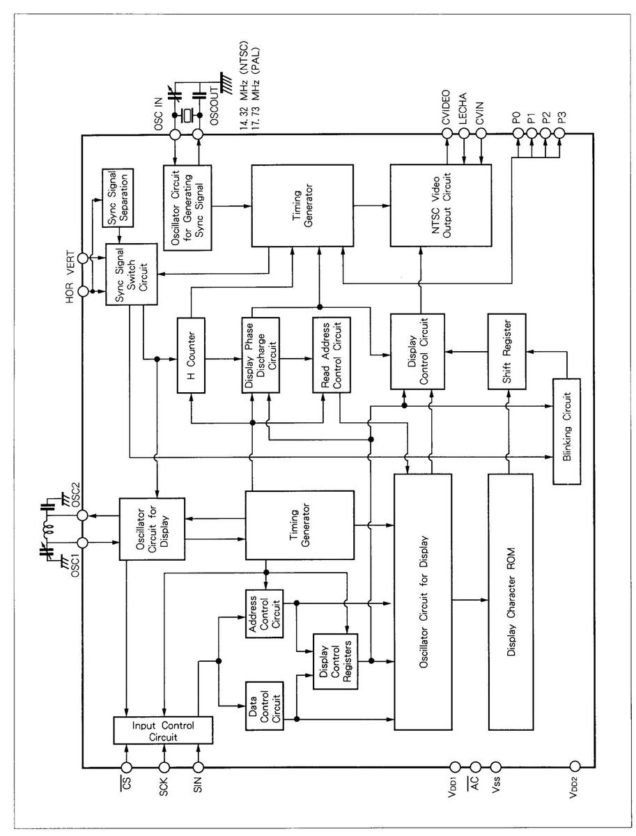
Fig. 3-21. Block Diagram (20 Pin)
Serial Data Input (Note: Timing conditions, when not specified, are Ta = -20 to + 70 °C, VDD = 5 ± 5.5 V)
| Course had a | Ratings | Linita | Natas | ||||
|---|---|---|---|---|---|---|---|
| Item | Symbols | Minimum | Standard | Maximum | Units | NOTES | |
| SCK width | t w (SCX) | 200 | _ | - | ns | ||
| CS set-up time | t su (CS) | 200 | _ | _ | ns | ||
| CS hold time | t h (CS) | 2 | - | μS | |||
| SIN set-up time | t su (SIN) | 200 | - | - | ns | ||
| SIN hold time | t n (SIN) | 200 | 200 — | ns | |||
| Single word write time | tword | 5 | - | _ | μs | ||
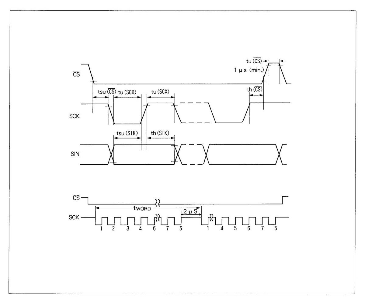
Fig. 3-22. Timing
Notes : (1) Addresses are comprised of 8 bits.
- (2) Data os cp, rosed pm 8 bits.
- (3) The 8 bits of SCK following the trailing edge of CS are taken to be the address, and this address is incremented for each 8 bits of input data thereafter.
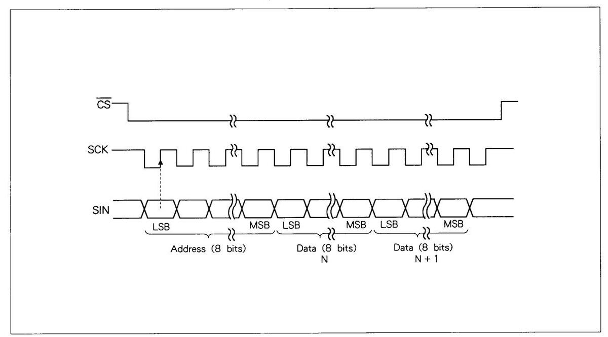
Fig. 3-23. Timing
| - Line | ə 1 | 01 | 6 JC | quen | ||||||||||||||||||||
|---|---|---|---|---|---|---|---|---|---|---|---|---|---|---|---|---|---|---|---|---|---|---|---|---|
| 1 | 0 | Т | 2 | 3 | 4 | 5 | 6 | 7 | 8 | 9 | 10 | П | 12 | 13 | 14 | 15 | 16 | 17 | 8 | | 19 | 20 | 21 | 22 | 23 |
| 24 | 25 | 26 | 27 | 28 | 29 | 30 | 31 | 32 | 33 | 34 | 35 | 36 | 37 | 38 | 39 | 40 | 41 | 42 | 43 | 44 | 45 | 46 | 47 | |
| 48 | 49 | 50 | 51 | 52 | 53 | 54 | 55 | 56 | 57 | 58 | 59 | 60 | 61 | 62 | 63 | 64 | 65 | 66 | 67 | 68 | 69 | 70 | 71 | |
| 72 | 73 | 74 | 75 | 76 | 77 | 78 | 79 | 80 | 81 | 82 | 83 | 84 | 85 | 86 | 87 | 88 | 89 | 90 | 91 | 92 | 93 | 94 | 95 | |
| 96 | 97 | 98 | 99 | 100 | 101 | 102 | 103 | 104 | 105 | 106 | |07 | 108 | 109 | 110 | ш | 112 | 113 | ||4 | 115 | 116 | 117 | 118 | 119 | |
| Lines 2 to 10 | 120 | 121 | 122 | 123 | 124 | 125 | 126 | 127 | 128 | 129 | 130 | |3| | 132 | 133 | 134 | 135 | 136 | 137 | 138 | 139 | 140 | |41 | 142 | |43 |
| 144 | 145 | |46 | |47 | 148 | 149 | 150 | 151 | 152 | 153 | 154 | 155 | |56 | 157 | 158 | 159 | 160 | 161 | 162 | 163 | 164 | 165 | 166 | 167 | |
| 168 | 169 | 170 | 171 | 172 | 173 | 174 | 175 | 176 | 177 | 178 | 179 | 180 | 181 | 182 | 183 | 184 | 185 | 186 | 187 | 188 | 189 | 190 | 191 | |
| 192 | 193 | 194 | 195 | 196 | 197 | 198 | 199 | 200 | 201 | 202 | 203 | 204 | 205 | 206 | 207 | 208 | 209 | 210 | 211 | 212 | 213 | 214 | 215 | |
| 216 | 217 | 218 | 219 | 220 | 221 | 222 | 223 | 224 | 225 | 226 | 227 | 228 | 229 | 230 | 231 | 232 | 233 | 234 | 235 | 236 | 237 | 238 | 239 |
Fig. 3-24. Screen Configuration
Description of Terminals
| Pin No. | Symbol | Terminal Name | Functional Description |
|---|---|---|---|
|
1
2 |
OSC 1
OSC 2 |
External oscillator circuit connection terminal |
External connection terminal for screen oscillator circuit.
Reference oscillator frequency is approximately 7 MHz. The horizontal display position and character width on the television screen are determined by this oscillator frequency. |
| 3 | CS | Chip select input |
Chip select terminal.
Put in 'L' state during serial data transfers. Hysteresis input. Includes pull-up resistor. |
| 4 | SCK | Serial clock input |
When the CS terminal is 'L', SIN serial data is retrieved on the leading edge of SCK.
Hysteresis input. Includes pull-up resistor. |
| 5 | SIN | Serial data input |
Display control registers, along with display data memory addresses
and data, are input serially. Hysteresis input. Includes pull-up resistor. |
| 6 | AC | Auto clear input |
In the 'L' state, resets the IC's internal circuits.
Hysteresis input. Includes pull-up resistor. |
| 7 | V DD2 | Power supply terminal | Analog-type power supply terminal. Connect to +5 V. |
| 8 | C VIDEO |
Composite video signal
output |
Terminal for output of the composite video signal.
Outputs a 2 Vpp composite video signal. When superimposing, characters are overlaid onto the composite video signal which is input from the CVIN terminal. |
| 9 | LECHA | Character level input |
Input terminal which determines the level of output characters within the composite video signal.
Character color is white. |
| 10 | CVIN | Video input |
Input terminal for external composite video signal.
When superimposing, characters are overlaid onto this external composite video signal. |
| 11 | Vss | Ground terminal | Terminal for grounding. Connect to GND. |
| 12 | PO | Port 0 output | Outputs port terminal output or character background signal (BLNK 1*). Polarity can be selected when the font ROM is specified. |
| 13 | P1 | Port 1 output |
Outputs port terminal output or character signal (CO 1*).
Polarity can be selected when the font ROM is specified. |
| 14 | P2 | Port 2 output | Outputs port terminal output or character background signal (BLNK 2*). Polarity can be selected when the font ROM is specified. |
| 15 | Р3 | Port 3 output | Outputs port terminal output or character background signal (CO 2*). Polarity can be selected when the font ROM is specified. |
|
16
17 |
OSC OUT
OSC IN |
Oscillator circuit for
sync signal |
Terminal for connection of external oscillator circuit for sync signal.
Oscillation frequency utilized is 14.32 MHz for NTSC format and 17.73 MHz for PAL format. |
| 18 | HOR* |
Horizontal sync signal
input |
Inputs the horizontal sync signal. Hysteresis input.
Polarity can be selected when the font ROM is specified. |
| 19 | VERT* | Vertical sync signal input |
Inputs the vertical sync signal. Hysteresis input.
Polarity can be selected when the font ROM is specified. |
| 20 | V DD1 | Power supply terminal | Digital-type power supply terminal. Connect to +5 V. |
Table 3-1. Description of Terminals
Memory Configuration
| DA | DA | DA | DA | DA | DA | DA | DA | Damanlar | |
|---|---|---|---|---|---|---|---|---|---|
| 7 | 6 | 5 | 4 | 3 | 2 | I | 0 | Remarks | |
| 0 | EXP | C 6 | C 5 | C4 | C 3 | C 2 | C1 | Co | |
|
Expansion
Bit |
Display RAM | ||||||||
| 239 | EXP | C 6 | C 5 | C4 | C 3 | C 2 | C1 | Co | |
| 240 | PTD | PTD | PTD | PTD | PTC | PTC | PTC | PTC | Port output |
| 3 | 2 | I | 0 | 3 | 2 | I | 0 | setting | |
| 241 | TBASE | TBASE | HP | HP | HP | HP | HP | HP | Horizontal display |
| I | 0 | 5 | 4 | 3 | 2 | I | 0 | position setting | |
| 242 | INT | SEPV | VP | VP | VP | VP | VP | VP | Vertical display |
| NON | 5 | 4 | 3 | 2 | I | 0 | position setting | ||
| 243 | VSZ | VSZ | VSZ | VSZ | HSZ | HSZ | HSZ | HSZ | Character size |
| 21 | 20 | 11 | 10 | 21 | 20 | 11 | 10 | setting | |
| 244 | DSP | DSP | DSP | DSP | DSP | DSP | DSP | DSP | Display format |
| 7 | 6 | 5 | 4 | 3 | 2 | 1 | 0 | setting | |
| 245 | N | TEST | TEST | TEST | EXP | EXP | DSP | DSP | Expansion display |
| P | 2 | Ι | 0 | 1 | 0 | 9 | 8 | setting | |
| 246 | EQP | PAL | PAL | ALL | FSC | BLINK | BLINK | BLINK | Blinking setting |
| н | 25 | 24 | 2 | I | 0 | ||||
| 247 | BLKHF | BB | BG | BR | LEVEL | PHASE | PHASE | PHASE | Raster color |
| 3 | 2 | ł | 0 | setting | |||||
| 248 | OSP | CONT | STOP | STOP | RAM | EX | BLK | BLK | Control display |
| ON | 7 F | I | IN | ERS | I | 0 |
*Upon resetting via the AC terminal, display control registers are all set to "0".
Fig. 3-25. Memory Configuration
3-2 Control Circuits
3-2-1. Buzzer Circuit (VD1)
This buzzer circuit, which utilizes as an oscillator a floating-gate-type astable multivibrator employing a CMOS NAND circuit, drives a buzzer by adding the oscillator signal to it in response to an ON signal from the microcomputer. The circuit diagram and its various waveforms are shown in figures 3-26 and 3-27. The period of the waveforms in this circuit is T = 1.38CB = 0.19 msec.
but in actuality it is approximately 0.25 msec.
When the buzzer is not being used voltage is not applied to it, and transistor 01901 is turned on (If direct voltage is continuously applied to the buzzer the possibility exists that niezoelectric elements will polarize.)
In order that the buzzer does not go on when microcomputer output is reset (when power is turned on), even if a high level is output to NAND3, this is
made a low-active output which is inverted so that the output to SW (NAND4) is high-active
As shown in the table, when IN 1 is low, the output of NAND4 is normally high and 01901 is turned on When IN 1 is low, the input to IN 2 is inverted and output. This means that 01901 is turned off and voltage is applied to the buzzer only when IN 1 and IN 2 are both high. This IN 2 input signal goes on and off every 0.125 msec. Accordingly, a frequency of approximately 4KHz is imparted on the buzzer, and the buzzer sounds
| SW ( | NAND4) | Operation |
|---|
| (NAND 3 OUT) | (OSC OUT) | OUT | BZIN |
|---|---|---|---|
| L | L | н | L |
| L | Н | Н | L |
| Н | L | Н | L |
| н | н | L | Н |
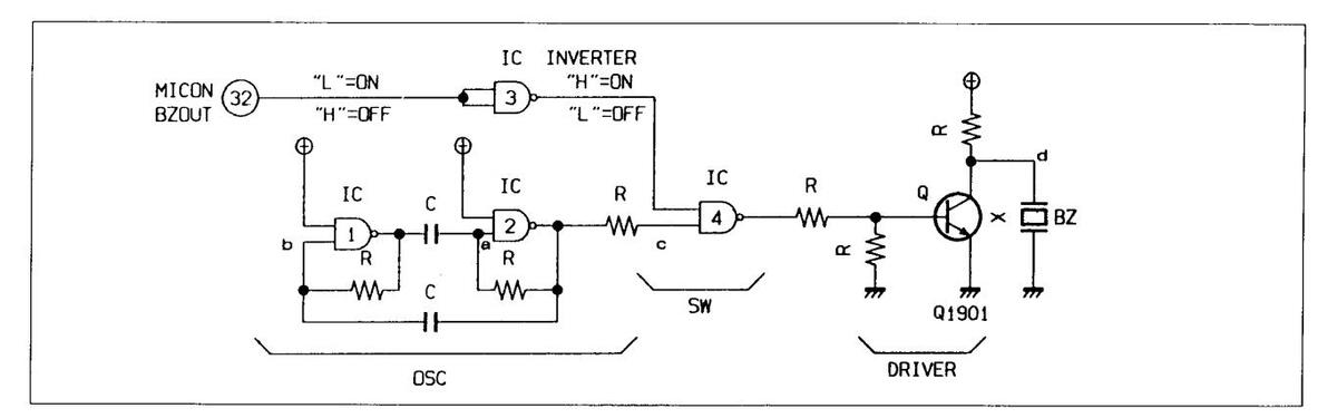
Fig. 3-26. Buzzer Circuit Diagram

Fig. 3-27. Buzzer Waveform Diagram
3-2-2. Reset Circuit (VD1)
The reset circuit for the microcomputer and the on-screen IC is implemented using an M51953A resetting IC. Its external appearance, block diagram, and operating waveform diagram are shown in figures 3-28, 3-29, and 3-30. The detection voltage for this IC is : minimum 4.05 V, standard 4.25 V, maximum 4.45 V.
《Principles of Operation》
The reference voltage (1.25 V) and the value of VDD when voltage-divided by R 1 and R 2 are compared by the hysteresis comparator and reverse-output by the output comparator. By turning off a transistor which was on, the delay capacity starts to charge to 5µA, so the voltage traces up the charging curve.
This voltage and the internal reference voltage are compared and reverse-output by the subsequent hysteresis comparator, which, by turning on the subsequent transistor, causes a low reset pulse to be output.

Fig. 3-28. External Appearance Diagram

Fig. 3-29. Block Diagram
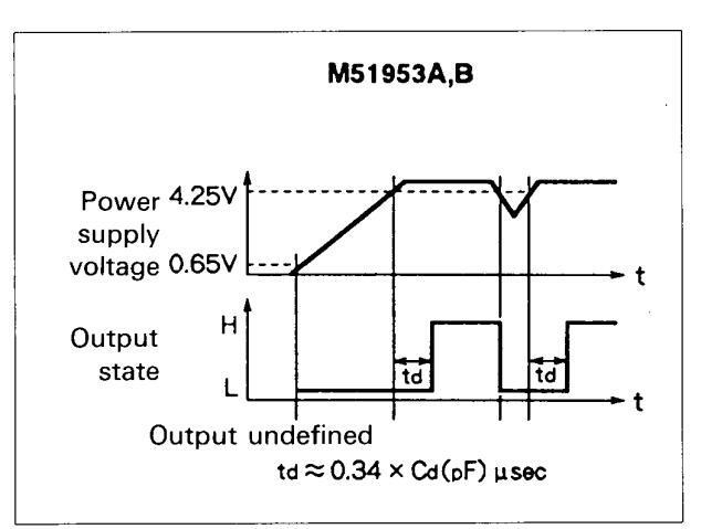
Fig. 3-30. Operating Waveform Diagram
3-2-3. EEPROM Circuit (VD1)
This memory utilizes the M6M80011AFP. The specifications for this IC are as follows. Appearance : 10-pin plastic-mold SOP IC Type : 1024-bit non-volatile memory Overwrites : 105 Data retention : 10 years A terminal description (table 3-2), block diagram (fig. 3-31.), and memory map are presented below.
(MEMORY MAP)
| 00~03 | CAMERA 1 TITLE |
|---|---|
| 04~07 | CAMERA 2 TITLE |
| 08~0B | CAMERA 3 TITLE |
| 0C~0F | CAMERA 4 TITLE |
| 10~13 | CAMERA 5 TITLE |
| 14~17 | CAMERA 6 TITLE |
| 18~1B | CAMERA 7 TITLE |
| 1C~1F | CAMERA 8 TITLE | |
|---|---|---|
| 20~21 | SEQUENTIAL SW TIME | |
| 22~23 | ZOOM POSITION | |
| 24~27 | SENSOR HORIZONTAL POSITION | |
| 28~2B | SENSOR VERTICAL POSITION | |
| 2C~2D | SENSOR LEVEL | |
| 2E | SENSOR DISPLAY BIT 4 BIT A SCREEN | |
| SENSOR DISPLAY BIT 4 BIT B SCREEN | ||
| SENSOR ON/OFF BIT 8 BIT | ||
| 2F | QUAD MODE ON A 4 BIT | |
| QUAD MODE ON B 4 BIT | ||
| ALARM MENU DATA 4 BIT | ||
| QUAD SW TIME 4 BIT | ||
| 30 | MODE 4 BIT | |
| QUAD VERTICAL POSITION | ||
| 31~3E | NO USE | |
| 3F | MEMORY OVERWRITE COMPLETION CODE | |
| ł |
Description of Terminals
| Terminal Name | Symbol | Functions |
|---|---|---|
| Chip Select Input | CS |
|
| Clock Input | SCK |
|
| Data Input | DI | • Data input is performed from this terminal. |
| Data Output | DO |
|
| Reset Input | RESET |
|
| Busy Output |
RDY/
BUSY |
|
Fig. 3-2. Description of Terminals
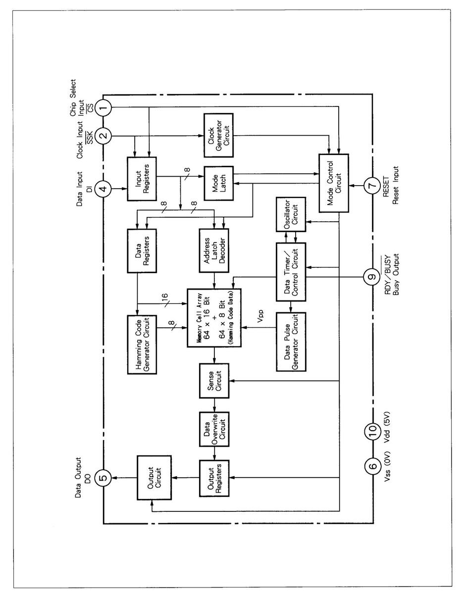
Fig. 3-31. Block Diagram
3-2-4. Remote Control Circuit (VD1)
This remote control circuit is a dual-line wired remote control of the voltage comparison variety. The circuit diagram is as shown in figure 3-33, and its various waveforms are shown in figure 3-34.
The principles of operation for this circuit are as follows. The voltage produced by the comparator is voltage-divided by the unit's resistance R0 and the external encoder resistance
The resulting voltage is compared with reference voltage Vr, which is the 4-bit up-counter output in the microcomputer after being digital/ analog-converted by an R-2R ladder network. Based on this comparison, microcomputer output bits at points of comparator output variation are determined to be encoder input, and are subsequently decoded. Normally, in this circuit, when there is no input, 4.2 V DC is output, data output from the microcomputer is periodically counted up, and input is continually compared via the comparator.
When there is a key input, the comparator produces a corresponding voltage Vin, which is compared with reference voltage Vr, and REMOTE IN goes low upon detection of the variation point. When this occurs the data is latched, and if it matches two times then it is taken to be an input.
With the remote control operation component (encoder), if the SWn key is pressed, the comparator in-phase input Vin is indicated as :
Vin = RSUM * VDD/(RSUM + R0).
When power supply voltage VDD is 5 V, this Vin's reference voltage Vr (comparator in-phase input voltage) must be made smaller than its maximum value of VDD - 1.5 V = 3.5 V. Thus, the voltage range achieved by voltage-dividing via R0 and the encoder resistance is :
0 < Vin < 3.5 V
Consequently, comparator reference voltage Vr must also be within this range.
Normally, the voltage at point R is 15 * VDD/16, and since this exceeds the above range, it must be voltage-divided by RA and RB. For RA and RB, resistors with a tolerance of 0.5 % are used. In addition, encoder resistance Ri is selected to realize a potential of between Vri and Vri + 1.
Input Voltage and Reference Voltage Vr for Keys
| KEY ON | Vin |
Reference
Voltage Vr |
D 0 | D1 | D 2 | D 3 |
|---|---|---|---|---|---|---|
| 1 | 0.124 | 0.000 | L | L | L | L |
| 2 | 0.350 | 0.232 | L | L | L | Н |
| 3 | 0.575 | 0.462 | L | L | н | L |
| 4 | 0.795 | 0.694 | L | L | н | н |
| 5 | 1.036 | 0.918 | L | Н | L | L |
| 6 | 1.280 | 1.150 | L | Н | L | Н |
| 7 | 1.493 | 1.380 | L | Н | Н | L |
| 8 | 1.719 | 1.613 | L | Н | Н | Н |
| 9 | 1.940 | 1.827 | н | L | L | L |
| 10 | 2.173 | 2.059 | н | L | L | н |
| 11 | 2.410 | 2.290 | н | L | Н | L |
| 12 | 2.622 | 2.523 | н | L | Н | н |
| 13 | 2.846 | 2.748 | н | Н | L | L |
| 14 | 3.109 | 2.981 | н | Н | L | н |
| 15 | 3.328 | 3.213 | Н | Н | Н | L |
| 3.446 | н | Н | Н | Н | ||
| OPEN | 4.12(V) | (V) |
Since resistors used for resistances R0-15 here have tolerances of ± 0.5%, a discrepancy of approximately 1% is possible for Vin and Vr above. However, since there is no area of overlap between respective Vin and Vr values, they can be adequately identified. In addition, when the remote control cable is long and its impedance is consequently high, adjust R 1 such that the combined resistance of R 1 and the circuit line is 56 Q .
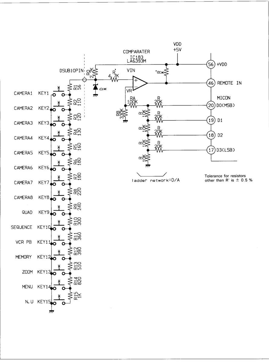
Fig. 3-33. Remote Control Circuit Diagram

Fig. 3-34. Remote Control Waveform Diagram
3-2-5. Interface Circuit (VD1)
The microcomputer interface circuit is as shown in figure 3-35.
The breakdown is :
| Alarm Input Circuit | ••• | External input : No-voltage contacts 8 |
|---|---|---|
| Internal input : Picture sensor inputs 4 | ||
| (minimum output period for | ||
| high output upon detection : 1 | ||
| field) | ||
| Switch Input Circuit | External input : No-voltage contacts 1 | |
| Alarm Output Circuit | ••• | Low output during alarms |
| Output INP 5.7 K Q (5 V) | ||
| 1.0 KΩ (0 V) |
(1) Alarm Input Circuit
For external input, a no-voltage contact is provided for each camera. When there is a low input, it is inverted to high by an inverter, passes through a diode, and enters the corresponding input port of the microcomputer. To prevent chattering on this inverted signal, a Schmidt trigger inverter is utilized. At the point of input, the two diodes are for static protection, and the capacitor is for noise cutting.
There is one internal picture sensor output for each gate array, so when using QUAD A/B mode, it is not possible to determine whether output is from cameras 1 to 4 or cameras 5 to 8. Consequently, using AND circuits, a separator divides the 4 inputs into 8 outputs. That is, using two-input one-output AND gates as shown in the truth table below, if IN 1 is high then IN 2 is output as is, and if IN 1 is low then output is low, so this effectively functions as a switch operating as an IN 1 control terminal. From a gate array, if a QUADSW input switching signal is low, cameras 1 to 4 are input, so IN 1 of AND 1 goes high, so output from AND 1 becomes active and is input to the supporting microcomputer.
| IN 1 | IN 2 | Ουτ |
|---|---|---|
| L | L | L |
| L | К | L |
| н | L | L |
| н | Н | Н |
Alarm signals from a gate array are divided from four signals to eight to realize a one-to-one correspondence with the camera signals. Subsequently, the eight internal alarm signals and the direct external alarm signals are ORed together with diodes and input to the microcomputer's respective alarm input ports. Microcomputer input is active high.
|
G.A
Output |
t |
Quad Screen
Input |
Sensor
Output |
Separator
(Microcomputer Input) |
|---|---|---|---|---|
| QUAD | L | 1 | Н | 1 |
| SW 1 | Н | 5 | 5 | |
| QUAD | L | 2 | Н | 2 |
| SW 2 | н | 6 | 6 | |
| QUAD | L | 3 | Н | 3 |
| SW 3 | н | 7 | 7 | |
| QUAD | L | 4 | Н | 4 |
| SW 4 | Н | 8 | 8 |
(2) Switching Signal Input Circuit
This switching signal circuit accepts control signals from time-lapse VTRs and the like which regulate the switch timing of sequential signals. The minimum width for switching input is one vertical interval, and switching control is performed on the falling edge of the input signal.
(3) Alarm Output Circuit
When there is an alarm input (both internal and external), during the alarm period (set by the microcomputer), an alarm out signal is output from pin 33 of the microcomputer. Microcomputer output is active low, so that alarms are not output during set start-up.
When there is a low output from the microcomputer, it is inverted to high by an inverter, and a low output is then performed by a transistor.
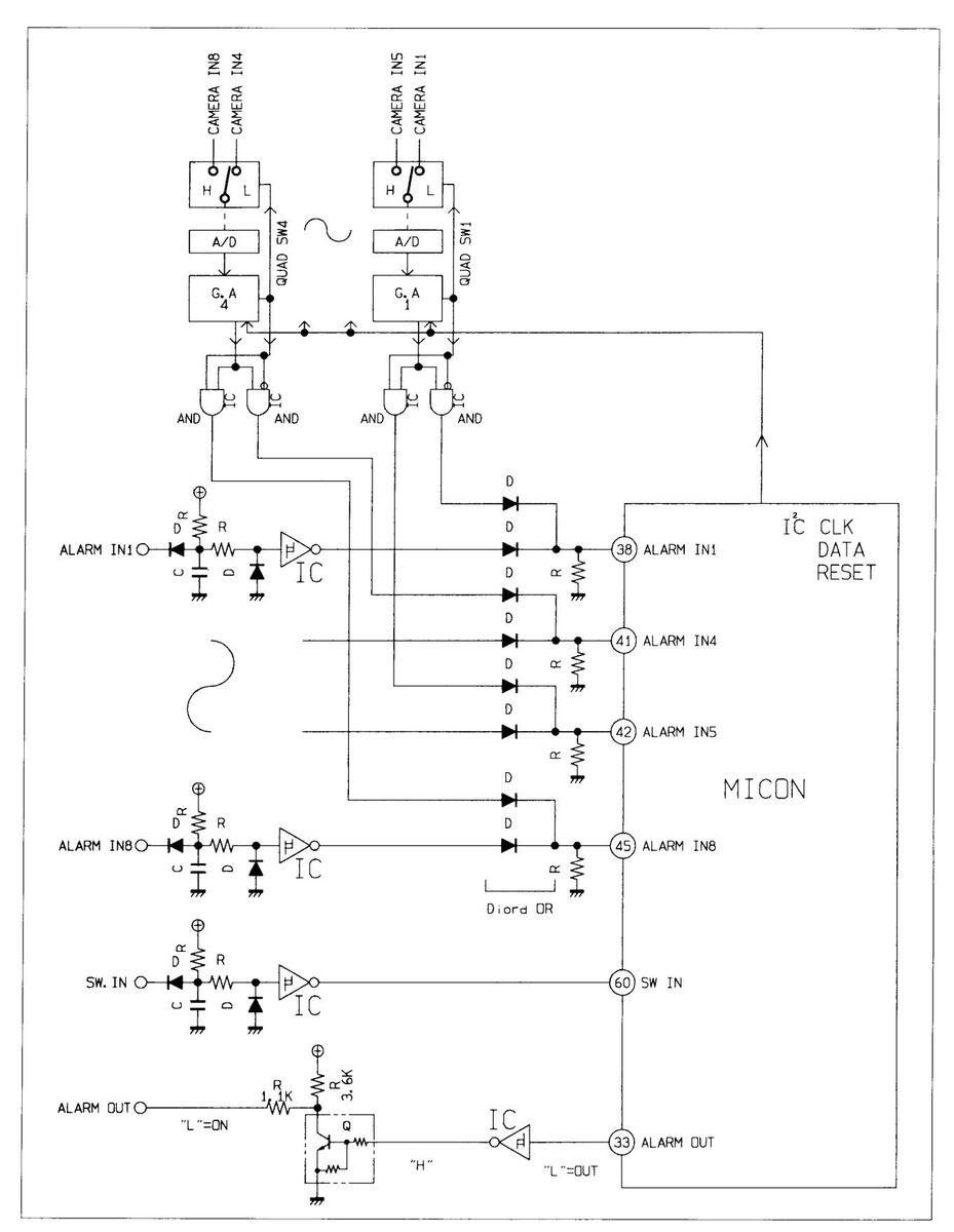
Fig. 3-35. I/O Circuit
3-2-6. System Control Circuit (VD1) «Overview»
This system controller is comprised of a single 64-pin QIP, 4-bit/chip LC66516B microcomputer with a clock frequency of 4 MHz.
Overview of Processing Functions
- Sequential switcher control
- Video output control
- Buzzer on/off control
- Remote control input decoding
- Key input control
• LED display control
- On-screen control
- EEPROM control
- Gate array control
- Switch input retrieval
- Alarm signal retrieval and output
- Signal presence/absence determination
A pin configuration diagram and a terminal description are presented in figure 3-36 and table 3-3.
《Description of Functions》
1. Sequential switcher control
This function creates and outputs a switch change-over signal which changes the input signals from among cameras 1 to 8 in accordance with the specified time and outputs them to VIDEO OUT.
Output Terminals
| Pin 21 : Seq. switch C0 (MSB) | L | L | L | L | Н | Н | Н | н | |
|---|---|---|---|---|---|---|---|---|---|
| Pin 27 : Seq. switch C1 | L | L | н | Н | L | L | Н | Н | |
| Pin 28 : Seq. switch C2 (LSB) | L | н | L | Н | L | Н | L | н | |
| Output is switched based on these 3 bits | 1 | 2 | 3 | 4 | 5 | 6 | 7 | 8 | CAMERA |
2. Video output control
This function creates and outputs a signal which controls the two outputs VIDEO OUT and QUAD ONLY OUT (see switch circuit).
Output Terminals
| VIDEO OUT | Sequential and full screen | Quad screen | VCR IN screen | VCR IN screen |
| QUAD OUT | Quad screen | Quad screen | VCR IN screen | VCR IN screen |
3. Buzzer on/off control (see buzzer circuit)
Pin 32 BZ "H" : Sound buzzer
"L" : Stop buzzer
4. Remote control input decoding
Compares the external remote control voltage with the voltage obtained by D/A conversion of count-up signals REMOTE 0-3. When the external voltage is exceeded, the REMOTE IN signal present at that time is taken as the 4-bit output to decode (see remote control circuit).
| Pin 17 REMOTE 0 (LSB) | Output |
|---|---|
| Pin 18 REMOTE 1 | Output |
| Pin 19 REMOTE 2 | Output |
| Pin 20 REMOTE 3 (MSB) | Output |
| Pin 46 REMOTE IN | Input |
5. Key input and LED display control
Mode retrieval from the front switches, and LED control. Retrieves key input status via the key matrix, and carries out dynamic pulse lighting of the LEDs via the diode matrix (see key input and LED display circuit).
- Pin 13 DIG 0 Pulse output
- Pin 14 DIG 1 Pulse output
- Pin 15 DIG 2 Pulse output
- Pin 16 DIG 3 Pulse output
- Pin 1 KEYIN 1 Key input 1
- Pin 2 KEYIN 2 Key input 2
- Pin 3 KEYIN 3 Key input 3
- Pin 4 KEYIN 4 Key input 4
- Pin 5 SEG 1 Pulse output for LED lighting
- Pin 6 SEG 2 Pulse output for LED lighting
- Pin 7 SEG 3 Pulse output for LED lighting
- Pin 8 SEG 4 Pulse output for LED lighting
6. On-screen and EEPROM control
Controls the two on-screen systems and the EEPROMs (see on-screen and EEPROM circuits).
| Pin 48 | CS 0 | Chip select for EEPROMs |
| Pin 49 | CS 1 | Chip select for on-screen ? |
| Pin 50 | CS 2 | Chip select for on-screen 2 |
| Pin 51 | CS 3 | 3 |
| Pin 9 | S. 1 | Serial input data |
| Pin 10 | S. 0 | Serial input data |
| Pin 11 | S CLK | Serial clock |
7. Gate array control and signal presence/absence determination
Carries out gate array control via l2C. A timing diagram for these signals is shown in figure 3-37, and a command list is presented in table 3-4.
Pin 57 I2C DATA IN : I2C DATA input Pin 58 I2C DATA OUT : I2C DATA output Pin 59 I2C CLK OUT : I2C clock Pin 62 I2C RESET : I2C reset Pin 53 S/N 1 : Gate array 1 signal presence/absence signal "H" : signal present Pin 53 S/N 2 : Gate array 2 signal presence/absence signal "H" : signal present Pin 54 S/N 3 : Gate array 3 signal presence/absence signal "H" : signal present Pin 55 S/N 4 : Gate array 4 signal presence/absence signal "H" : signal present
8. Switch signal and alarm signal retrieval, and alarm output
| Pin 38 | ALARM IN 1 | : Alarm signal retrieval "H" : signal present Re | cognized as camera 1 alarm |
|---|---|---|---|
| Pin 39 | ALARM IN 2 | : Alarm signal retrieval "H" : signal present Re | cognized as camera 2 alarm |
| Pin 40 | ALARM IN 3 | : Alarm signal retrieval "H" : signal present Re | cognized as camera 3 alarm |
| Pin 41 | ALARM IN 4 | : Alarm signal retrieval "H" : signal present Re | cognized as camera 4 alarm |
| Pin 42 | ALARM IN 5 | : Alarm signal retrieval "H" : signal present Re | cognized as camera 5 alarm |
| Pin 43 | ALARM IN 6 | : Alarm signal retrieval "H" : signal present Re | cognized as camera 6 alarm |
| Pin 44 | ALARM IN 7 | : Alarm signal retrieval "H" : signal present Re | cognized as camera 7 alarm |
| Pin 45 | ALARM IN 8 | : Alarm signal retrieval "H" : signal present Re | cognized as camera 8 alarm |
| Pin 33 | ALARM OUT | : Outputs "L" during alarm period | |
| Pin 60 | SW IN | : External switcher change-over signal Detects | rising and falling edges t |
determine the presence or absence of a signal.
Performs switcher change-over on either
a rising or a falling edge.
Fig. 3-36. Pin Configuration Diagram
LC665 * * Pin Configuration (1)
| Pin No. | Terminal Name | 1/0 | Output Type | Signal Name | Remarks |
| 57 | SI0/P20 | 1/0 | CMOS | I 2 C DATA | 0D |
| 58 | S00/P21 | 1/0 | CMOS | I 2 C DATA | 0D |
| 59 | SCK0/P22 | 1/0 | CMOS | I 2 C CLK | |
| 60 | INTO/P23 | I/0 | CMOS | SW IN | |
| 61 | INT1/P30 | 1/0 | CMOS | VD IN | |
| 62 | POUT0/P31 | I/0 | CMOS | I 2 C RESET | |
| 63 | POUT1/P32 | I/0 | CMOS | SET UP 1 | |
| 64 | HOLD/P33 | 1 | |||
| 1 | P40 | I/0 | MOS | KEY IN 1 | |
| 2 | P41 | I/0 | MOS | KEY IN12 | |
| 3 | P42 | 1/0 | MOS | KEY IN3 | |
| 4 | P43 | I/0 | MOS | KEY IN4 | |
| 5 | P50 | 1/0 | MOS | SEG1 | |
| 6 | P51 | 1/0 | MOS | SEG2 | |
| 7 | P52 | 1/0 | MOS | SEG3 | |
| 8 | P53 | 1/0 | MOS | SEG4 | |
| 9 | SI1/P60 | 1/0 | CMOS | S.I/0 | 0D |
| 10 | SO1/P61 | 1/0 | CMOS | S.I/0 | OD |
| 11 | SCK1/P62 | 1/0 | CMOS | S.CLK | |
| 12 | PIN1/P63 | 1/0 | CMOS | ||
| 13 | P70 | 0 | MOS | DIG 0 | |
| 14 | P71 | 0 | MOS | DIG 1 | |
| 15 | P72 | 0 | MOS | DIG 2 | |
| 16 | P73 | 0 | MOS | DIG3 | |
| 17 | P80 | 0 | CMOS | REMOTEO | |
| 18 | P81 | 0 | CMOS | REMOTE1 | |
| 19 | P82 | 0 | CMOS | REMOTE2 | |
| 20 | P83 | 0 | CMOS | REMOTE3 | |
| 21 | INT2/P90 | 1/0 | CMOS | S.SW CO | |
| 22 | TEST | 1 | |||
| 23 | VSS | I | |||
| 24 | OSC1 | Ι | |||
| 25 | OSC2 | 1 | |||
| 26 | RES | 1 | |||
| 27 | INT3/P91 | 1/0 | CMOS | S.SW C1 | |
| 28 | INT4/P92 | 1/0 | CMOS | S.SW C2 | |
| 29 | INT5/P93 | I/0 | CMOS | ZOOM | |
| 30 | PAO | 0 | MOS | OUT CONT O | (LOOP) |
| 31 | PA1 | 0 | MOS | OUT CONT 1 | (QUAD) |
| 32 | PA2 | 0 | MOS | BUZZER | |
| 33 | PA3 | 0 | MOS | ALARM OUT | |
| 34 | PBO | 0 | MOS | QUAD SW 1 | |
| 35 | PB1 | 0 | MOS | QUAD SW 2 | |
| 36 | PB2 | 0 | MOS | QUAD SW 3 | |
| 37 | PB3 | 0 | MOS | QUAD SW 4 | |
| 38 | PCO | 1/0 | CMOS | ALARM IN 1 | |
| 39 | PC1 | 1/0 | CMOS | ALARM IN 2 | |
| , |
Table. 3-3 Description of Terminals (1)
| Pin No. | Terminal Name | I/0 | Output Type | Signal Name | Remarks |
| 40 | VREF0/PC2 | I/0 | CMOS | ALARM IN 3 | |
| 41 | VREF1/PC3 | I/0 | CMOS | ALARM IN 4 | |
| 42 | CMP0/PD0 | I | ALARM IN 5 | ||
| 43 | CMP1/PD1 | l | ALARM IN 6 | ||
| 44 | CMP2/PD2 | I | ALARM IN 7 | ||
| 45 | CMP3/PD3 | I | ALARM IN 8 | ||
| 46 | TRA/PE0 | I | REMOTE IN | ||
| 47 | TRB/PE1 | Ι | SETUP 2 | ||
| 48 | POO | I/0 | MOS | CS 0 | ROM |
| 49 | PO1 | 1/0 | MOS | CS 1 | OSD 2 |
| 50 | PO2 | I/0 | MOS | CS 2 | OSD 1 |
| 51 | PO3 | I/0 | MOS | CS 3 | |
| 52 | P10 | 1/0 | MOS | S/N 1 | |
| 53 | P11 | I/0 | MOS | S/N 2 | |
| 54 | P12 | I/0 | MOS | S/N 3 | |
| 55 | P13 | I/0 | MOS | S/N 4 | |
| 56 | VDD | - |
LC665 * * Pin Configuration (2)
Table. 3-3 Description of Terminals (2)
I2C Format
The format shown in figure 3-37 is utilized for data transfers. Following the start conditions, the slave address is transmitted. This address is 7 bits long; bit 8 is the data direction bit (R/W), with 0 indicating a transfer (write) and 1 indicating a data request (read). Data transfers are always terminated via stop conditions generated by the master. If, however, the master wishes to perform further communication on the bus, it can generate start conditions and specify another slave address even if it does not first generate stop conditions. With these types of transfers, a variety of format combinations for reads and writes is possible.

Fig. 3-37. A Complete Data Transfer
QUAD I2C Definition Table
| Sub-Address | Data 8 | Data 7 | Data 6 | Data 5 | Data 4 | Data 3 | Data 2 | Data 1 | |
| PLXNT | EXXIN | FRXPL | WBGXSM | RBGXSM | FLXQD | UXD | RXL | ||
| 0 |
PAL-NTS
"H"-"L" Switch |
Read Sync
Ext/Int "H"/"L" |
Read Sync
OSC/PLL "H"/"L" |
On Writes
Enlarge/Reduce "H"/"L" |
On Reads
Enlarge/Reduce "H"/"L" |
Output Screen
Full/Quarter "H"/"L" |
Output Position
Upper/Lower "H"/"L" |
Output Position
Right/Left "H"/"L" |
|
| FILONW | PAXCH | GSON | FULLON | FILONR | WB | PH1 | PH0 | ||
| 1 |
W Vert. Filter Read Sync Mark
OFF/ON Master/Slave ON "H"/"L" "H"/"L" "H |
Marker Disp.
ON/OFF "H"/"L" |
Full Screen Out
ON/OFF "H"/"L" |
R Vert. Filter
ON/OFF "H"/"L" |
B&W/Color
"H"/"L" |
PLL Ho
Phase Ac |
rizontal
djustment |
||
| NSTILL | FSTILL | P1WR | P2WR | P3WR | P1RD | P2RD | P3RD | ||
| 2 |
Normal Still
ON/OFF "H"/"L" |
Field Still
ON/OFF "H"/"L" |
Page 1 Write
ON/OFF "H"/"L" |
Page 2 Write
ON/OFF "H"/"L" |
Page 3 Write
ON/OFF "H"/"L" |
Page 1 Read
ON/OFF "H"/"L" |
Page 2 Read
ON/OFF "H"/"L" |
Page 3 Read
ON/OFF "H"/"L" |
|
| WSTH 8 | WSTH 7 | WSTH 6 | WSTH5 | WSTH4 | WSTH3 | WSTH2 | WSTH1 | ||
| 3 | H | orizontal Writ | e Start Positio | ิวท | |||||
| WSTV8 | WSTV 7 | WSTV6 | WSTV5 | WSTV4 | WSTV3 | WSTV2 | WSTV1 | ||
| 4 | Ň | Vertical Write | Start Positior | ١ | |||||
| RSTH8 | RSTH7 | RSTH6 | RSTH5 | RSTH4 | RSTH3 | RSTH2 | |||
| 5 | 5 Horizontal Read Start Position | ||||||||
| RSTV6 | RSTV5 | RSTV4 | RSTV3 | RSTV2 | RSTV1 | ||||
| 6 | Vertical Read | Start Positior | 1 | ||||||
| GSH8 | GSH7 | GSH6 | GSH5 | GSH4 | GSH3 | GSH2 | GSH1 | ||
| 7 | Picture Sensor Horizontal Position | ||||||||
| GSV8 | GSV7 | GSV6 | GSV5 | GSV4 | GSV3 | GSV2 | GSV1 | ||
| 8 | Pi | cture Sensor | Vertical Positi | on | |||||
| CHSIG | GSF6 | GSF5 | GSF4 | GSF3 | GSF2 | GSF1 | GSF0 | ||
| 9 |
Input
Switch |
Picture Se | ensor Sensitiv | ity Setting | |||||
| CKTST | DLOFF | GSM6 | GSM5 | GSM4 | GSM3 | GSM2 | GSM1 | ||
| 10 |
Clock Test
Normal: "L" |
For B&W
Delay Off |
Picture | Sensor Mark | er Brightness | Setting | |||
| OSHD8 | OSHD7 | OSHD6 | OSHD5 | OSHD4 | OSHD3 | OSHD2 | OSHD1 | ||
| 11 | HD Phase | e Adjustment | for On-Screer | 1 Function | |||||
| PHTST | PVTST | FHTST | FVTST | FATST | MTST | PV3TST | 1W/2R | ||
| 12 |
PLL System
Horiz. Test Normal : "L" |
PLL System
Vert. Test Normal : "L" |
Read System
Horiz. Test Normal :"L" |
Read System
Vert. Test Normal : "L" |
Memory Arbiter
System Test Normal: "L" |
Memory Data
System Test Normal :"L" |
PLL System
Vert. Test 3 Normal :"L" |
Test Mode
Setting Normal :"L" |
|
Table. 3-4
3-2-7. Key Input and LED Display Circuits (SY1, 2)
This unit's key input and LED display circuits are shown in figure 3-38. These circuits are operated via microcomputer input/output carried out from the front SY1, 2 circuit board.
1. Key Input
Pulses DIG 0-3, shown in figure 3-39 (a), are output to the key matrix in figure K-1. When a key switch goes on, the corresponding output is retrieved to KEY IN 1-4. Then, based on the timing of DIG 0-3 and the signals arriving at KEY IN 1-4, the key switch that went on is identified. For example, when the MEMORY switch is pressed, a DIG 3 pulse passes through a diode and through the MEMORY switch, and goes into KEY IN 1. If two DIG 3 pulses in a row go in, the MEMORY switch is identified as the key that was pressed.
Figure 3-39 (b) shows the identification of the key at the point when these pulses arrive at KEY IN
1-4. In addition, only immediately after the microcomputer is reset, the SETUP pulse at pin 63 is output and read-in of the initial settings is performed.
2. LED Driver Circuit
LEDs are driven using dynamic pulse lighting, and light up when both SEG 1-4 and DIG 0-3 are high.
If the positions representing SEG 1 and DIG 3 go on, for example, a pulse passes through a buffer and heads for four locations : CAMERA 1, CAMERA 5, QUAD, and MEMORY. Among transistors Q0-3, however, the only one which is on is Q3, so current flows to the MEMORY LED and this LED lights up. Figure 3-39 (c) shows the LED which lights up when the lighting pulse is output to SEG 1-4. When lighting is to be continuous, repeated output of these DIG and SEG pulses is performed periodically.
Fig. 3-38. Key Input and LED Display Circuit Diagram


Fig. 3-39. (b) KEY IN Input Waveforms and Read-In
Fig. 3-39. (c) SEG Output Waveforms and Lit LED
3-3. Digital Circuits
3-3-1. A/D Converter Circuit (IC211, IC221, IC231, IC231, IC241) (VD1)
The intensity signal and coloration signals (R-Y, B-Y) from the decoder are A/D-converted by a 6-bit A/D converter (µPC 661 parallel-comparison A/D converter) which includes an internal analog multiplexer with clamping capability on each of its four inputs. A block diagram of this IC is presented in figure 3-40.
The intensity signal and coloration signals (R-Y, B-Y), which are respectively input to pins 16, 17, and 18, are first clamped by the clamp circuit.
Multiplexing is then performed by the internal multiplexer in "Y, R-Y, Y, B-Y, Y,..." format. The timing chart for this is shown in figure 3-2.
The multiplexed signal is converted into digital data by the 6-bit A/D converter and output from pins 2 (LSB) to 7 (MSB).
Control of this multiplexer is carried out via pin 11 (MPX B), pin 12 (MPX R), and pin 13 (MPX Y).
Auxiliary clamping operations are also performed.
Firstly, for the intensity signal, while the clamp pulse at pin 9 is high, the signal voltage which has been input to pin 16 is clamped to make it equal to VRT (the reference top voltage) at pin 20. This is illustrated in figure 3-42. Next, similarly for the coloration signals as well, while the clamp pulse is high, the signals which have been input to pins 17 and 18 are clamped to make them equal to VRM (the reference midpoint voltage) at pin 20.
The A/D clock frequency in every mode is 20 MHz. For reduction, however, since the gate array data is thinned out, the effective frequency is as shown in table 3-5.
| Y Clock | R-Y Clock | B-Y Clock | |
|---|---|---|---|
| Reduction | 5MHz | 2.5MHz | 2.5MHz |
| 1:1 | 10MHz | 5MHz | 5MHz |
| ZOOM | 10MHz | 5MHz | 5MHz |
Table. 3-5
Fig. 3-40. A/D Converter Circuit

Fig. 3-41. A/D Converter Timing Chart
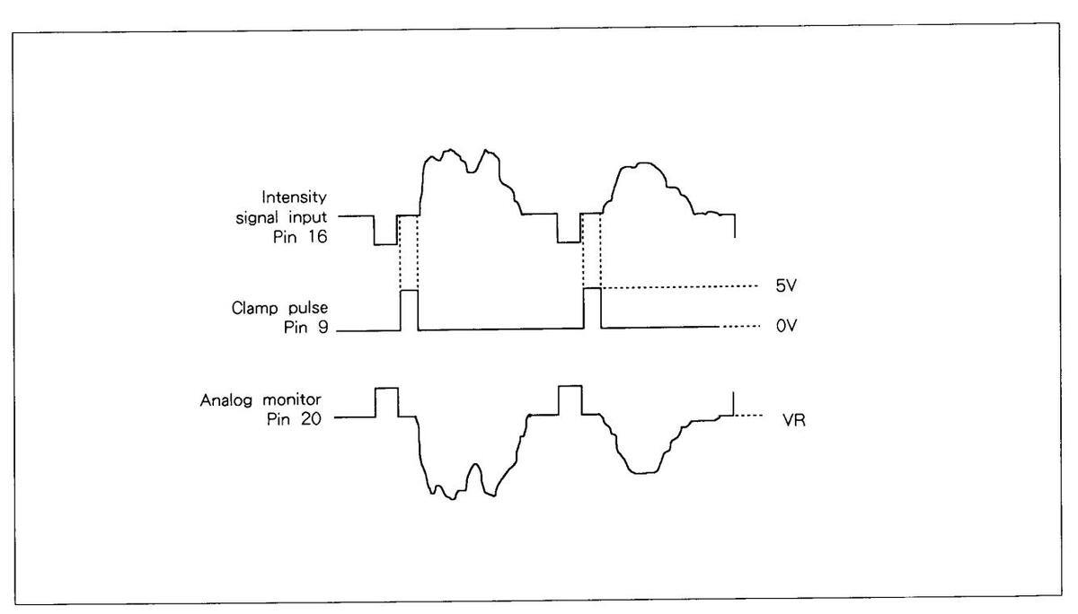
Fig. 3-42. Clamping at the Pedestal Level: Timing and Voltage Levels
3-3-2 D/A Converter Circuit (IC251) (VD1)
The 6-bit digital data from each of four respective gate arrays is sent on the same line utilizing time-division multiplexing. Synchronization thereof is performed based on the CLK, HD, and VD signals which are output from gate array IC243.
The 6-bit digital data sent in this fashion is D/ A-converted by a D/A converter unit (M52682FP, current-adding method) which contains three 6-bit high-speed D/A converters. A block diagram for this IC is shown in figure 3-43. The 6-bit digital data is input to pins 3 (LSB) to 8 (MSB).
Since there is a single common input for all three D/A converters, the multiplexed intensity signal and coloration signals (B-Y, R-Y) are separated by shifting the phase of the clock signals which are input to pin 10 (B-Y clock), pin 11 (R-Y clock), and pin 12 (intensity signal clock). Once converted to analog form, the respective signals are then output to pin 17 (intensity signal), pin 19 (B-Y), and pin 21 (R-Y).
The clock signals for pins 10 to 12 are output from IC243, while the blanking pulse for pin 15 is output
from IC233. The function of the blanking signal is to make the DC levels of Y, R-Y, and B-Y uniform by clamping them via the encoder. The various waveforms are illustrated in figure 3-44.
Figure 3-45 presents a timing chart of the conversion of the component signals. As shown in this figure, for the intensity signal and the coloration signals, the rising edge of the signals which are input to each of the respective clock input terminals is utilized to latch the digital data and convert it to analog data.
The D/A clock frequency in every mode is 20 MHz. For zooming, however, since the same data is output twice, the effective frequency is as shown in table 3-6.
| Y Clock | R-Y Clock | B-Y Clock | |
|---|---|---|---|
| Reduction | 10MHz | 5MHz | 5MHz |
| 1:1 | 10MHz | 5MHz | 5MHz |
| ZOOM | 5MHz | 2.5MHz | 2.5MHz |
Table. 3-6

Fig. 3-43. IC252 D/A Converter

Fig. 3-44. D/A Output
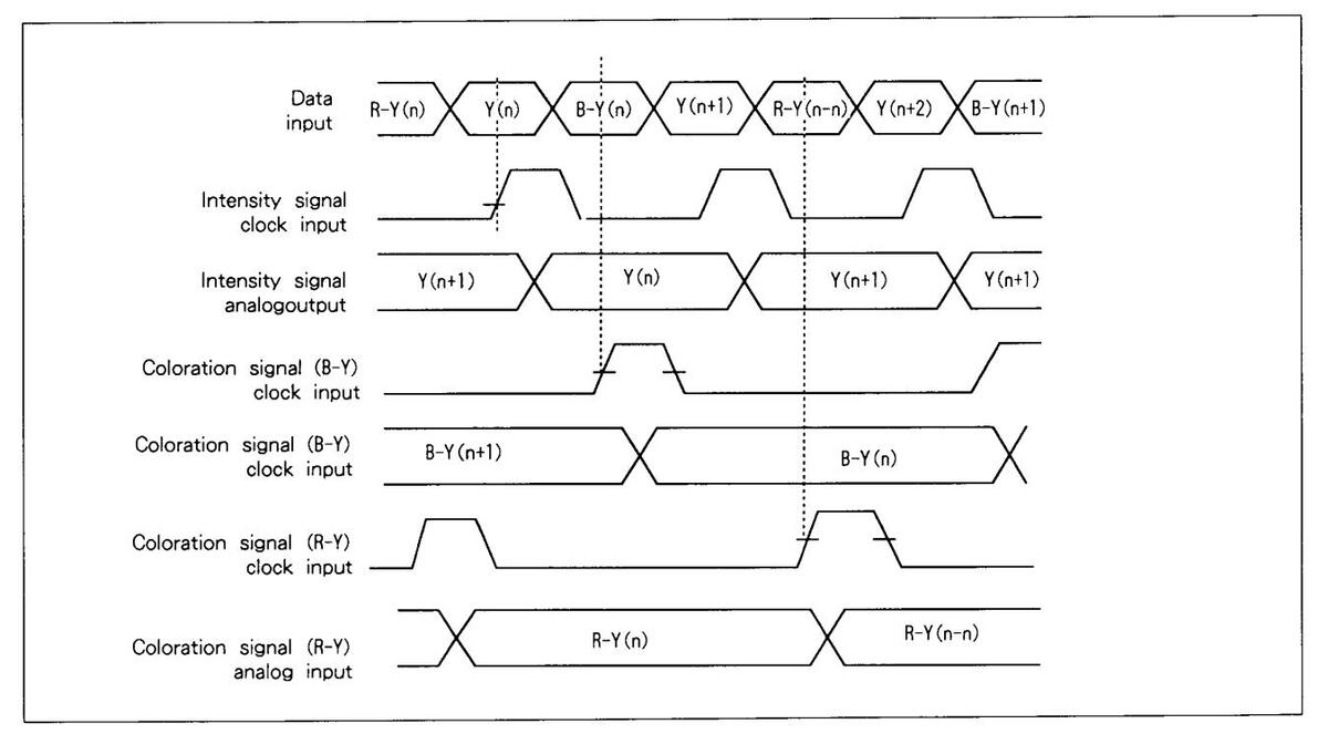
Fig. 3-45. D/A Converter Timing Chart
3-3-3. Gate Array Circuit (VD1)
1. Basic Features
Structure : 120-pin QFP, 7000 gates Process : 1.2 µm CMOS
Utilizes Seiko Epson gate array SLA860S
Supports PAL and NTSC
Digital control via I2C bus
Sync separation, built-in horizontal PLL and VCO System clock frequency : 1270 fH (approx. 20 MHz)
| Sampling Frequency | Samp | lina | Frequency |
|---|
| Normal | Enlarged | |
|---|---|---|
| Intensity signal | 5.0 MHz | 10.0 MHz |
| Coloration signal | 2.5 MHz | 5.0 MHz |
When supporting NTSC : 3-field recording method When supporting PAL : 2-field recording method Memory used : Mitsubishi M5M4C500AL (256 columns * 320 rows)
Recording Range :
| NTSC | PAL | |
|---|---|---|
| Horiz. direction | 256 dots | 256 dots |
| Vert. direction | 106 dots | 140 dots |
Contrast : 6 bits
Single-channel decoder output signals for both A/D (MPC661G) and D/A (M52682) :
HD pulse, clamp pulse
Encoder output signals :
HD pulse, composite sync signal, vertical sync signal, burst gate pulse, border pulse, blank pulse
Vertical LPF for line memory
Built-in phase reconciliation circuit for decoder and encoder intensity and coloration signals
Other features :
- (1) Enlargement during memory writes and memory reads
- (2) Horizontal write start position, vertical write start position, horizontal read start position and vertical read start position are all variable
- (3) Frame still and field still are possible Frame still ---- high resolution Field still --> page-by-page read and write are possible (3 pages for NTSC, 2 pages for PAL)
(4) Picture sensor utilizing frame correlation
(Signal Flow)
In the A/D converter, the picture signal, which was digitized via the clock and locked onto the horizontal sync signal, is temporarily taken into the gate array. It is then written to memory after write vertical LPF. picture sensor, and other processing is performed. The picture signal written to the memory in this fashion is then retrieved in sync with the crystal oscillator used for data read-out, and input to the gate array. Within the gate array, the read vertical LPF phase reconciliation, multiplexing, and other processing is performed, and the signal is input to the D/A converter.
During exchanges of data between the various devices, the transfer rate differs according to the mode. The multiplexing method, however, is always the same, and is presented below.
● A/D → Gate Array
| Y R-Y Y B-Y Y R-Y | Υ | R-Y | Υ | B-Y | Y | R-Y |
|---|
● Gate Arrav → Memory
Y memory and C memory share a common data line, and write operations are divided using the clock
| Υ | R-Y | / Y B-Y | Y | R-Y | |
|---|---|---|---|---|---|
|
↑
Y memory write clock |
↑
G memory write |
↑
Y memory write |
↑
G memory write |
↑
Y memory write |
↑
G memory write |
● Memory --> Gate Array
| Y memory output | Υ | Υ | Υ | Υ | Υ |
|---|---|---|---|---|---|
| C memory output | R-Y | B-Y | R-Y | B-Y | R-Y |
• Gate Array D/A
The D/A has three channels sharing the same data line, with data separation performed via the clock signal.
This data line is also connected to four gate arrays, with tri-state control utilized to avoid data collisions
| Υ | R-Y | Υ | B-Y | Υ | R-Y |
|---|---|---|---|---|---|
| ↑ | ↑ | ↑ | ↑ | ↑ | ↑ |
| Y data | R-Y data | Y data | B-Y memory | Y data | R-Y data |
| clock | clock | clock | clock | clock | clock |

Fig. 3-46. Block Diagram of Digital Components
2. Pin Configuration Table
| Pin No. | Pin Name | PAD | I/0 | CELL | Remarks |
|---|---|---|---|---|---|
| 1 | HD | 1 | В | BC1 | Read horizontal sync input/output |
| 2 | VSS | 2 | GND | ||
| 3 | CLKOUT | 3 | 0 | TB2 | Read clock output |
| 4 | CLKIN | 4 | I | IBC | Read clock input |
| 5 | AD1 | 5 | |||
| S | S | S | IBT | A/D data input AD1 → MSB | |
| 10 | AD6 | 10 | |||
| 11 | MPXB | 11 | 0 | OB2 | A/D multiplexer B-Y select |
| 12 | MPXY | 12 | 0 | OB2 | A/D multiplexer Y select |
| 13 | MPXR | 13 | 0 | OB2 | A/D multiplexer R-Y select |
| 14 | CLMP | 14 | 0 | OB2 | Clamp output for A/D |
| 15 | ADCLK | 15 | 0 | OB2 | A/D clock output |
| 16 | HASY | 17 | 0 | TB2 | PLL phase comparison output |
| 17 | STSY | 18 | 0 | TB2 | PLL phase comparison output |
| 18 | VDD | 19 | POWER | ||
| 19 | PDO | 20 | 0 | INI. A | PLL integrator output |
| 20 | PDI | 21 | 1 | INI. XA | PLL integrator input |
| 21 | CMTEST | 22 | Ι | IBC | Comparator test (normal : "L") |
| 22 | HSEP 2 | 23 | 0 | SAN1.ZX | Horizontal sync separation recharge current output terminal |
| 23 | VIDI | 24 | 1 | SAN1.A | Horizontal sync separation input terminal |
| 24 | HSEP 1 | 25 | 0 | SAN1.XA | Horizontal sync separation LPF inverter amp output |
| 25 | SLO | 26 | 0 | IN1.XA | Slice level setting interter output |
| 26 | SLI | 27 | Ι | IN1.A | Slice level setting interter input |
| 27 | VSEP | 28 | 0 | SAN2.XA | Vertical sync separation LPF inverter amp output |
| 28 | VSYI1 | 29 | Ι | SAN2.A | Vertical sync separation input terminal |
| 29 | VSS | 30 | GND | ||
| 30 | KILJD | 31 | Ι | INI.A | Synchronous/asynchronous discrimination input |
| 31 | VDD | 33 | POWER | ||
| 32 | VSS | 34 | GND | ||
| 33 | VC00 | 35 | 0 | IN2.XA | Inverter amp output terminal for VCO |
| 34 | VCOI | 36 | I | IN2.A | Inverter amp input terminal for VCO |
| 35 | VSS | 37 | GND | ||
| 36 | VDD | 38 | POWER | ||
| 37 | HYS | 39 | 0 | TB2 | Output terminal for synchronous/asynchronous discrimination circuit |
| 38 | HILOF | 40 | 0 | TB2 | Output terminal for synchronous/asynchronous discrimination circuit |
| 39 | KILON | 41 | 0 | TB2 | Output terminal for synchronous/asynchronous discrimination circuit |
| 40 | CSY01 | 42 | 0 | OB2 | Horizontal sync signal output |
| 41 | HDDEC | 43 | 0 | OB2 | HD pulse output for decoder |
| 42 | CLKBY | 44 | 0 | TB2 | B-Y clock for D/A |
| 43 | CLKRY | 45 | 0 | TB2 | R-Y clock for D/A |
| 44 | CLKY | 46 | 0 | TB2 | Y clock for D/A |
| 45 | BLKXVD | 47 | 0 | OB2 | Main address 3 → read VD2 → read blank pulse |
| 46 | CSYXBG | 48 | 0 | OB2 | Main address 3 → read burst gate 2 → read CSYNC |
Fig. 3-7. Pin Configuration Table (1)
| Pin No. | Pin Name | PAD | 1/0 | CELL | Remarks |
|---|---|---|---|---|---|
| 47 | WKXOS | 49 | В | BC1 | Main address 3 → read clock input → read border |
| 48 | HENXHD | 50 | 0 | OB2 | Main address 3 → read on-screen HD2 → encoder HD |
| 49 | SDA | 51 | В | BC2 | I 2 C bus data line |
| 50 | VSS | 52 | GND | ||
| 51 | DA6 | 53 | |||
| S | S | S | 0 | TB2 | D/A input data DA6 → LSB |
| 53 | DA4 | 55 | |||
| 54 | VSS | 56 | GND | ||
| 55 | DA3 | 57 | |||
| 5 | Ś | S | 0 | TB2 | D/A input data DA1 → A MSB |
| 57 | DA1 | 59 | |||
| 58 | SOCC | 60 | 0 | OB2 | Memory output clock for coloration |
| 59 | VSS | 61 | GND | ||
| 60 | VDD | 62 | POWER | ||
| 61 | SCL | 64 | I | IBS | I 2 C bus clock line |
| 62 | RSTCK | 65 | 1 | IBC | Clock system reset input "H" to reset |
| 63 | RESET | 66 | I | IBS | Gate array reset "L" to reset |
| 64 | ADR2 | 67 | 1 2 C bug main address setting | ||
| S | S | S | IBC | ||
| 65 | ADR1 | 68 | |||
| 66 | SIDC1 | 69 | Coloration memory output data | ||
| 5 | IBC | SIDC 1 → MSB | |||
| SIDCO | 74 | ||||
| 12 | LDIT | /5 | Line memory output data | ||
| 75 |
)
78 |
вс | LDI 1 → MSB | ||
| 76 | 80 | ||||
| 1 | IBC | Line memory output data | |||
| 77 | LDI6 | 81 | LDI 6 → LSB | ||
| 78 | SIGNA | 82 | О | OB2 |
Input presence/absence determination output "L" → absent "H"
→ present |
| 79 | SENSO | 83 | 0 | OB2 | Picture sensor output "L" → not operating "H" → operating |
| 80 | SICC | 84 | 0 | OB2 | Coloration memory input clock |
| 81 | RAS | 85 | 0 | OB2 | Memory control output (common Y/C) |
| 82 | IRS | 86 | 0 | OB2 | Memory control output (common Y/C) |
| 83 | VSS | 87 | GND | ||
| 84 | LDO1 | 88 | |||
| S | S | S | 0 | OB2 | |
| 88 | LDO5 | 92 | |||
| 89 | VDD | 93 | POWER | ||
| 90 | LDO6 | 94 | 0 | OB2 | Line memory input data LSB |
| 91 | VSS | 96 | GND | ||
| 92 | VDD | 97 | POWER | ||
| 93 | IR7XA7 | 98 | |||
| S | S | S | 0 | OB2 | Memory control output (common Y/C) |
| 99 | IR1XA1 | 104 | |||
| 100 | A8XAOS | 105 | 0 | OB2 | Memory control output (common Y/C) |
| 101 | VDD | 106 | POWER |
Fig. 3-7. Pin Configuration Table (2)
| Pin No. | Pin Name | PAD | I/0 | CELL | Remarks | |
|---|---|---|---|---|---|---|
| 102 | LCK | 107 | 0 | OB2 | Clock for line memory | |
| 103 | LRST | 108 | 0 | OB2 | Line memory reset | |
| 104 | SICY | 109 | 0 | OB2 | Intensity memory input clock | |
| 105 | SOCY | 110 | 0 | OB2 | Intensity memory output clock | |
| 106 | SOD1 | 111 | Memory input data (common Y/C) | |||
| S | S | S | 0 | OB2 | SOD 1 → MSB | |
| 111 | SOD6 | 116 | ||||
| 112 | SIDY6 | 117 | Intensity memory output data | |||
| S | S | S | I | IBC | ||
| 117 | SIDY1 | 122 | ||||
| 118 | VD | 123 | В | BC1 | Read vertical sync input/output | |
| 119 | VDD | 124 | POWER | |||
| 120 | CHGO | 125 | 0 | Signal switch output | ||
Fig. 3-7. Pin Configuration Table (3)
Notes : Input/output cell functional description
©Bidirectional terminals
BC1 : CMOS level input/output cell
BC2 : CMOS level input/output cell (for l22C' SDA)
◎Input terminals
IBC : CMOS level input cell
IBT : TTL level input cell
IBS : Schmidt trigger input cell (for l22C' SCL)
Output terminals
OB2 : Output cell
TB2 : Tri-state output cell
QUAD I22C Definition Table
| Sub-Address | Data 8 | Data 7 | Data 6 | Data 5 | Data 4 | Data 3 | Data 2 | Data 1 | |
| PLXNT | EXXIN | FRXPL | WBGXSM | RBGXSM | FLXQD | UXD | RXL | ||
| 0 |
PAL-NTS
″H″-″L″ Switch |
Read Sync
Ext/Int "H"/"L" |
Read Sync
OSC/PLL "H"/"L" |
On Writes
Enlarge/Reduce "H"/"L" |
On Reads
Enlarge/Reduce "H"/"L" |
Output Screen
Full/Quarter "H"/"L" |
Output Position
Upper/Lower "H"/"L" |
Output Position
Right/Left "H"/"L" |
|
| FILONW | PAXCH | GSON | FULLON | FILONR | WB | PH1 | РНО | ||
| 1 |
W Vert. Filter
OFF/ON "H"/"L" |
Read Sync
Master/Slave "H"/"L" |
Marker Disp.
ON/OFF "H"/"L" |
Full Screen Out
ON/OFF "H"/"L" |
R Vert. Filter
ON/OFF "H"/"L" |
B & W/Color
"H"/"L" |
PLL Horizo
Position A |
ontal
djustment |
|
| NSTILL | FSTILL | P1WR | P2WR | P3WR | P1RD | P2RD | P3RD | ||
| 2 |
Normal Still
ON/OFF "H"/"L" |
Full Still
ON/OFF "H"/"L" |
Page 1 Write
ON/OFF "H"/"L" |
Page 2 Write
ON/OFF "H"/"L" |
Page 3 Write
ON/OFF "H"/"L" |
Page 1 Read
ON/OFF "H"/"L" |
Page 2 Read
ON/OFF "H"/"L" |
Page 3 Read
ON/OFF "H"/"L" |
|
| WSTH 8 | WSTH 7 | WSTH 6 | WSTH 5 | WSTH 4 | WSTH 3 | WSTH 2 | WSTH 1 | ||
| 3 | Horizontal Wri | te Start Positio | n | ||||||
| WSTV 8 | WSTV 7 | WSTV 6 | WSTV 5 | WSTV 4 | WSTV 3 | WSTV 2 | WSTV 1 | ||
| 4 | Vertical Write | Start Position | |||||||
| RSTH 8 | RSTH 7 | RSTH 6 | RSTH 5 | RSTH 4 | RSTH 3 | RSTH 2 | |||
| 5 | Horizor | ntal Read Start | Position | ||||||
| RSTV 6 | RSTV 5 | RSTV 4 | RSTV 3 | RSTV 2 | RSTV 1 | ||||
| 6 | Vertical Read Start Position | ||||||||
| GSH 8 | GSH 7 | GSH 6 | GSH 5 | GSH 4 | GSH 3 | GSH 2 | GSH 1 | ||
| 7 | Pi | cture Sensor H | orizontal Positi | on | J | ||||
| GSV 8 | GSV 7 | GSV 6 | GSV 5 | GSV 4 | GSV 3 | GSV 2 | GSV 1 | ||
| 8 | Picture Sensor Vertical Position | ||||||||
| CHSIG | GSF 6 | GSF 5 | GSF 4 | GSF 3 | GSF 2 | GSF 1 | GSF 0 | ||
| 9 | Input Switch | Picture S | ensor Sensitivi | ty Setting | J | ||||
| CKTST | DLOFF | GSM 6 | GSM 5 | GSM 4 | GSM 3 | GSM 2 | GSM 1 | ||
| 10 | Clock Test | For B & W | • | ······ | |||||
| Normal : "L" | Delay Off | Pictur | e Sensor Mark | er Brightness S | etting | ||||
| OSHD 8 | OSHD 7 | OSHD 6 | OSHD 5 | OSHD 4 | OSHD 3 | OSHD 2 | OSHD 1 | ||
| 11 | HD Phase Adjustment for On-Screen Function | ||||||||
| PHTST | PVTST | FHTST | FVTST | FATST | MTST | PV3TST | 1W/2R | ||
| 12 |
PLL System
Horiz. Test Normal : "L" |
PLL System
Vert. Test Normal : "L" |
Read System
Horiz . Test Normal : "L" |
Read System
Vert. Test Normal : "L" |
Memory Arbiter
System Test Normal : "L" |
Memory Data
System Test Normal : "L" |
PLL System
Vert. Test 3 Normal : "L" |
Test Mode
Setting Normal : "L" |
|
Table. 3-8. QUAD I2C Definition Table
3 Eunctional Description of I2C Bus
PLXNT ; Switches between PAL mode and NTSC mode
"H" for PAL mode
"L" for NTSC mode
EXXIN : Switch for read sync mode. The gate array for which this goes high outputs the clock, HD, and VD signals which are used by the other gate arrays as the reference for memory reads. Accordingly, EXXIN can only go high for one gate array. FXXIN = "H" → Output the clock, HD, and VD signals from the CLKOUT, HD, and VD
terminals FXXIN = "I" → Receive the HD and VD signals from the HD and VD terminals. The CLKOUT terminal is "Hi-Z" In either case, the CLKIN terminal is the
read clock input terminal
- FRXPL ; Specifies whether to take the clock. which is output by the gate array for which EXXIN has gone high, from the external oscillator or from the PLL FRXPL = "H" → External oscillator. FRXPL = "L" → PLL.
-
WBGXSM ; Write enlargement setting. WBGXSM = "H" -> Write one-quarter of the full screen input picture signal to memory (see figure 1). Intensity signal sampling frequency :
- 10 0 MHz Coloration signal sampling frequency :
- 5 0 MHz WBGXSM = "L" -> Store the entire input
-
picture signal to memory (see figure 2).
- Intensity signal sampling frequency : 50 MHz
- Coloration signal sampling frequency : 2.5 MHz
RBGXSM; Read enlargement setting.
- RBGXSM = "H" → For guad output, output one-quarter of the data stored in memory to one-quarter of the output screen ; for full screen output, output all of the data stored in memory to the entire output screen (see fig. 3)
-
BBGXSM = "I" → Only valid for quad output : output the data stored in memory to one-quarter of the output screen (see fig. 4).
- For full screen output, RBGXSM must be high for the gate array which outputs the picture signal.
FLXOD : Switch which selects full screen output or quad output. FLXQD = "H" → Full screen output mode. FLXQD = "L" → Quad screen output mode.
FLXOD must be the same for all gate arravs
: For guad screen output, specifies whether UXD to output to the upper or lower portion of the screen.
UXD = "H" Output to upper portion of screen
UXD = "L" → Output to lower portion of screen
BXI · For guad screen output specifies whether to output to the right or left side of the screen UXD = "H" → Output to right side of
screen
UXD = "L" → Output to left side of screen.
- FILLONW : On/off state of vertical filter during writes. FILLONW = "H" → Write vertical filter off. FILLONW = "L" → Write vertical filter on.
- PAXCH : Selects whether to enable or disable terminals DA 1-6 during the "border interval" and "blanking interval." The gate array for which PAXCH = "H" outputs data to the D/A during the "border interval" and "blanking interval." Accordingly, PAXCH can only go high for one gate array.
- GSON : On/off state of marker for picture sensor. When GSON = "H" the marker is displayed. Even when the marker is not displayed, the picture sensor is operating.
- FULLON : For full screen display, the gate array for which FULLON = "H" outputs the picture signal.
- FILLONR : When WBGXSM = "H", specifies the on/ off state of the vertical LPF during memory reads FILLONR = "H" represents the on state
- ; Specifies the polarity of CSYNC output. WB WB = "H" represents positive, while WB = "L" represents negative. ; PLL phase adjustment.
PH1,
- РНО
- NSTILL ; On/off state of stills using two fields' worth of memory. NSTILL = "H" represents the on state.
- FSTILL : On/off state of stills using one field's worth of memory. TSTILL = "H" represents the on state
- P1WR : When FSTILL = "H", specifies the page to write. For page 1, for example, the instantaneous field is written to memory
- P3WR when P1WR rises from "L" to "H".
- ; When FSTILL = "H", specifies the page to read. For example, if P1RD = "H" then חסנס page 1 is read
- WSTH : Specifies, in the horizontal direction, the 8~1 dot from which to start writing the input
- picture signal to memory. WSTH 1 → LSB : WSTH 8 → MSB. WSTH 1 represents 2/1270 H. (H is the length of the horizontal interval.)
- WSTV ; Specifies, in the vertical direction, the line 8~1 from which to start writing the input
- picture signal to memory. WSTV 1 -> ISB · WSTH 8 -> MSB WSTV 1 represents 1/525 V (for NTSC) or 1/625 (for PAL) (V is the length of the vertical interval.)
- RSTH ; Specifies, in the horizontal direction, the
- 8~1 dot from which to start reading the input picture signal from memory. RSTH 2 → LSB ; RSTH 8 → MSB. RSTH 2 represents 4/1270 H. (H is the length of the horizontal interval.)
- RSTV ; Specifies, in the vertical direction, the line
- 6 ~ 1 from which to start reading the input picture signal from memory.
- RSTV 1 → LSB : RSTH 6 → MSB. RSTV 1 represents 1/525 V (for NTSC) or 1/625 (for PAL). (V is the length of the vertical interval.) This must be the same for all gate arrays.
-
GSH · Horizontal position setting for picture 8~1 sensor
- GSH 8 → MSB
- GSV ; Vertical position setting for picture sensor.
- 8 ~ 1 GSV 8 → MSB
- GSF ; Sensitivity setting for picture sensor.
- 8~1 GSF 8 → MSB
- GSM ; Marker intensity setting for picture sensor.
- 6 ~ 1 GSM 6 → MSB
- OSHD : HD phase adjustment for on-screen 8~1 function.
- CHSIG : Input signal setting. CKTST DLC PHTST PVTST FHTST FVTST FATST
-
MTST PV3TST 1W/2R
- : Test mode setting for checking gate arrays at shipping time. During normal use, operation will not proceed properly unless all are set to "L".
4. Analog Cell
1 Memory Space and Handling
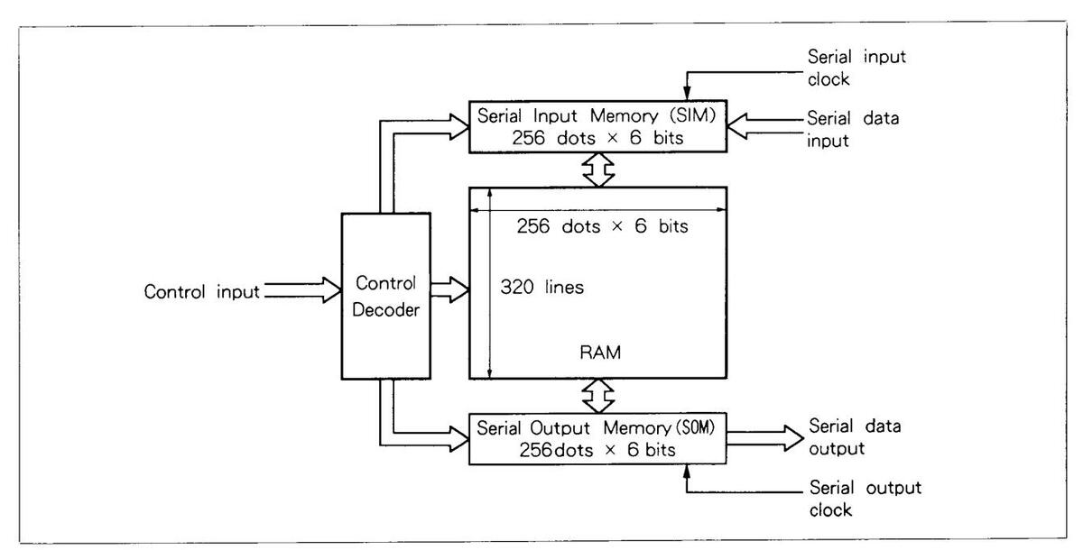
Fig. 3-47. Block Diagram of M5 M4 C500 AL Internals
Fig. 3-47. is a memory block diagram. Memory reading and writing are explained using this diagram.
Writing
Serial input memory stores serial input data (SID 1~6) in sync with the serial input clock (SIC). The stored data is transferred from SIM to RAM in accordance with the control input. At that time, the line of RAM to which to perform the transfer is controlled by specifying a line address via the control input.
• Reading
Lines to be read are transferred from RAM to SOM in accordance with the control input, and the data transferred to the SOM is output in sync with the serial output clock.
Memory space of 320 lines × 256 dots × 6 bits is available for both the intensity signal and the coloration signals. For NTSC mode, each field takes 106 lines, so the memory used is 3 fields × 106 lines × 256 dots × 6 bits, as follows.
Lines 0 ~ 105 : Field 1
Lines 106 ~ 211 : Field 2
Lines 212 ~ 317 : Field 3
Regardless of whether fields are odd or even, the order in which writing is performed is as follows.
Field 1 → Field 2 → Field 3 → Field 1
For PAL mode, each field takes 140 lines, so the memory used is 2 fields × 140 lines × 256 dots × 6 bits, as follows.
Lines 0 ~ 139 : Field 1 Lines 140 ~ 279 : Field 2
Regardless of whether fields are odd or even, the order in which writing is performed is as follows. Field 1 → Field 2 → Field 1
2 Display Mode
Reduction and enlargement of input signals is determined by WBGXSM, RBGXSM, and FLXQD in the I2C.
| 0 | ||||
|---|---|---|---|---|
| Mode 1 | Mode 2 | Mode 3 | Mode 4 | |
| WBGXSM | 0 | 1 | 1 | 1 |
| RBGXSM | 0 | 0 | 1 | 1 |
| FLXQD | 0 | 0 | 0 | 1 |
|
Reduction /
enlargement ratio Screen |
1 : 1/4 | 1:1 | 1 : 4 | 1:4 |
The following table shows the various setting values, along with their reduction and enlargement ratios.
When the quad adapter is performing quad display, mode 1, 2, or 3 can be freely chosen for each of the four gate arrays. Mode 4 is for performing zoom-up on just one screen when playing back a recorded VTR tape. An explanation of each mode is presented below.

«Vertical Control Method»
The number of lines stored into memory is 106, with one interval stored for each two lines. The line from which to start storage is specified by I2C register WSTV. When using the write vertical filter, set FILONW to "H" and set FILONR to "L". The function of the write vertical filter is to perform smoothing in the vertical direction by using line memory to delay the signal in its multiplexed state by 1 H, and then averaging it with the current signal.
Reading is performed based on HD and VD created by the external fixed crystal oscillator (oscillator frequency 19.982 MHz) connected to the gate array whose I2C main address is 2. These CLK, HD, and VD signals are supplied to all gate arrays via external connection. HD and VD have the same frequency and phase relationship as standard NTSC, so there are odd fields and even fields.
Determination of the field to read is dependant upon whether the currently written field and other fields are even or odd, and whether the field to read is even or odd. Reading is not performed on a field which is in the process of being written, so one of the other fields is read.
For example, if the read field is odd and the write field is field 2, and if field 1 is even and field 3 is odd, then
field 3, which has the same even/odd characteristic as the read field, is read in. If field 1 and field 3 had the same even/odd characteristic, then field 1, which
has the more recent data, would have been read in. The following table gives an overview of the various read fields.
| Read field | Field 1 | Field 2 | Field 3 | Field that is Read In |
|---|---|---|---|---|
| Odd | Odd | Odd | Write | Field 2 |
| Odd | Even | Write | Field 1 | |
| Even | Odd | Write | Field 2 | |
| Even | Even | Write | Field 2 | |
| Odd | Write | Odd | Field 1 | |
| Odd | Write | Even | Field 1 | |
| Even | Write | Odd | Field 3 | |
| Even | Write | Even | Field 1 | |
| Write | Odd | Odd | Field 3 | |
| Write | Odd | Even | Field 2 | |
| Write | Even | Odd | Field 3 | |
| Write | Even | Even | Field 3 | |
| Even | Odd | Odd | Write | Field 2 |
| Odd | Even | Write | Field 2 | |
| Even | Odd | Write | Field 1 | |
| Even | Even | Write | Field 2 | |
| Odd | Write | Odd | Field 1 | |
| Odd | Write | Even | Field 3 | |
| Even | Write | Odd | Field 1 | |
| Even | Write | Even | Field 1 | |
| Write | Odd | Odd | Field 3 | |
| Write | Odd | Even | Field 3 | |
| Write | Even | Odd | Field 2 | |
| Write | Even | Even | Field 3 |
By operating in the above manner, even with three fields' worth of memory, there are never situations such as self-destruction in which the read address overruns the write address (resulting in only one field being stored in memory) and changes in the vertical position of the read picture signal (resulting in only two fields being stored in memory).
The following is an uncomplicated description of write scan lines and read scan lines. For explanation purposes, a simple model with only 12 scan lines is employed.
| Ο | 1 | |
|---|---|---|
| ۲ | 2 | |
| Ο | 3 | Even field scan lines |
| 4 | ○ : Odd field scan lines | |
| Ο | 5 | |
| 6 | ||
| Ο | 7 | |
| 8 | ||
| Ο | 9 | Odd field write scan lines : 1, 5, and 9 |
| ۲ | 10 | Even field write scan lines : 2, 6, and 10 |
| Ο | 11 | |
| ۲ | 12 | |
Manner in which Scan Lines are Stored in Memory
| Ο | 1 | |
|---|---|---|
| 2 | ||
| Ο | 3 | |
| 4 | ||
| О | 5 | |
| 6 | ||
| О | 7 | |
| 8 | ||
| Ο | 9 | |
| 10 | ||
Display Method within Output Picture Signal
Operation usually proceeds as shown in the diagrams above, but when there are only even input signals or only odd input signals, operation proceeds as shown in the diagrams below.
| 0 1 | 02 |
|---|---|
| • 1 | • 6 |
| 05 | 06 |
| • 5 | • 10 |
| 09 | O 10 |
| • 9 | • 10 |
| Only Even Input | Only Odd Input |
In the above diagrams, when the read field is even
and an odd field is read, this starts at "6", and "10" is read twice. As will be described later, this is a method of dealing with the fact that in PAL mode there are only two fields' worth of memory.
«Horizontal Control Method»
Writing
The clock provided to the A/D converter from the gate array is 1270 fH in terms of the input picture signal, or approximately 20 MHz. This remains the same regardless of the mode. The Y signal, R-Y signal, and B-Y signal, which are multiplexed by the A/D converter, are input to the gate array. At that point, timing is reconciled, and the signals are input in their multiplexed state to the line memory. If the write vertical LPF is utilized, the multiplexed signal from this line memory, delayed by 1 H, is added with the signal currently being input to the gate array. If write vertical
LPF is not utilized, this summation processing is not performed. This is the only difference between the use and non-use of write vertical LPF. During memory writes, signals in their multiplexed state are input to both the intensity signal memory and the coloration signal memory. When the intensity signal is being input to the memory, the intensity signal memory's clock beats, and when the coloration signal memory's clock beats. Based on this type of clock operation, the separate writing of the intensity signal and the coloration signal is realized.
Additionally, by delaying the coloration memory's write clock, the delay in the coloration signal caused by the encoder prior to the A/D converter is compensated.
The block diagram for this segment is shown in fig. 3-48.
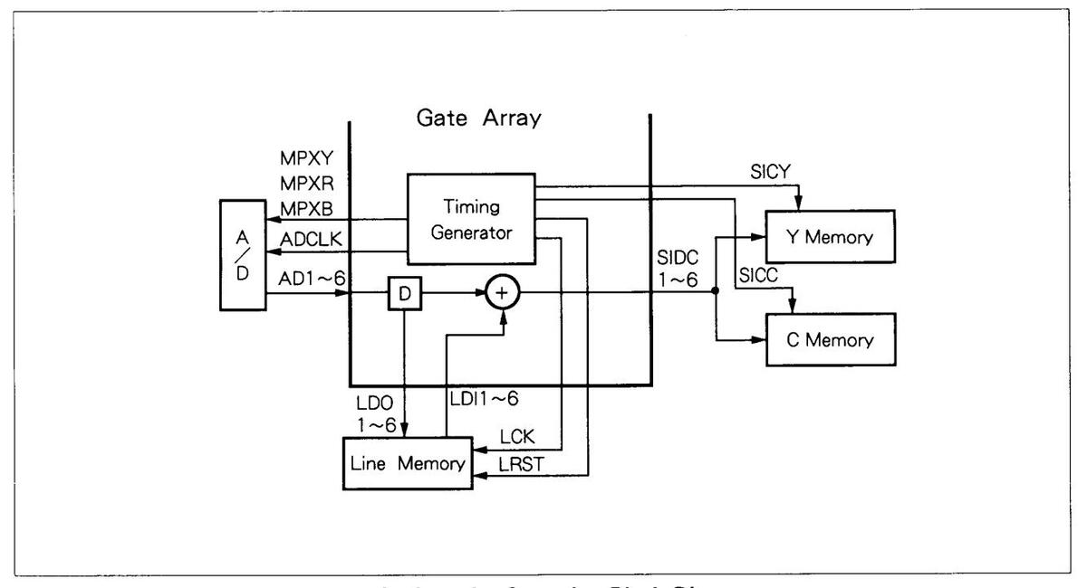
Fig. 3-48. Write Operation Block Diagram
Fig. 3-49. presents a timing chart for this segment. The sampling speed for the intensity signal is 5 MHz, and that for the coloration signals is 2.5 MHz. The multiplex method is :
Line memory utilizes an NEC µ PD 42101 and a shared read clock and write clock with a frequency of 10 MHz. In the time chart, Y1, R1, etc. are the signals currently being input from the A/D converter to the gate array; Y1', R1', etc. are the signals which
are output from the line memory and delayed by 1 H; and Y1", R1", etc. are the signals subsequent to the vertical LPF. Meanwhile, memory write clocks SICY and SICC carry out control functions by masking the 20 MHz master clock, and are set up to rise 256 times during each 1 H interval.
Although the SICY and SICC clocks rise 256 times for all scan lines, SIM to RAM memory transfers are not performed for scan lines to which writing is not desired. Thus, even if the SIM is written to, the RAM will not be, so no problems will arise.

Fig. 3-49. Write Operation Time Chart
Reading
As described earlier, read operations are carried out based on an external oscillator clock signal and the HD and VD signals created from it. The brightness signal memory and coloration signal memory each is provided with its own read clock, and the brightness signal and coloration signals are input to the gate array via separate pins as well. The frequency of the read clock is 10 MHz. Signals which are read out are multiplexed within the gate array and then input to the D/A converter. At that time, in order to prevent collisions with the output from another gate array, the
output pins of a gate array's multiplex signal are only enabled during the display interival, and at other times are placed in the high impedance state. During the blanking interval and border interval as well, by setting an I2C PAXCH signal to "H", only one of the four gate arrays is enabled and outputs a blanking level signal. For the D/A converter's clock signals, a Y clock, B-Y clock, and R-Y clock are output by the gate array whose I2C main address is 3.
The read vertical LPF is not necessary in this mode. A block diagram for this segment is presented in figure 3-50.

Fig. 3-50. Read Operation Block Diagram

Fig. 3-51. Read Operation Time Chart
CLKY is 10 MHz, while CLKR and CLKB are 5 MHz. The size of the data output from a gate array is 256 dots for the Y signal, and 128 dots for the R-Y and B-Y signals. Further, in order to compensate for the delay in the coloration signal in the encoder after the A/D converter, SOCC is in actuality even faster than WSOY.
«Picture Sensor»
In the PLL, during two consecutive H's of every V, a 6-dot-wide brightness signal pulse is generated, and the sum of the brightness signal values during this period is recorded. The difference between this total and the one from 2V earlier is calculated and compared with the picture sensor sensitivity GSF 6-0 which has been set in the l2C. If the brightness difference is the larger of the two, a change is considered to have occurred on the screen, and the GSEN output terminal goes high.
During the picture sensor interval, if GSON in the l2 C is high, then a marker is displayed. The brightness of this marker can be set via GSM 6-0 in the l2C. The pulse positions and block diagram for the picture sensor are presented in figures 3-52 and 3-53.
Fig. 3-52. Pulse Positions of Picture Sensor

Fig. 3-53. Picture Sensor Block Diagram
The sensitivity of the picture sensor is determined by picture sensor sensitivity setting GSM 6-0. Supposing, however, that this value were set to 12, then since there are 12 dots in the brightness signal during the sensor interval, a sensor alarm will be generated if the difference in digital values averages 1 or greater. A digital value of 1 corresponds to 0.78 IRE.

B-Y → 128 dots
In this manner, equivalently sized output of an arbitrary one-quarter-sized portion of an input picture signal can be performed in this mode.
«Vertical Control Method»
The control methods for read and write fields are the same as those for mode
| Ο | 1 | |
|---|---|---|
| ۲ | 2 | |
| Ο | 3 | |
| ۲ | 4 | Even field scan lines |
| Ο | 5 | O : Odd field scan lines |
| 6 | ||
| Ο | 7 | |
| 8 | Odd field write scan lines : 3, 5, and 7 | |
| Ο | 9 | Even field write scan lines : 4, 6, and 8 |
| ۲ | 10 | |
| 0 | 11 | |
| ۲ | 12 |
Manner in which Scan Lines are Stored in Memory
| О | 3 |
|---|---|
| 4 | |
| Ο | 5 |
| 6 | |
| О | 7 |
| 8 |
Display Method within Output Picture Signal
Operation usually proceeds as shown in the diagrams above, but when there are only even input signals or only odd input signals, operation proceeds as shown in the diagrams below.
«Horizontal Control Method»
• Writing
The block diagram is for the most part the same as that for mode 1, but there is no vertical LPF. This is because scan line thinning is not performed and there is thus no need for filter processing. Respective scanning frequencies are 10 MHz for Y, 5 MHz for R-Y, and 5 MHz for B-Y. In figure 3-54, only the time chart is presented.
Fig. 3-54. Write Operation Time Chart
Reading
Omitted since it is exactly the same as that for mode 1.
(Mode 3) Quad display with 1 : 4 enlargement/ reduction ratio WBGXSM = "1" RBGXSM = "1" FLXOD = "0"
The diagram below shows how the input picture signal is enlarged.

Y → 128 dots R-Y → 64 dots B-Y → 64 dots
This is a mode which takes 1/16 of an input signal, enlarges it by a factor of 4, and displays it as 1/4 of the output signal.
《Vertical Control Method》
Storage to memory is performed in the form of three fields of 106 lines. Reading is performed on the 53 lines of this. The allocation of memory space and the order in which writing is performed are the same as for modes 1 and 2, but the method in which read fields are selected is different. In this mode, regardless of whether the read and write fields are even or odd, the read field is the field immediately prior to the one on which a write is currently being performed. If, for example, the write field is field 2, the read field will be field 1, which was written before 1V. An overview of the read field is shown below.
| Write Field | Read Field |
|---|---|
| Field 1 | Field 3 |
| Field 2 | Field 1 |
| Field 3 | Field 2 |
The reason this was done is that, since reading is even slower than writing, if the field which is two before the one being written is read, there is the possibility of "self-destruction," in which a write to that field begins while the read is in progress and an address overrun occurs. This situation is illustrated in fig. 3-55.
Fig. 3-55. Situation where Address Overrun Occurs when Reading a Field 2V Back
The read field is selected based on either the field being written at the time that the read commences or, if a field is not being written, the last field to have been written previously. In the diagram above, a close look at the start time for the read of field 2 reveals that, at that point, the write of field 1 has finished and the write of field 2 has not begun, so field 1 is considered the field which is currently being written. As a result, field 2 - the field which is 2V back from
field 1, which is being written - is selected as the field to read. During this read, however, a write begins, resulting in the occurrence of an address overrun. If the field which is 1V back from the write field is read, this type of problem will not occur. This situation is illustrated in the diagram below.

Fig. 3-56. Reading a Field 1V Back
Write scan lines are the same as for mode 2. They are described one more time below.
| Ο | 1 | ||
|---|---|---|---|
| 2 | |||
| Ο | 3 | ||
| ļ | 4 | : Even field scan lines | |
| Ο | 5 | O : Odd field scan lines | |
| ( | 6 | ||
| ( | Ο | 7 | |
| ( | 8 | Odd field write scan lines : 3, 5, and 7 | |
| ( | Ο | 9 | Even field write scan lines : 4, 6, and 8 |
| ( | 10 | ||
| ( | Ο | 11 | |
| ( | 12 | ||
Manner in which Scan Lines are Stored in Memory
Read scan lines are considerably different from those in modes 1 and 2. Even if input picture signals have even/odd characteristics, a read field still cannot be selected. Thus, if the read field is odd, the field which is read might be odd or even. The diagram below shows scan line conditions for cases in which the even/odd characteristics of the read field and the field which is read match and cases in which they do not match.
| 03 | 04 | 04 |
|---|---|---|
| • 4 | • 5 | • 3 |
| 03 | 04 | 04 |
| • 4 | • 5 | • 3 |
| 05 | 06 | 06 |
| • 6 | • 7 | • 5 |
| 05 | 06 | 06 |
| • 6 | • 7 | • 5 |
| 07 | 08 | 08 |
| • 8 | • 7 | • 7 |
| 07 | 08 | 08 |
| • 8 | • 7 | • 7 |
| (a) Match | (b) Do not match | (c) Reference |
In the non-matching case, when there is an even field and an odd field is read, the read operation begins not with 3, but rather with the value that follows it : 5. This is to deal with the fact that if reading starts with 3, then the situation shown in (c) results, and the frequency of scan line reversals increases. Even so, scan line reversals still do occur, causing jagged diagonals to appear on the screen. The read vertical LPF is used to diminish this effect. As a result, if the read scan line changes when the read field is odd, then the average is taken between the line currently being read and the line which is 1H back. No processing takes places when the read field is even. The reason for this is that picture distortion occurs if too much processing is performed. The situation in which the read filter is utilized is as follows
《Horizontal Control Method》
Writing
Omitted since it is exactly the same as that for mode 2.
Reading
The brightness signal memory and coloration signal memory each is provided with its own read clock, and the brightness signal and coloration signals are input to the gate array via separate pins as well. The frequency of the read clock is 5 MHz. Signals which are read out are multiplexed within the gate array. When using the read vertical LPE, the signals are then input to the line memory where the line memory output which was delayed by 1H is averaged with the current input signal, and the resulting signal is then input to the D/A converter. When not using the read vertical LPF the multiplexed signals are input as is to the D/A converter. A block diagram and time chart for this segment are shown in fig. 3-57 and 3-58. To use the read vertical LPF, perform I2C settings FILONW = "L" and FILONR = "H"; when not using it, perform I2C settings FILONW = "L" and FILONR = "H". Line memory is shared with the write vertical LPF, but since there is never a need to turn on both the write vertical LPF and the read vertical LPF, this is not a problem.

Fig. 3-57. Read Operation Block Diagram
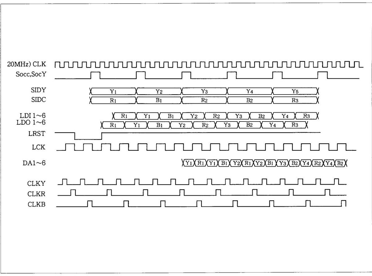
Fig. 3-57. Read Operation Time Chart
In the time chart in the previous diagram, there are differences in format between the line memory's multiplex signal and the multiplex signal which is input to the D/A converter. These differences are due to the fact that the line memory's multiplex signal includes summation processing and makes proper timing easier to achieve, while the multiplex signal which is input to the D/A converter has a format which is compatible with the gate array format which is output in other modes (modes 1 and 2). This is necessary since the D/A clock is output from a special gate array (whose I2C main address is "3").
(Mode 4) Full screen display with 1 : 1/4 enlargement/reduction ratio WBGXSM = "1" RBGXSM = "1" FLXQD = "0"
The diagram below shows how the input picture signal is enlarged.

Sampling count : Y → 256 dots R-Y → 128 dots B-Y → 128 dots
This is a mode which takes an arbitrary one-quarter region of the input signal, enlarges it by a factor of 4, and outputs it as the full output signal. The signal processing method is exactly the same as that for mode 3.
The difference is the fact that FLXQU on the l2C bus is set to high, and full screen output is performed.
The display modes which have been described thus far are brought together in the table shown below.
| Mode 1 | Mode 2 | Mode 3 | Mode 4 | ||
|---|---|---|---|---|---|
| Enlargement/reduction ratio | 1 : 1/4 | 1:1 | 1:4 | 1:4 | |
| Output display ra | ange | QUAD | QUAD | QUAD | FULL |
| Memory storage region |
51.2 μ sec
× (212/2) lines |
25.6 µ sec
× 106 lines |
12.8 µ sec
× 53 lines |
25.6 μ sec
× 106 lines |
|
| Υ | 256 dots | 256 dots | 128 dots | 256 dots | |
| Sampling count | R-Y | 128 dots | 128 dots | 64 dots | 128 dots |
| B-Y | 128 dots | 128 dots | 64 dots | 128 dots | |
| Comulia | Υ | 5 MHz | 10 MHz | 10 MHz | 10 MHz |
| frequency | R-Y | 2.5 MHz | 5 MHz | 5 MHz | 5 MHz |
| nequency | B-Y | 2.5 MHz | 5 MHz | 5 MHz | 5 MHz |
| Υ | 10 MHz | 10 MHz | 5 MHz | 5 MHz | |
| R-Y | 5 MHz | 5 MHz | 2.5 MHz | 2.5 MHz | |
| пециенсу | B-Y | 5 MHz | 5 MHz | 2.5 MHz | 2.5 MHz |
| Vertical filter | Write possible | Both impossible | Read possible | Read possible | |
Table. 3-9. Display Modes
③ Still Mode
• Frame Stills
When NSTILL is set to "H" in the I2C, then as soon as the gate array recognizes this setting, it will record the frame appearing immediately thereafter one line at a time alternately to field 1 and field 2, as shown in the diagram below. The gate array will, furthermore, prohibit writing after this recording is completed. When reading, field 1 is read for odd fields, and field 2 is read for even fields. Consequently, a still with a high vertical resolution results. This is only valid during the mode 1 reduction mode.
Even field scan lines Odd field scan lines
| Ο | 1 | Write to field 1 | O 1 |
|---|---|---|---|
| 2 | • 3 | ||
| Ο | 3 | Write to field 2 | 05 |
| 4 | • 7 | ||
| Ο | 5 | Write to field 1 | 09 |
| 6 | • 11 | ||
| Ο | 7 | Write to field 2 | |
| 8 | When reading : | ||
| Ο | 9 | Write to field 1 | Odd fields → field 1 |
| 10 | Even fields → field 2 | ||
| Ο | 11 | Write to field 2 | |
| 12 | |||
Write Scan Lines when Frame Still is Performed for an Odd Field
• Field Stills
This is a still mode which foregoes the operations performed for frame stills, and simply writes one field into one field's worth of memory. In this mode, any field from among fields 1, 2, and 3 can be freely selected for the write field and read field. This mode is entered when FSTILL is set to "H".
Writing is normally not performed when this mode is entered, but if, for example, overwriting of the contents of field 1 is desired, then when P1WR changes from "L" to "H" (it must be set to low once if it was initially high), field 1 will be overwritten with the frame which follows immediately thereafter. The same mechanism applies for field 2 and field 3 as well. For reading, set P1RD to "H" in order to read field 1, set P2RD to "H" in order to read field 2, or set P3RD to "H" in order to read field 3. If P1RD, P2RD, and P3RD are all set to "L", field 1 will be taken as the target of read operations.
The above descriptions are summarized in the table below.
| FSTILL | P1WR | P2WR | P3WR | P1RD | P2RD | P3RD | Write Field | Read Field |
|---|---|---|---|---|---|---|---|---|
| н | Unchanged | Unchanged | Unchanged | _ | — | — | None | |
| Н | Rising | Unchanged | Unchanged | _ | Field 1 | _ | ||
| Н | Unchanged | Rising | Unchanged | _ | _ | _ | Field 2 | _ |
| н | Unchanged | Unchanged | Rising | _ | - | Field 3 | _ | |
| Н | — | L | L | L | _ | Field 1 | ||
| Н | _ | - | Н | - | _ | _ | Field 1 | |
| Н | _ | L | Н | _ | _ | Field 2 | ||
| H | _ | L | L | н | _ | Field 3 | ||
| L | _ | - | _ | — | - | Normal operation | Normal operation |
Table. 3-10. Still Mode
These stills work in all modes.
3-3-4. Memory Circuit (VD1)
(1) Overview
This set utilizes the M5 M4 C5004 VP-5 IC as 320 × 256 × 6 field memory for holding three fields of a single quarter-screen section of a quad screen. For each of the four quarter-screens, one IC is used for each of Y and C, for a total of eight ICs. In addition, the µ PD 41101 1H line memory IC is utilized to hold horizontal lines during G.A4-only VCR playback zooms. The specifications for each type of memory are presented below.
1 Field Memory
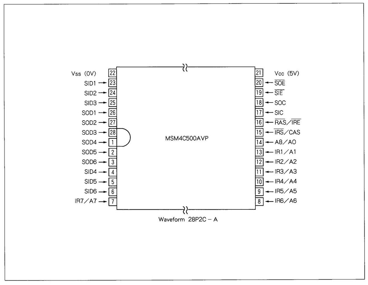
Fig. 3-59. Field Memory Pin Connection Diagram

Fig. 3-60. Field Memory Overall Block Diagram
• Overview
Capable of simultaneous, asynchronous operation or independent operation, this memory supports high speeds of up to 100 MHz. It offers a 256 × 6=1,536 bit serial input memory capable of serial input in 6 bit parallel, as well as a 256 × 6=1,536 bit serial output memory capable of serial output. In addition to these two serial memories, it is also equipped with a 320 × 256 × 6=491,520 bit dynamic RAM capable of 256 × 6=1,536 bit data transfers.
Using silicide technology based three-layer gates as well as CMOS process technology, this memory achieves a combination of high integration, high speed, and low power consumption.
The serial input memory and serial output memory are iointly addressable, with serial input or serial output possible from any column address. BAM is also addressable, with 256 × 6 bit data transfers possible between any RAM row address and the serial input memory or serial output memory. For RAM row address specification, two counters are built in (one for serial input and one for serial output) with six types of row address specification possible. Two types of column address specification for the serial input memory and serial output memory are also possible. To refresh the RAM memory, a refresh address counter is also built in, so refresh is possible without external address input. The refresh time for RAM memory cells, however, is a long 20 ms, so when used as video memory, memory cell refresh can be used as a substitute for video screen refresh.
In addition, by multiplexing and specifying row address, column address, and instruction codes representing various operations, it can be loaded into a 28-pin TSOP package, thus facilitating the high density packaging of application systems.
This memory can be used in TV and VTR applications, and if used as video signal field memory, it can accomplish a large variety of functions. This memory can be applied in NTSC, PAL, and SECAM formats.
Features
-
1. Row Access Memory (RAM)
- Dynamic memory comprised of 320 × 256 × 6= 491,520 bits
256 × 6 bit data transfers between SIM and RAM 256 × 6 bit data transfers between RAM and SOM
9-bit row address selection possible (1 of 320) Built-in address counter dedicated to RAM memory cell refresh
2. Serial Input Memory (SIM) High-speed serial input in 6-bit parallel possible Minimum cycle time 100 ns Dynamic memory comprised of 256 × 6=1,536 bits Address selector comprised of 256 bits 8-bit column address selection possible (1 of 256) Two types of column address setting possible -
Two types of column address setting possible - external address/0 address
3. Serial Output Memory (SOM)
High-speed serial output in 6-bit parallel possible Minimum cycle time 100ns Static data registers comprised of 256 × 6=1,536 bits Address selector comprised of 256 bits 8-bit column address selection possible (1 of 256) Two types of column address setting possible external address/0 address
4. Data Transfers between SIM and RAM
Bidirectional 256 × 6 bit data transfers between single rows of SIM and RAM Six types of RAM row address setting possible, including external address, 0 address, and internal address counter (Internal address counter is specifically for transfers between RAM and SIM)
- 5. Data Transfers between RAM and SOM Bidirectional 256 × 6 bit data transfers of between SOM and single rows of RAM Six types of RAM row address setting possible, including external address, 0 address, and internal address counter (Internal address counter is specifically for transfers between RAM and SOM)
- 6. SIM and SOM can perform data input and output in simultaneous, asynchronous fashion or in independent fashion
- Memory Refresh Time RAM: Max. 20ms/320 row addresses
- 8. Twin-well CMOS process technology
- 9. Input/output levels are TLL compatible
- 10. Single 5 V power supply
- 11.28-pin TSOP package
• Functional Description of Terminals
| Terminal Name | Name | 1/0 | Remarks |
|---|---|---|---|
| ĪRS/CAS |
Instruction strobe/
Column address strobe |
I | Clock for retrieving a 7-bit instruction code, the most significant bit of a row address, and an 8-bit column address on a rising edge. |
| RAS/IRE |
Row address strobe/
Instruction enable |
I | Clock for retrieving an 8-bit row address and terminating the execution of an instruction. This clock is also utilized as the enable for instruction execution. |
|
A8/A0
IR1/A1 IR2/A2 IR3/A3 IR4/A4 IR5/A5 IR6/A6 IR7/A7 |
Instruction code (IRi)
/Row address (Ai) /Column address (Ai) |
I | Inputs, in three steps, an instruction code, a row address, and a column address. In the first step, instruction code IR 1-IR 7 and most significant row address component A 8 are input on a rising edge of IRS/CAS. In the second step, A 0-A 7 of the row address is input on the falling edge of RAS/IRE. In the third step, column address A 0-A 7 is input on the rising edge of IRE/CAS. |
| SIC | Serial input clock | I |
Clock for serially writing 6-bit SIDi data to the serial input memory
(SIM). Data is retrieved on the rising edge of SIC. After data is written, advances SIM address upward. |
| SIE | Serial input enable | 1 | Allows writing of 6-bit SIDi data to the serial input memory (SIM). |
| SID1-SID6 |
Serial input data
(SIDi) |
1 | Serial input terminal for 6-bit data. |
| SOC | Serial output clock | I |
Clock for reading out one 6-bit word from the serial output
memory (SOM) to the SODi. Accesses the SOM on the rising edge of SOC. Output data is held until the next SOC rising edge. After data is read, advances SOM address upward. |
| SOE | Serial output enable | 1 | Allows the reading out of one 6-bit word from the serial output memory (SOM) to the SODi. |
| SID1-SID6 |
Serial input data
(SIDi) |
0 | Serial output terminal for 6-bit data. |
Table 3-11. Description of Field Memory Terminals
• Functional Overview
(Serial Data Input)
To input data from serial input port SID to serial input memory (SIM), first the address setting instruction SAI is used to write to SIM address selector SIM-AS, thus setting the starting column address.
Next, by inputting serial input clock SIC, the 6-bit contents of serial input data port SID 1-6 are written to one of the 256 words in the SIM data register SIM-DR which is specified by the contents of SIM-AS. After this data is written, the address is advanced by shifting the contents of SIM-AS upward by one bit. In turn, by inputting SIC, the contents of SID 1-6 can by written to SIM-DR for up to 256 words.
(Serial Data Output)
To output data to serial output port SOD from serial output memory (SOM), first the address setting instruction SAO is used to read from SOM address selector SOM-AS, thus setting the starting column address.
Next, by inputting serial output clock SOC, one of the 256 6-bit data words in the SOM data register SOM-DR which is specified by the contents of SOM-AS is read out to the 6-bit contents of serial output data port SOD 1-6.
After this data is read, the address is advanced by shifting the contents of SOM-AS upward by one bit. In turn, by inputting SOC, the contents of SOM-DR can be read out to SOD 1-6 for up to 256 words.
(SIM, SOM Column Address Setting)
To set the column address of serial input memory (SIM) address selector SIM-AS or serial output memory (SOM) address selector SOM-AS, either of two settings can be used: address setting by an external source or 0 address setting.
(WTI, RTI, and RTO)
For data transfers between serial input memory (SIM) and RAM, there is the write transfer instruction WTI to write, in one step, the 256 × 6 bit data contents of SIM-DR to the specified row address in RAM, and the read transfer instruction RTI to read out, in one step, the 256 × 6 bit data contents of the specified row address in RAM to SIM-DR. In addition, for data transfers between RAM and serial output memory (SOM), there is also the read transfer instruction is RTO to read out, in one step, the 256 × 6 bit data contents of the specified row address in RAM to the SOM data registers SOM-DR.
(Row Address Setting for WTI and RTI)
Setting the row address of RAM for transfer instructions between serial input memory (SIM) and RAM can be accomplished through the use of any one of several methods: address setting by an external
source, 0 address setting, built-in input row address counter IRC. Further, the next address can be placed the IRC after an instruction has been executed. For the address to place in the IRC, it is possible to select either the address used in the instruction or the incremented (+1) value. Accordingly, any of six methods for setting the RAM row address can be chosen.
(Row Address Setting for RTO)
Setting the row address of RAM for transfer instructions between serial output memory (SOM) and RAM can be accomplished through the use of any one of several methods: address setting by an external source, 0 address setting, built-in output row address counter ORC. Further, the next address can be input to the ORC after an instruction has been executed. For the address to place in the ORC, it is possible to select either the address used in the instruction or the incremented (+1) value. Accordingly, any of six methods for setting the RAM row address can be chosen.
The input row address counter IRC and the output row address counter ORC are separate counters, and each one can be used independently.
(RAM Refresh)
RAM memory uses dynamic memory cells. To hold the contents of these cells for longer than 20 ms, it is necessary to refresh the contents of RAM row addresses R 0 to R 319 within 20 ms. When refreshing the RAM, the built-in refresh counter is used to set the row address. Single rows are refreshed via RAM refresh instructions REF, SAI, and SAO. After executing these instructions, the contents of the refresh counter are automatically incremented (+1).
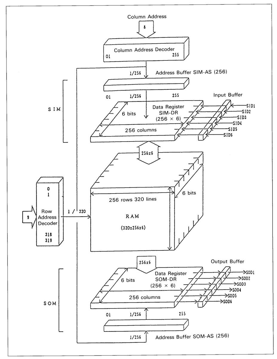
Fig. 3-61. Field Memory Block Diagram
2. 1H Line Memory
The µ D41101 is a high speed line-buffer for use in NTSC applications. It has a FIFO (first in first out) structure, and is comprised of 910 word × 8 bits. Using internal N-MOS dynamic circuits, the device achieves both high speed and low power consumption. By using the µ D41101, it is possible to easily implement one-line delays, time base conversions, and other operations related to TV and VTR systems.
In addition, with different cycles for reading and writing, the device can operate independently and asynchronously. This makes possible a wide variety of applications possible, including acting as a buffer for data transfers between devices with differing data processing speeds, or acting as a buffer for reconciling the synchronization of various input signals.
The µ D41101 is comprised of three types, depending on the cycle time.
Features
- 910 word × 8 bit configuration
- NTSC format : supports 4fsc sampling
- Asynchronous read/write operations possible
- Variable length delay bits (10 to 910bits) (for 8fsc)
- Power supply voltage of Vcc=5V ± 0%
- All input/output is TTL compatible
- 3-state outputs

Fig. 3-62. PD41101 Block Diagram
Absolute Maximum Ratings
| ltem | Symbol | Conditions | Rating | Units |
|---|---|---|---|---|
| Terminal voltage | VT | -1.5~+7.0 | V | |
| Power supply voltage | Vcc | -1.5~+7.0 | V | |
| Output current | lo | 20 | mA | |
| Operating temperature | Торт | -20~+70 | °C | |
| Storage temperature | T stg | -55~+125 | °C |
• Recommended Operating Conditions
| ltem | Symbol | Conditions | MIN. | TYP. | MAX. | Units |
|---|---|---|---|---|---|---|
| Power supply voltage | Vcc | 4.5 | 5.0 | 5.5 | V | |
| High level input voltage | V 1H | 2.4 | 5.5 | V | ||
| Low level input voltage | VIL | -1.5 | 0.8 | V | ||
| Surrounding temperature | Ta | -20 | +70 | °C |
٠
| ltem | Symbol | Conditions | MIN. | TYP. | MAX. | Units |
|---|---|---|---|---|---|---|
| Operating current | lcc | 90 | mA | |||
| Input leak current | I 1 | V 1 =0~V cc , other inputs 0V | -10 | 10 | mA | |
| Output leak current | lo | V 0 =0~5.5V, D OUT | -10 | 10 | mA | |
| High level output voltage | V он | I 0 = + mA | 2.4 | V | ||
| Low level output voltage | Vol | I 0 =2mA | 0.4 | V |
Input/Output Capacitance (Ta=25°C, f=1 MHz)
| ltem | Symbol | Conditions | MIN. | TYP. | MAX. | Units |
|---|---|---|---|---|---|---|
| Input capacitance | C 1 | 5 | рF | |||
| Output capacitance | Co | 7 | рF |
Basic Operation Timing
(1) Features of Input/Output Terminals
Data Input (D1N-07) Write data input. Data is latched on the rising edge after a WCK input cycle.
Set-up and hold times (tDST, tDH) are specified.
⊖ Data Output (DOUT 0-7)
Read data output. Access time is specified from the rising edge before an RCK input cycle, and defined to be tAC.
Reset Write Input (RSTW)
Reset input to initialize write address pointer. Reset signal is latched on the rising edge before a WCK input cycle. Set-up and hold times (tRS, tRH) are specified.
Reset Read Input (RSTR)
Reset input to initialize read address pointer. Reset signal is latched on the rising edge before a RCK input cycle. Set-up and hold times (tRS, tRH) are specified.
○Write Enable Input (WE)
Write operation control input. When disables ('H' level), internal write operations are prohibited, and the write address pointer is halted at the current position.
Read Enable Input (RE)
Read operation control input. When disables ('H' level), internal read operations are prohibited, and the read address pointer is halted at the current position. In addition, output goes into high-impedance state.
• Write Clock Input (WCK)
Write clock input. When WE is enabled ('L' level), write operations are performed in sync with the write clock. The write address pointer is also simultaneously incremented.
○ Read Clock Input (RCK)
Read clock input. When RE is enabled ('L' level), read operations are performed in sync with the read clock. The read address pointer is also simultaneously incremented.
(2) Operating Modes
Write Cycle
When WE input is enabled ('L' level), a write cycle is implemented in sync with the clock input.
The write cycle, in order to allow simple implementation of TV screen processing, input data is latched on the rising edge after the cycle so that processing of read and write data after l-line delay (910 bits) can be performed with the same clock. In addition, when creating a variable length delay line in the control of WE, the number of delay bits is 10 to 910 for 8fsc, and 5 to 910 for 4fsc.
Read Cycle
When RE input is enabled ('L' level), a read cycle is implemented in sync with the clock input, and data is output at time tAC (or tACR). In addition, when creating a variable length delay line in the control of RE, the number of delay bits is 10 to 910 for 8fsc, and 5 to 910 for 4fsc.
Further, when a read cycle and write cycle are competing for the same line during such operations as non-interlace conversion, old data (data from the previous line) may be output in the last 10 bits.
• Write Set Cycle, Read Reset Cycle
When power is turned on, the positions of the read address pointer and write address pointer are undefined. Consequently, these pointers must be initialized by first inputting the RSTR and RSTW signals.
The reset operation is possible at any time, and is set up to latch data on the first cycle (O address) after reset.
3-3-5. Oscillator Circuit (VD1)
This oscillator circuit features a built-in C-MOS IC and crystal oscillator in an extremely compact molded unit. This oscillator's frequency is used as the main clock for the gate arrays, and is the basis for read operations. Oscillation frequency is differs for NTSC and CCIR formats.
| NTSC 127 | Of 11 = 19.9825 MHz | |||
| PAL 127 | Of H = 19.8437 MHz | |||
| The voltage chara | cteristics of this oscillator are | |||
| presented below. | ||||
| Frequency | 19.9825 MHz | |||
| Power supply voltage | DC + 5 V ± 10 % | |||
| Current consumption 20 mA max. | ||||
| Output voltage | CMOS/TTL compatible | |||
| V 01 0.4 V and under | ||||
| V OH VDD - 0.5 V and under | ||||
| Load | N-TTL 10 (TTL), 15 pF (50 pF | |||
| max.) (CMOS) | ||||
| Frequency stability | ±100 ppm | |||
| Rise/fall time 5 nsec max. | ||||
| Duty cycle | 44-55% (at VDD/2) | |||
| 40-60% (at + 1.4 V) | ||||

7. ADJUSTMENTS
7-1. STANDARD SETTINGS
The signal and the power supply voltage during adjustment are shown below.
Power supply voltage : 120 V
Input signal : A step waveform produced by a 1 Vp-p reference video signal generator is input.
7-2. GATE ARRAY VCO ADJUSTMENT
| Adjustment location | Measurement location | Measurement Device | ||
|---|---|---|---|---|
| T2131 (PIP 1) TP213 (PIP 1) T2231 (PIP 2) TP223 (PIP 2) T2331 (PIP 3) TP233 (PIP 3) T2431 (PIP 4) TP243 (PIP 4) T2431 (PIP 4) TP115 (GND) | ||||
|
h. 1~ch. 4)
1 is performed by turning PIP4 are adjusted in the s |
g T2131 until TP213 | ||
7-3. DECODER VCXO ADJUSTMENT
| Adjustment location | Measurement location | Measurement Device | |||
|---|---|---|---|---|---|
| VC111 (DEC 1) TP114 (DEC 1) VC121 (DEC 2) TP124 (DEC 2) VC131 (DEC 3) TP134 (DEC 3) VC141 (DEC 4) TP115 (GND) | Frequency counter | ||||
|
C1 is performed by turning
Iz (NTSC) or 4433619± I DEC4 are adjusted in th |
g VC111 until TP114
10 Hz (PAL). le same manner. 279 nsec (NTSC) 225 nsec (PAL) |
|||
7-4. ENCODER VCXO ADJUSTMENT
| Adjustment location | Measurement location | Measurement Device | |||
|---|---|---|---|---|---|
| VC161 |
TP114,
TP115(GND) |
Frequency counter | |||
|
A IN 1 to the QUAD ONLY
VC161 until TP114 is 3 19 ± 10 Hz (PAL). |
OUT terminal.
2579545 ± 10 Hz |
|||
7-5. BRIGHTNESS AND BURST LEVEL ADJUSTMENT
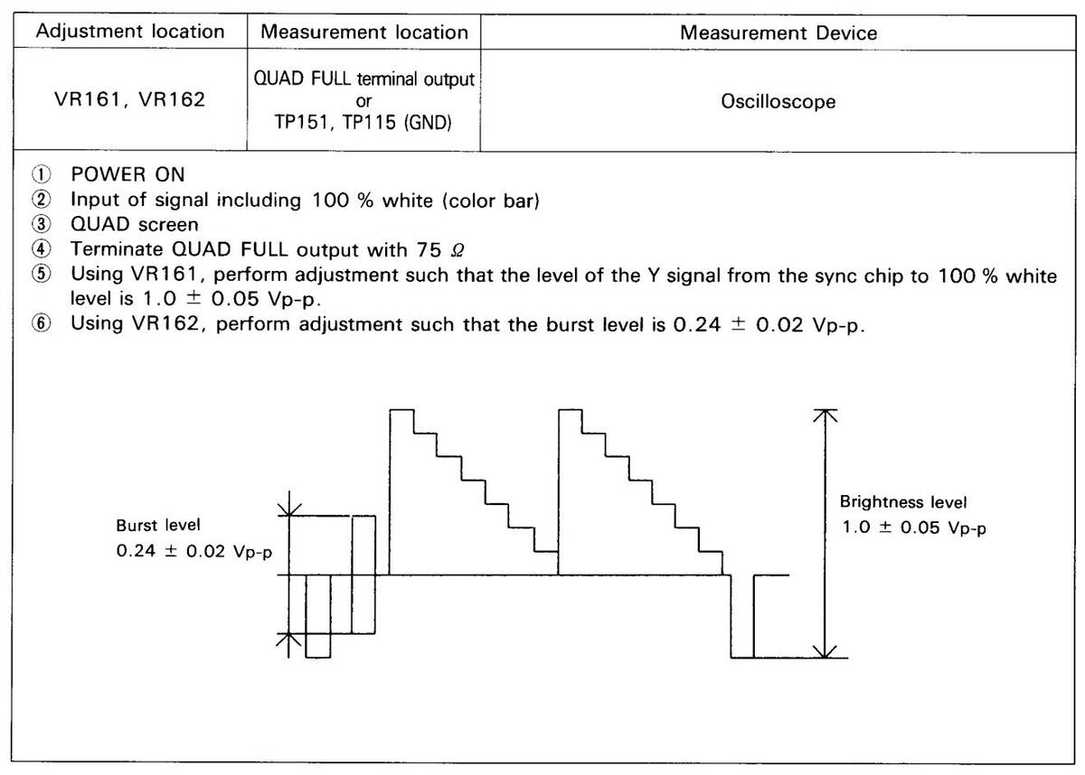
7-6. TINT ADJUSTMENT
7-6-1. TINT ADJUSTMENT (NTSC)
| Adjustment location | Measurement location | Measurement Device |
|---|---|---|
|
VR112 (DEC 1)
VR122 (DEC 2) VR132 (DEC 3) VR142 (DEC 4) |
QUAD FULL terminal output | Vector scope |
|
CAMERA IN 1 to 4
JLL output to a vector sc by adjusting the gain on th the tint, and adjust such all have the same inclina ner brackets. |
ope.
he vector that the tion and V. C. |
7-6-2. TINT ADJUSTMENT (PAL)
| Adjustment location | Measurement location | Measurement Device |
|---|---|---|
|
VR112 (DEC 1)
VR122 (DEC 2) VR132 (DEC 3) VR142 (DEC 4) |
TP112 (DEC 1)
TP122 (DEC 2) TP132 (DEC 3) TP142 (DEC 4) TP115 (GND) |
Oscilloscope,
Monitor |
|
CAMERA IN 1 to 4
JLL output to a vector so ariable resistor for each d waveform is singular and in flicker on the screen. |
cope and monitor.
ecoder (DEC), adjust d does not double. |
7-7. CHARACTER WIDTH ADJUSTMENT 1 (FULL)
| Adjustment location | Measurement location Mea | surement Device | |||
|---|---|---|---|---|---|
| VC181 | QUAD FULL terminal output | N | lonitor | ||
|
signal with recognizable m | onoscope pattern or | Center | ||
|
|
MENU 1 | |||
7-8. CHARACTER WIDTH ADJUSTMENT 2 (QUAD)
| Adjustment location | Measurement location | Measurement Device | |||
|---|---|---|---|---|---|
| VC182 | QUAD FULL terminal output | Monito | ər | ||
|
ch that the center line is i
J 3. |
n the space between
OFF C OFF C |
MEN
:AM 1 :AM 3 |
U 3
OFF CAM 2 OFF CAM 4 |
|
7-9. BIT-DROP CHECK
| Adjustment location | Measurement location | Measurement Device | |
|---|---|---|---|
| QUAD FULL terminal output | Monitor | ||
|
rideo signal input (Camera
of a quad screen, approx is, if there are 31 (distingu erter, gate array, and me rring in all four cameras, |
as 1 to 4 together)
imately 63 (practically indistinguishable) vertical lines can be uishable) lines, bit-drop is occurring; check the corresponding mory. the D/A converter is malfunctioning and must be checked. |
|
| 32 lines; LSB abnormal | |||
7-10.V. ADJ CHECK

7-11. IMAGE SENSOR CHECK
| Adjustment location Measurement location Measurement Device | ce | ||||
|---|---|---|---|---|---|
| QUAD FULL terminal output | Cam |
Monitor
era signal inpu |
ıt | ||
|
all sensors on via MENU
to each camera input and the sensor activates and e larm cancellation is perfor OOM, STILL, and MENU |
3.)
project the image. If ensures that the alarm rmed by pressing any keys). |
1
3 |
2 4 | |
7-12. ALARM IN/OUT CHECK
| Adjustment location | Measurement location | Measurement Device |
|---|---|---|
|
ALARM IN 1~8
(DIN-SUB 1~8 PIN) and GND (9 PIN), ALARM OUT (14 PIN) |
QUAD FULL terminal output | |
|
gnals to CAMERA IN 1 to
tch between GND (pin 9) JB pins 1 to 8).(CONTRO me the push switch corre een corresponding to the reen display. g that alarm, ALARM OU |
b 8.
and each of ALARM DL connector) sponding to an alarm number of that alarm JT (pin 14) is a low 1 |
7-13.SW. IN CHECK
| Adjustment location | Measurement location | Measurement Device |
|---|---|---|
|
SW. IN input
(DIN-SUB pin 12) and GND (pin 13) |
QUAD FULL terminal output | Monitor |
|
E of camera 1 to "EXT" in
er than MENU screen. gnals to CAMERA IN 1 to DIN-SUB pin 12) and GN n. (CONTROL connector) me the switch is pressed e camera on the screen s |
the MENU 2 screen.
o 8. ND (DIN-SUB pin 13) (each time there is a switches. 1 |
7-14. CLEARING THE E2PROM
| Adjustment location | Measurement location | Measurement Device | ||
|---|---|---|---|---|
| MENU KEY | Monitor | |||
|
ENU key and turn on the
creen appears, turn off th E 2 PROM memory. |
e power switch.
ne power switch. Ship |
2 4 | |
7-15.TP, VR, VC Locations

For U.S.A. only For parts or service contact

SFS Corporation: 1200 West Artesia Blvd., Compton, California 90220

-
SANYO Electric Co.,Ltd. Osaka, Japan
Sep./'93/1400/MI Printed in Japan


 Loading...