

Page 1
Ordering number : EN*6145
30499RM (OT) No. 6145-1/10
Overview
The SANYO LV2151V is a 2.0 GHz PLL frequency
synthesizer IC that features low-voltage operation and low
current drain and is suitable for CATV, DAB, and mobile
phone systems.
Features
• A wide range of operating frequency from 0.2 to
2.0 GHz
•I2C bus/ 3-wire bus selective. (For I2C bus WRITE
mode only)
• Includes three ports for band switch
• Includes unlock detect indicator.
• Battery saving mode
• 2.7V to 3.5 V operation
• Small package 20-pin SSOP ( Lead pitch 0.65mm)
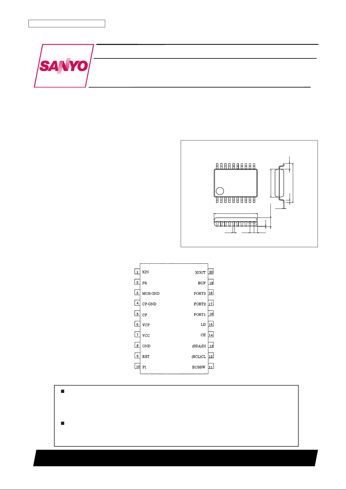
Package Dimensions
unit: mm
3179A-SSOP20
110
11
6.4
6.7
0.5
4.4
0.1
1.6max
1.0
20
0.650.22 0.43
0.15
Preliminary
SANYO: SSOP20
[LV2151V]
LV2151V
SANYO Electric Co.,Ltd. Semiconductor Bussiness Headquarters
TOKYO OFFICE Tokyo Bldg., 1-10, 1 Chome, Ueno, Taito-ku, TOKYO, 110-8534 JAPAN
2.0 GHz PLL Frequency Synthesizer IC
Bi-CMOS IC
Any and all SANYO products described or contained herein do not have specifications that can handle
applications that require extremely high levels of reliability, such as life-support systems, aircraft’s
control systems, or other applications whose failure can be reasonably expected to result in serious
physical and/or material damage. Consult with your SANYO representative nearest you before using
any SANYO products described or contained herein in such applications.
SANYO assumes no responsibility for equipment failures that result from using products at values that
exceed, even momentarily, rated values (such as maximum ratings, operating condition ranges, or other
parameters) listed in products specifications of any and all SANYO products described or contained
herein.
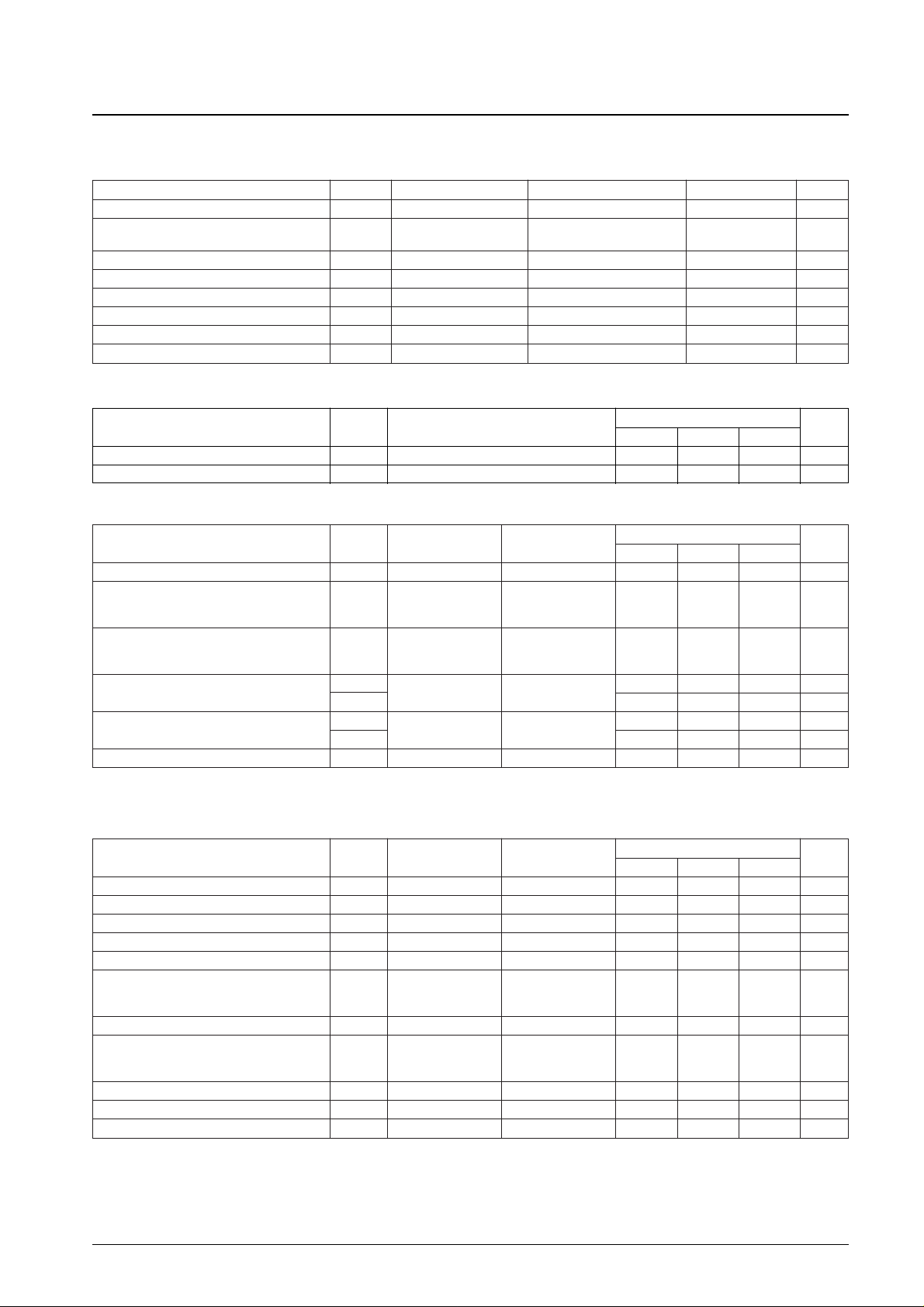
Pin Assignment
Page 2
No. 6145-2/10
LV2151V
Parameter Symbol Pin
Ratings
Unit
min typ max
Recommended power supply voltage V
CCVCC
, VCP 3.0 V
Operating voltage range V
CCOPVCC
, VCP 2.7 3.5 V
Operating Conditions at Ta = 25°C
Parameter Symbol Pin Conditions
Ratings
Unit
min typ max
Supply voltage V
CCVCC
, VCP 2.7 3.5 V
SCL(CL), SDA(DI),
High-level input voltage V
IH
CE, PS, RST, VCC*0.7 V
CC
V
BUSSW
SCL(CL), SDA(DI),
Low-level input voltage V
IL
CE, PS, RST, 0 0.6 V
BUSSW
Input frequency fin(1) XIN AC Coupled 4 22 MHz
fin(2) PI * 0.2 2.0 GHz
Input amplitude Vin(1) XIN AC Coupled –12 10 dBm
Vin(2) PI * –12 0 dBm
Guaranteed crystal oscillation Xtal XIN, XOUT 4 22 MHz
Allowable Operating Ranges at Ta = –30 to +85°C
Note: *50 Ω terminate (0 dBm = 0.224 Vrms)
Parameter Symbol Pin Conditions
Ratings
Unit
min typ max
Low-level output voltage1 V
O
L1 LD IO= 0.5 mA 0.4 V
Low-level output voltage2 V
O
L2 SDA(DI), PORT1 to 3 IO= 3.0 mA 0.4 V
Output off leak current I OFF LD, PORT1 to 3 V
O
= 3.0 V 1 µA
CP Output off leak current I OFCP CP V
O
= 1.5 V 100 nA
CP output current Icp CP V
O
= 1.5 V ±6.5 mA
SCL(CL), SDA(DI),
High-level input current1 IH1 CE, PS, RST, Vi = 3.0 V 5 µA
BUSSW
High-level input current2 IH2 XIN 3 µA
SCL(CL), SDA(DI),
Low-level input current1 IL1 CE, PS, RST, Vi = 0 V 5 µA
BUSSW
Low-level input current2 IL2 XIN 3 µA
Supply current Icco V
CC
+ VCP *1 7.0 mA
Standby current Isb No signal input Power saving mode 0.4 mA
Electrical Characteristics at Ta = 25°C, VCC= 3.0 V
Note: *PI = 2000 MHz, Vpi = 0 dBm, RI = 19.2 MHz, Vri = 0 dBm
Other input pins = 0 V, I/O pins = open, CP off, output pins = high
Parameter Symbol Pin Conditions Ratings Unit
Maximum supply voltage V
CC
max VCC, VCP 4.5 V
Maximum input voltage Vin max
SCL(CL), SDA(DI)
–0.3 to V
CC
+ 0.3 V
CE, PS, RST, BUSSW
Maximum output voltage Vout max LD, PORT1 to 3, SDA(DI) –0.3 to V
CC
+ 0.3 V
Maximum output current1 I
OUT
max1 PORT1 to 3, SDA(DI) 4 mA
Maximum output current2 I
OUT
max2 LD 0.7 mA
Allowable power dissipation Pd max Ta ≤ 85°C 50 mW
Operating temperature Topr –30 to +85 °C
Storage temperature Tstg –50 to +125 °C
Specifications
Absolute Maximum Ratings at Ta = 25°C
Page 3
No. 6145-3/10
LV2151V
Pin Descriptions
Pin Symbol I/O Description
1 XIN
CMOS input Crystal oscillator connection pins.
20 XOUT
Power saving switch.
2 PS CMOS input with a pull-down resistor built in. “Open or Low”: Power saving mode
“High”: Active mode
3 V
SS
Ground pin for logic system
4 CP-GND Ground pin for charge pump. (Fixed current output)
5 CP BIP output Charge pump output. (Fixed current output)
6 VCP V
CC
supply for charge pump.
7 V
CC
VCCsupply. (Except charge pump circuit)
8 GND Ground pin for RF block.
Reset pin for I
2
C bus.
9 RST CMOS input with a pull-up resistor built in.
Connect capacitor to GND.
“Open or High” Release
“Low” Reset
10 PI Bipolar input Comparator signal input. VCO output must be AC coupled to input.
Serial data select input.
11 BUSSW CMOS input with a pull-up resistor built in. “Open or High” I
2
C bus
“Low” 3-wire bus
12 SCL(CL) Data input pins
13 SDA(DI) CMOS input
14 CE CE is used as an address selector pin if I
2
C bus is used.
15 LD PLL unlock detector output pin.
16 PORT1
17 PORT2
NPN transistor open collector output
Output port pins for band switch.
18 PORT3
19 BUF Bipolar output Buffer output pin for crystal oscillator.
Page 4

Data Format
(1) 3-Wire Bus (BUSSW pin set low.)
1. Programmable Counter and Test Mode
ADD latch address data must be set to 1.
2. Reference Counter and Other Control
ADD latch address data must be set to 0
Serial Data Timing
No. 6145-4/10
LV2151V
t1, t2, t3, t4, t5 ≥ 100 ns
Page 5

(2) I2C bus BUSSW pin set open or high.
Address Byte
CE pin is high when the data is set to 1.
CE pin is low when the data is set to 0.
1. Programmable Counter and Testing Mode
2. Reference Counter and Other Control
Receiving Data Diagrams
No. 6145-5/10
LV2151V
Page 6

Serial Data Description
(1) Programmable Counter and Test Mode
Bit “ADD(Latch Address Data)” = 1
1. Programmable Counter
Bits P0 to P16 determine programmable divider ratios. Binary value with P0 as the LSB.
The division ratio can be set in the range of 4032 to 131071.
Ex. Settable division ratio factor is 8192
2. Test Mode
TS0 and TS1 are testing bits. These bits must normally be set to 0.
(2) Reference Counter and Other Control
ADD is the latch address bit. This bit must be set to 0.
1. Reference Counter
Bits R0 to R11 determine programmable divider ratios. Binary value with R0 as the LSB.
The division ratio can be set in the range of 20 to 4095.
Ex. Settable division ratio factor is 2048 (“*” = Don’t care)
2. Phase Comparator Output Control
Bit CPD is phase comparator polarity switching data.
Fig.1
3. Unlock Detection Control
ULD is used to control the signal length which determines whether or not the PLL is locked. PLL is determined as
unlocked if a phase error signal longer than that in the table below is detected.
No. 6145-6/10
LV2151V
CPD Phase comparator polarity
0 (1) Shown Fig.1
1 (2) Shown Fig.1
ULD Thresholds fXIN = 10.24 MHz
0 ±4/fXIN 390 ns
1 ±8/fXIN 780 ns
1 0 0 0 0 0 1 0 0 0 0 0 0 0 0 0 0 0 0 0
0 * * * * * * * 1 0 0 0 0 0 0 0 0 0 0 0
Page 7

4. Unlock Output Signal Extension Control
UE0 and UE1 are used to control the extension of LD signal detected in the unlock detector circuit.
5. Band Switching Output Ports
PORT1 to PORT3 are used to switch the outputs for pin16 to pin18, respectively. The pins go to high when the data
is set to 0, and go to low when set to 1.
No. 6145-7/10
LV2151V
UE1 UE0 Extension Time fref = 50 k
0 0 4*(1/fref) 80 µs
0 1 8*(1/fref) 160 µs
1 0 16*(1/fref) 320 µs
1 1 32*(1/fref) 640 µs
PORT* Output
0 High
1 Low
Page 8

LV2151V Evaluation Circuit
Unit (resistance: Ω, capacitance:F)
No. 6145-8/10
LV2151V
0.1 µ
V
VCO
0.1 µ
Page 9

Block Diagram
No. 6145-9/10
LV2151V
Page 10

PS No. 6145-10/10
LV2151V
This catalog provides information as of March, 1999. Specifications and information herein are subject to
change without notice.
Specifications of any and all SANYO products described or contained herein stipulate the performance,
characteristics, and functions of the described products in the independent state, and are not guarantees
of the performance, characteristics, and functions of the described products as mounted in the customer’s
products or equipment. To verify symptoms and states that cannot be evaluated in an independent device,
the customer should always evaluate and test devices mounted in the customer’s products or equipment.
SANYO Electric Co., Ltd. strives to supply high-quality high-reliability products. However, any and all
semiconductor products fail with some probability. It is possible that these probabilistic failures could
give rise to accidents or events that could endanger human lives, that could give rise to smoke or fire,
or that could cause damage to other property. When designing equipment, adopt safety measures so
that these kinds of accidents or events cannot occur. Such measures include but are not limited to protective
circuits and error prevention circuits for safe design, redundant design, and structural design.
In the event that any or all SANYO products (including technical data, services) described or contained
herein are controlled under any of applicable local export control laws and regulations, such products must
not be exported without obtaining the export license from the authorities concerned in accordance with the
above law.
No part of this publication may be reproduced or transmitted in any form or by any means, electronic or
mechanical, including photocopying and recording, or any information storage or retrieval system,
or otherwise, without the prior written permission of SANYO Electric Co., Ltd.
Any and all information described or contained herein are subject to change without notice due to
product/technology improvement, etc. When designing equipment, refer to the “Delivery Specification”
for the SANYO product that you intend to use.
Information (including circuit diagrams and circuit parameters) herein is for example only; it is not
guaranteed for volume production. SANYO believes information herein is accurate and reliable, but
no guarantees are made or implied regarding its use or any infringements of intellectual property rights
or other rights of third parties.
 Loading...