

SANYO LV1110NM Datasheet
Ordering number : EN6094
N2598RM (OT) No. 6094-1/22
Overview
The LV1110NM is a digital surround processor IC
developed for miniature stereo components and radiocassette combinations. The major features built into this
Bi-CMOS single-chip solution are function switching,
recording volume control, surround processing, karaoke
processing, 3-band graphic equalizer, and master volume
control.
Features
• The built-in delay functions include input and output
filters, analog-to-digital and digital-to-analog converters,
delay lines with built-in memory, and delay
reverberation. Other functions available are fixed matrix
(L+R and L-R) and front mixing (choice of level or
phase). These functions may be freely combined to
easily produce a variety of surround modes and thus
simulate a wide range of acoustic environments.
• The built-in karaoke functions include a vocal canceler,
microphone echo, key control I/O, and other support for
audio multiplexing software.
Functions
• Input function switching (Five channels with built-in
6-dB amplifier)
• Two REC output pins with volume controls (Two
channels with on/off switches and choice of function
output or mixer output)
• Input switching (choice of L+R, L–R, and L or R only)
• Microphone input (on/off)
• Vocal canceler
• Key control I/O pins
• Front addition (+3 dB, –3 dB, –5 dB, mute)
• I/O filters in delay block (choice of 2-, 5-, and 28-kHz
low pass filters or through operation)
• Reverberation functions (with built-in volume control)
• Built-in SRAM (8 kilobytes)
• Variable delay (choice of 15, 20, 25, 30, 40, 50, 100,
and 120 ms)
• Built-in V
DD
• I/O through or mute
• Three-band graphic equalizer (boost or cut with three
steps each)
• Master volume control from 0 to –79 dB in 1-dB steps
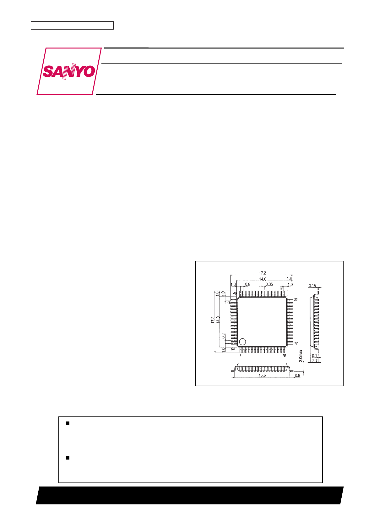
• QIP-64E package with 0.8-mm pin pitch
Package Dimensions
unit: mm
3159-QFP64E
SANYO: QFP64E (QIP64E)
[LV1110M]
LV1110NM
SANYO Electric Co.,Ltd. Semiconductor Bussiness Headquarters
TOKYO OFFICE Tokyo Bldg., 1-10, 1 Chome, Ueno, Taito-ku, TOKYO, 110-8534 JAPAN
Digital Surround Processor IC
Bi-CMOS IC
Any and all SANYO products described or contained herein do not have specifications that can handle
applications that require extremely high levels of reliability, such as life-support systems, aircraft’s
control systems, or other applications whose failure can be reasonably expected to result in serious
physical and/or material damage. Consult with your SANYO representative nearest you before using
any SANYO products described or contained herein in such applications.
SANYO assumes no responsibility for equipment failures that result from using products at values that
exceed, even momentarily, rated values (such as maximum ratings, operating condition ranges, or other
parameters) listed in products specifications of any and all SANYO products described or contained
herein.
No. 6094-2/22
LV1110NM
Parameter Symbol Conditions Ratings Unit
Maximum power supply voltage V
CC
max 12 V
Maximum power dissipation Pd max
Ta ≤ 70°C
500 mW
114.3 × 76.1 × 1.6 mm3Mounted on glass epoxy circuit board
Operating temperature Topr –25 to +70 °C
Storage temperature Tstg –40 to +125 °C
Specifications
Absolute Maximum Ratings at Ta = 25°C
Parameter Symbol Conditions Ratings Unit
Recommended power supply voltage V
CC
9 V
Operating power supply voltage range V
CC
opg 8 to 11 V
Control data high-level voltage V
IH
3.5 to 5.5 V
Comtrol data low-level voltage V
IL
0 to 1.2 V
Operating Conditions at Ta = 25°C
Parameter Symbol Conditions
Ratings
Unit
min typ max
Qurescent current I
CCO
19 28 42 mA
Input function switching (measured for function in input / function out)
Output level deviation
VG
F
1 IN A, D –2 0 +2 dB
VG
F
2 IN B, C, E 4 6 8 dB
Maximum output voltage V
OFVCC
= 8.5 V, THD = 1% 2.0 2.4 V
Distortion THD
F
400 to 30 kHz BPF 0.005 0.03 %
Output noise voltage V
NOF
Rg = 10 kΩ, JISA –102 –95 dBV
Interchannel crosstalk CT
F
Rg = 10 kΩ/VO= 1 Vrms, JIS A 82 100 dB
L and R channel total throughput (measured for L and R inputs and L and R outputs)
Output level deviation VG
T
–2 0 +2 dB
Signal handling SH
TVCC
= 8.5 V, THD = 1%, 300 mVrms = 0 dB 15.0 16.5 dB
Distortion THD
T
400 to 30 kHz BPF 0.005 0.03 %
Signal-to-noise ratio SNT Rg = 10 kΩ, CCIR-ARM, 300 mVrms = 0 dB 85 100 dB
Interchannel crosstalk CT
T
Rg = 10 kΩ/VO= 1 Vrms, JIS A 82 94 dB
S channel (measured for delay = 20 ms, reverb. off, L-R, S-IN input, S-OUT output)
Output level deviation VG
S
–3 0 +3 dB
Signal handling SH
S
THD = 3%, 300 mVrms = 0 dB, VCC= 8.5 V 15.0 16.5 dB
Distortion THD
S
400 to 30 kHz BPF, OUT FILTER: 5 kHz LPF 0.1 0.7 %
Signal-to-noise ratio SN
S
Rg = 10 kΩ, CCIR-ARM, 300 mVrms = 0 dB
60 68 dB
OUT FILTER: 5 kHz LPF
Long delay (measured for delay = 100 ms, reverb. off, MIC-IN input, S-OUT output)
Output level deviation VG
D
OUT FILTER: 2 kHz LPF –4.5 –1.5 +1.5 dB
Maximum output voltage V
OD
THD = 3%, VCC= 8.5 V 1.4 1.8 V
Distortion THD
D
400 to 30 kHz BPF, OUT FILTER: 2 kHz LPF 2.0 3.0 %
Output noise voltage V
NOD
Rg = 10 kΩ, JIS A, OUT FILTER: 2 kHz LPF –75 –66 dBV
Vocal cut VC –16 –20 –24 dB
[REC output (measured for volume = 0 dB, function in, A input, REC OUT)]
Output level deviation VG
R
–2 0 +2 dB
Maximum output voltage V
OR
THD = 1%, VCC= 8.5 V 1.6 2.0 V
Distortion THD
R
400 to 30 kHz BPF 0.006 0.03 %
Output noise voltage V
NOR
Rg = 10 kΩ, JIS A –106 –95 dBV
Interchannel crosstalk CT
R
Rg = 10 kΩ/VO= 1 Vrms, JIS A 82 100 dB
Mute attenuation ratio MT
R
JIS A, VIN= 1 Vrms = 0 dB –75 –86 dB
Electrical Characteristics at Ta = 25°C, VCC= 9 V, fIN= 1 kHz, VIN= 300 mVrms = 0 dB, RL= 10 kΩ
Continued on next page.
No. 6094-3/22
LV1110NM
Continued from preceding page.
Parameter Symbol Conditions
Ratings
Unit
min typ max
Master volume control (measured for volume = maximum, VOL IN input, VOL OUT output)
Output level deviation VG
V
–2 0 +2 dB
Maximum output voltage V
OVVCC
= 8.5 V, THD = 1% 1.6 2.0 V
Distortion THD
V
400 to 30 kHz BPF 0.006 0.03 %
Output noise voltage V
NOV
Rg = 10 kΩ, JIS A –107 –95 dBV
Interchannel crosstalk CT
V
Rg = 10 kΩ/VO= 1 Vrms = 0 dB, JIS A 85 103 dB
Mute attenuation ratio MT
V
JIS A, VIN= 300 mV = 0 dB –70 –78 dB
Graphic equalizer (measured for IN,L,R input / OUT L,R )
VGE
U
1
BASS: f
IN
= 100 Hz, MID: fIN= 1 kHz,
1.7 3 4.3 dB
TREBLE: BOOST1: f
IN
= 10 kHz
Boost amount VGE
U
2
BASS: f
IN
= 100 Hz, MID: fIN= 1 kHz,
4.7 6 7.3 dB
TREBLE: BOOST2: f
IN
= 10 kHz
VGE
U
3
BASS: f
IN
= 100 Hz, MID: fIN= 1 kHz,
8.5 10 11.5 dB
TREBLE: BOOST3: f
IN
= 10 kHz
VGE
D
1
BASS: f
IN
= 100 Hz, MID: fIN= 1 kHz,
–4.3 –3 –1.7 dB
TREBLE: CUT1: f
IN
= 10 kHz
Cut amount VGE
D
2
BASS: f
IN
= 100 Hz, MID: fIN= 1 kHz,
–7.3 –6 –4.7 dB
TREBLE: CUT2: f
IN
= 10 kHz
VGE
D
3
BASS: f
IN
= 100 Hz, MID: fIN= 1 kHz,
–11.5 –10 –8.5 dB
TREBLE: CUT3: f
IN
= 10 kHz
Electrical Characteristics at Ta = 25°C, VCC= 9 V, fIN= 1 kHz, VIN= 300 mVrms = 0 dB, RL= 10 kΩ
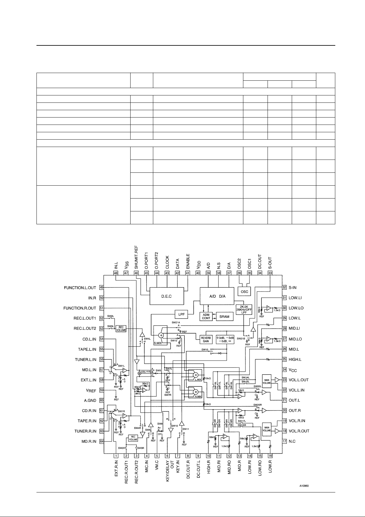
Block Diagram

No. 6094-4/22
LV1110NM
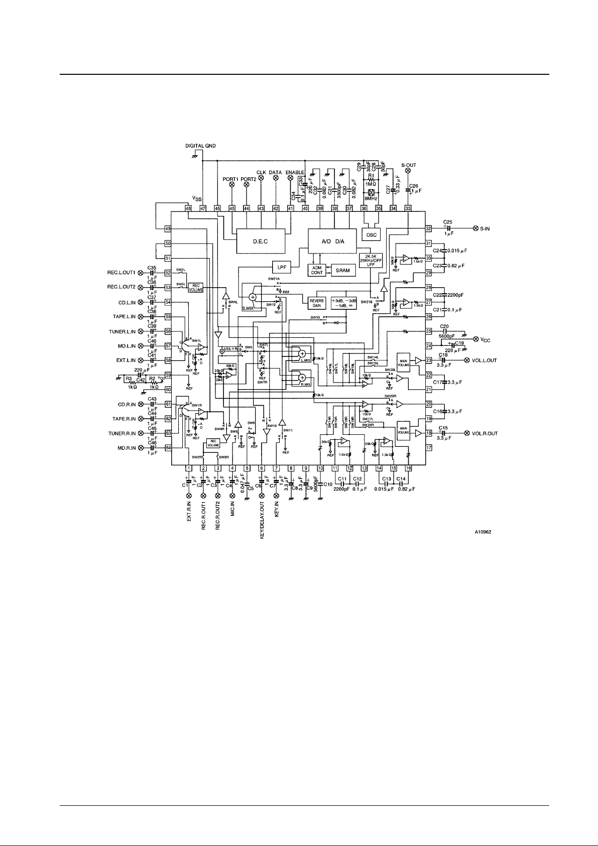
Measurement Circuit
No. 6094-5/22
LV1110NM
Sample Application Circuit

Control Format
A = “Low” level selects the LV1110M.
B1 and B2 specify the data mode (LL, HL, LH, or HH).
D1 to D13 give the data.
A = L, B1 = L, B2 = L
Input function switching
No. 6094-6/22
LV1110NM
D1, D2, D3 Function Notes
L, L, L MUTE SW1 = F
L, L, H CD.IN SW1 = A
L, H, L Tape.IN SW1 = B, VG = 6 dB
L, H, H Tuner.IN SW1 = C, VG = 6 dB
H, L, L MD.IN SW1 = D
H, L, H EXT.IN Sw1 = E, VG = 6 dB
Vocal canceler (When on, set D4, D5, and D6 for L+R mode.)
L H
D7 OFF : SW9 = A ON : SW9 = B
Microphone input
L H
D8 OFF : SW8 = B ON : SW8 = A
Stereo/matrix switching
L H
D10 SW7 = A SW7 = B
S-IN/S-OUT switching
L H
D11 SW OFF SW ON
Delay input switching
Function
L, L SW12 = C
L, H SW12 = A
H, L SW12 = B
Input switching See the Block Diagram for the SW modes.
D4, D5, D6 Function SW5 SW9 SW20
L, L, L L + R B A B
L, L, H L – R B C B
L, H, L L Only A A B
L, H, H R Only C A B
H, L, L Matrix Through B A B
H, L, H Total Through B A A
Key control switching
D9 Function SW7 SW10 SW11
L OFF A/B A B
H ON C B A
No. 6094-7/22
LV1110NM
A = L, B1 = H, B2 = L
Out filter switching
D1, D2 Level
L, L Through
L, H 28 kHz L.P.F.
H, L 5 kHz, L.P.F
H, H 2 kHz L.P.F.
Front ADD effect volume
D12, D13 Level
L, L –∞
L, H –5 dB
H, L –3 dB
H, H +3 dB
Reverberation level
D3, D4, D5 Level
L, L, L –∞
L, L, H –9 dB
L, H, L –7 dB
L, H, H –5 dB
H, L, L –3 dB
H, L, H –2 dB
H, H, L –1 dB
H. H. H 0 dB
Delay
D6, D7, D8 Level
L, L, L 15 ms
L, L, H 20 ms
L, H, L 25 ms
L, H, H 30 ms
H, L, L 40 ms
H, L, H 50 ms
H, H, L 100 ms
H. H. H 120 ms
System muting
L H
D9 Muting on Muting off
L and R muting
L H
D10 Muting on Muting off
Effect R channel ADD
L H
D11 In-phase addition SW13 = A Inverted phase addition SW13 = B
 Loading...