

Page 1
Ordering number : EN5901
LPH-14918-09
Red Laser Diode
LPH-14918-09
LED PRINTHEAD
1. Description
LPH-14918-09 is a printing head for optical printer using one-line LED array of 14464 dots.
It has 128 bit Driver ICs which consist of shift register, latch, strobe and output driver.
It has an effective printing width of 918.4 mm, a resolution of 400 dot/inch and can perform high-speed and high
reliable printing.
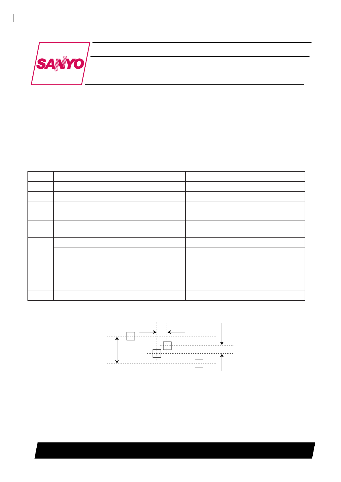
2. Mechanical Characteristics (refer to Fig. LPH14918090-00010-AA) (Ta=25°C)
No. Item Ratings
(1) Array Length 918.5 mm ± 0.5 mm
(2) Number of Emitters 14464 dots
(3) Emitter Size 35µm × 40µm ± 5(with stripe electrode)
(4) Emitter Pitch 63.5µm
(5) Pitch Error (X1) ± 20µm (chip to chip)
± 5µm (inside a chip)
(6) Emitter Y-Direction Error (Y1) Max. 20µm (chip to chip)
Emitter Linearity (Y2 ) Max. 200µm (along LED chips)
(7) lst dot Distance from Origin Point X2=33.3± 0.3mm
Y2=0± 0.2mm
Z=1.2± 0.2mm
(8) Head Dimensions 1015(L) × 38(W) × 38(H)
(9) Head W eight T.B.D.
X1 Y1
Y2
SANYO Electric Co.,Ltd. Semiconductor Bussiness Headquarters
TOKYO OFFICE Tokyo Bldg., 1-10, 1 Chome, Ueno, Taito-ku, TOKYO, 110 JAPAN
31698 GI, (IM
)
No.5901 1/7
Page 2
LPH-14918-09
3. Optical Characteristics (Ta=25°C, SLA-20 TC18.0)
Item Symbol Min. Typ. Max. Unit Remarks
Wavelength λp 665 665 675 nm
Average Light Output IO 0.5 ----µW/dot ❊1
Uniformity1 ID ---- 22.5 % ❊2
Uniformity2 IR ----10 % ❊3
MTF 40 ----%❊4, 1 on / 1 off
❊1 Power meter AQ-2105B (ANDO electric co., Itd.)
❊2 ID = ((Imax-Imin) / (Imax+Imin)) × 100 %
❊3 IR = ((Iave (n) -- Iave (n-1)) / Iave (n-1)) × 100 %
❊4 MTF = ((a-b) / (a+b)) × 100 % (at Drum Surface)
4. Electrical Characteristics
4-1 Electrical Circuit
Item Summary
(1) Equivalent Circuit Refer to LHP14918090-00020-AA
(2) Timing Chart(Pixel Level) Refer to LHP14918090-00030-AA
(3) Data Transfer Method 8 inputs serial transfer (ODD / EVEN)
(4) Clock Frequency Max. 15 MHZ
(5) Interface
(Pin Assignment)
Refer to LPH14918090-00020-AA
4-2 Absolute Maximum Ratings
Item Sym Conditions Min Typ Max Unit Remarks
Supply Voltage VDD T a=25°C-- 0.3 -- 6.5 V
Input Voltage VI Ta=25 °C-- 0.3 --VDD+0.3 V
LED Junctin Temp. Tj ---80°C
Head T emp. Thead ---60°C Al Base
4-3 Recommended operating Conditions (Ta=25°C, Vss=0V)
Item Sym. Conditions Min Typ Max Unit Remarks
Supply Voltage VDD Ta=25°C 4.75 5.0 5.25 V
CLOCK Frequency fC ----15MHZ
Supply Current IP Ta=25°C60A
No.5901 2/7
Page 3
LPH-14918-09
4-4 Electrical Characteristics (Ta=25°C, VDD=5 ± 0.25V)
Item Symbol
"H"Level Input Voltage VIH 0.7VDD --VDD V
"L"Level Input Voltage VIL 0-- 0.3VDD V
"H"Level Input Current I IH
"L"Level Input Current I IL
Supply Current ION
IDD
Conditions
VI=VDD=5.25V
VDD=5.25V
VI=0V
VDD=5V
VI=0V
VDD=5.25V
ALL ON
fc=15MHz
VDD=5.25V
ALL ON
fc=15MHz
Min. Typ. Max. Units Remarks
---- 150 µA
------150 µA
-- 0.9 -- 2.8 -- 5.7 mA STB
--1827 AVDD, VSS
-- 2.8 3.6 A VDD, VSS
5. Environmental Performance
Item Guarantee Range
(1) Operating Temperature 5→45°C
(2) Operating Humidity 10→90 % RH (No Condensation )
(3) Storage Temperature --10→65°C
(4) Storage Humidity 10→90 %RH (No Condensation)
DATA,CLOCK,LOAD,STB
DATA,CLOCK,LOAD,STB
DATA,CLOCK,LOAD
DATA,CLOCK,LOAD
1/4BLOCK ON
6. Life
(1) Operating Conditions
(a) The number of lighting dots is 10 % of all dots on an average.
(b) Electrical Opetation Ratings are typical values. (LED Duty Cycle / line ; 50 % max.)
(2) Judgement Criteria
The point where the average light output declines 30 % from the initial value or
the point where the minimum light output declines 50 % from the initial value.
(3) Life (LED on time)
Min. 1000 hrs.
No.5901 3/7
Page 4

LPH-14918-09
Timing Chart
CLOCK IN
CLOCK OUT
DATA IN
DATA OUT
LOAD IN
LOAD OUT
tsc
tph/tp1
thold
tsl twl
1/fc
tpcr
tpcf
tph
tpl
0.9V
0.1V
tcftcr
0.9V
0.1V
toftor
0.9V
0.1V
tlftlr
DD
DD
DD
DD
DD
DD
STB
tpsr
DO OUT
tpsf
Switching Character
(VDD=4.5 to 5.5V, Tj=0 to 100°C. CL=10pF)
Note Symbol Condition
FREQENCY fc -------15 MHZ
CLOCK Duty Dclk --455055%
DATA IN → CLOCK Setup time tsc --20----ns
DATA Hold time thold --10----ns
CLOCK OUT → DATA OUT Delay T ime
tpcr -tpcf
CLOCK IN → LOAD IN Setup Time ts; --30----ns
LOAD Pulse width tw; --30----ns
STB→ LED ON Delay Time
tpsr ------ 250 ns
tpsf (10kΩ)---- 250 ns
CLOCK IN→ CLOCK OUT tph -----LOAD IN → LOAD OUT Delay Time tpl
CLOCK Rise / Fall Time
tcr -----tcf
LOAD Rise / Fall Time
DATA Rise / Fall Time
tlr -----llf
tor -----tof
Standard
Min Typ Max
10
-46 ns
35 ns
30 ns
30 ns
35 ns
Unit
No.5901 4/7
Page 5

CN3 (18) STB4
CN3 (14) LDAD
CN3 (10) CLOCK3 (0DD)
CN3 (12) CLOCK4 (EVEN)
CN3 ( 6 ) DATA4 (0DD)
CN3 ( 8 ) DATA4 (EVEN)
CN3 (16) STB3
CN3 (14) LDAD
CN3 (10) CLOCK3 (0DD)
CN3 (12) CLOCK4 (EVEN)
CN3 ( 2 ) DATA3 (0DD)
CN3 ( 4 ) DATA3 (EVEN)
(
OPEN
)
(
OPEN
)
(
OPEN
)
(
OPEN
)
(
OPEN
)
(
OPEN
)
(
OPEN
)
(
OPEN
)
(
OPEN
)
(
OPEN
)
(
OPEN
)
(
OPEN
)
(
OPEN
)
CN2 (18) STB2
CN2 (14) LDAD
CN2 (10) CLOCK1 (0DD)
CN2 (12) CLOCK2 (EVEN)
CN2 ( 6 ) DATA2 (0DD)
CN2 ( 8 ) DATA2 (EVEN)
CN2 (16) STB1
CN2 (14) LDAD
CN2 (10) CLOCK1 (0DD)
CN2 (12) CLOCK2 (EVEN)
CN2 ( 2 ) DATA1 (0DD)
CN2 ( 4 ) DATA1 (EVEN)
CN1,4 (1,2,3,4) VDD (POWER)
CN1,4 ( 9 ) VCC (
LOGIC
)
CN1,4 ( 10 )
VSS
(
LOGIC
)
CN1,4 (5,6,7,8) GND (POWER)
DATA1 IN
DATA2 IN
CLOCK1 IN
CLOCK2 IN
LOAD1 IN
Vref
SEL
STB
Rconl
ADJ(--)
ADJ(+)
VSS
VDD
LOAD2 OUT
CLOCK2 OUT
CLOCK1 OUT
DATA2 OUT
DATA1 OUT
OUT 1
OUT 128
Dr -- 1C
input terminal of driverIC
CN2,3 (1,3,5,7,9,11,13,15,17,19,20) VSS (
LOGIC
)
TL317 REG.
0.1µF (104)
1.5µF (155)
15000µF X 4
0.1µF (104)
1.5µF (155)
+ --
IN OUT
ADJ
LED 113
IC 113
LED 85
IC 85
LED 84
IC 84
LED 57
IC 57
LED 56
IC 56
LED 29
IC 29
LED 28
IC 28
LED 1
IC 1
DO1 DO2 DO127 DO128
VDDH
VREF
RCONT
ADJ(+)
ADJ(--)
STB IN
LOAD IN
SEL
DATA1 IN
DATA2 IN
CLOCK1 IN
CLOCK2 IN
LOAD OUT
DATA 1 OUT
DATA 2 OUT
V
DDVDDVSSVSS
CKICK 1 OUT
CKICK 2 OUT
128bit LED Driver
Current
Control
Q1 Q2
Q127 Q128
PO1 PO2
PO127 PO128
D1 D2
D127 D128
64bit X 2 LATCH
64bit X 2 SHIFT REG.
LPH-14918-09
VSS
VSS
VSS
VSS
VSS
VSS
Power CN1/4
6 GND
No. Assign.
7 GND
8 GND
9VCC
10 VSS
SS
11 V
No. Assign. Assign
Logic CN3 CN2
VSS
SS
SS
12 CLK 4 (EVEN) CLK 2 (EVEN)
13 V
14 LOAD LOAD
15 V
VSS
VSS
SS
16 STB 3 STB 1
17 V
VSS
SS
18 STB 4 STB 2
19 V
VSS
SS
20 V
1VDD
2VDD
3VDD
4VDD
No. Assign.
Power CN1/4
5 GND
Pin Assignment (CN1 to 4)
SS
1V
No. Assign. Assign.
Logic CN3 CN2
SS
2 DATA 3 (0DD) DATA 1 (0DD)
3V
4 DATA 3 (EVEN) DATA 1 (EVEN)
SS
SS
5V
6 DATA 4 (0DD) DATA 2 (0DD)
7V
8 DATA 4 (EVEN) DATA 2 (EVEN)
SS
9V
10 CLK 3 (0DD) CLK 1 (0DD)
SS (even IC)
LED Print Head
Block Diagram
No.5901 5/7
1.”SEL” terminal ... open (odd IC) , V
Page 6

Part Name
4
3
2
5
8 15
(38)
27
23
TC
27
ø4
1033.3±0.3
957±1.5(SLA) (WI=950)
502.5
1015±1
985±1
918.4±1
+0.05
0
1
7
8
9
6
10 10
9
99
20
37
38
8
15
10
15
8–M4
8depth
drum surface
original surface
center of connector
B
8depth
ø 4 ×6
+0.05
–0
8depth
1 10
CN4 CN3 CN2 CN1
102.5±1 124.5±1 26.5±1 102.5±1
1 10
19
20
1
2
19
20
1
2
LPH-14918-09
(HIROSE)
HIF3BA-20PA-2.54DSA
1 * heat sink 1 A6063-T5
No. PART CODE BR PART NAME PCS SUMMARY NOTE
2 * cover 1 A6063-T5
3 * S.L.A. 1 SLA-20
4 * S.L.A. holder 1 A6063-T5
5 * side cover 2
6 * substrate 1 FR4
7 * condenser 4 15000µF / 10V *
8 * CN1,4 2 B10P-VH (JST)
9 * CN2,3 2
No.5901 6/7
Page 7

LPH-14918-09
CAUTION
1. No products described or contained herein are intended for use in surgical implants, life-support systems,
aerospace equipment, nuclear power control systems, vehicles, disaster / crime-prevention equipment or
the like, and the failure of which may directly or indirectly cause injury, death or property loss.
2. Anyone purchasing any products described or contained herein for an above-mentioned use shall:
1) Accept full responsibility and indemnify and defend SANYO ELECTRIC CO.,LTD., it’s affiliates,
subsidiaries and distributors or any of their officers and employees, jointly and severally, against any
and all claims and litigation and all damages, costs and expenses associated with such use.
2) Not impose any responsibility for any fault or negligence which may be cited in any such claim or
litigation on SANYO ELECTRIC CO., LTD., it’s affiliates, subsidiaries and distributors or any of
their officers and employees jointly or severally.
3. Information (including circuit diagrams and circuit parameters) disclosed herein is for example only; it is not
guaranteed for mass production, SANYO believes the information disclosed herein is accurate and reliable,
but no guarantees are made or implied regarding it’s use or any infringements of intellectual property rights
or other rights of third parties.
Precautionary instructions in handling gallium arsenic products
Special precautions must be taken in handling this product because it contains, gallium arsenic, which is
designated as a toxic substance by law. Be sure to adhere strictly to all applicable laws and regulations
enacted for this substance, particularly when it comes to disposal.
Manufactured by ; Tottori SANYO Electric Co., Ltd.
Electronics Device Bussiness Headquaters LED Division
5-318, Tachikawa-cho, Tottori City, 680-8634 Japan
TEL: +81-857-21-2137 FAX: +81-857-21-2161
No.5901 7/7
PS
 Loading...