

Page 1
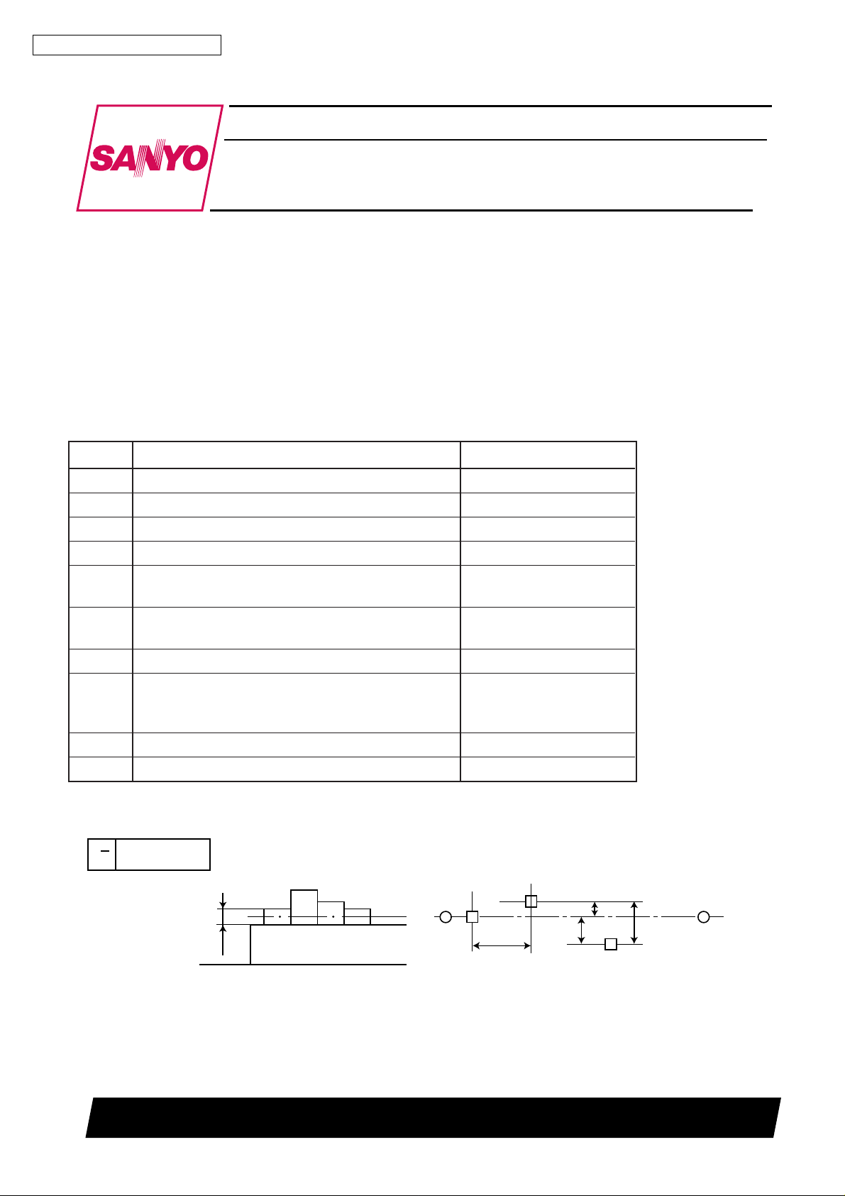
Ordering number : EN5900
LPH-13216-27
Red Laser Diode
LPH-13216-27
LED PRINTHEAD
1. Description
LPH-13216-27 is an LED imaging device which is used to illuminate a moving photoreceptor within an electronic
printer.
It has 2560 bit Driver ICs which consist of shift register, load , strobe and output driver.
It has an effective printing width of 8.31inches, a resolution of 300 dot per inch and can perform high -speed and
high reliable printing.
2. Mechanical Characterristics (refer to Fig. LPH13216270-00010-C1) (Ta=25°C)
No. Item Ratings
(1) Active Length 216.576 ± 0.3mm
(2) Number of Emitters 2560 dots
(3) Emitter Size 48 × 40µm ± 5
(4) Emitter Pitch 84.6µm
(5) Emitter Location Error X1 (chip to chip) ± 20µm
(inside a chip) ± 5µm
(6) Emitter Y Direction Error Y1 (chip to chip) Max. 25µm
Emitter Lincarity YL (along LED chips) 200µm
(7) Emitter Height Lincarity (ZL) Max. 150µm (flatness)
(8) LED Array Distance from origin Holes X2=18.712 ± 0.3mm
(refer to under drawing) Y2=0.0 ± 0.2mm
Z=0.31 ± 0.1mm
(9) Dimensions 262L × 16w × 18H mm
(10) Head Weight approx. 100gr
150µm
Z
(Y2)
Substrate
(Y2)
(X2)
(Y1)
SANYO Electric Co.,Ltd. Semiconductor Bussiness Headquarters
TOKYO OFFICE Tokyo Bldg., 1-10, 1 Chome, Ueno, Taito-ku, TOKYO, 110 JAPAN
31698 GI, (IM
)
No.5900 1/8
Page 2
LPH-13216-27
3. Optical Characteristics (Ta=20°C)
Item Sym. Min Typ Max Unit Remarks
Light W avelenght λp 730 740 750 nm head to head
Light Output (Po MEAN)
Light Output Uniformity ∆Po 0 ±30 %/head Head Overall (2560 LED)
(Intensity)
Light W avelength vs +0.2 nm/°C Peak Wavelength
T emperature
Po MEAN
0.59 0.85 1.1 µW/dot head avcrage (±30%)
4. Electrical Characteristics
4-1 Electrical Circuit
Item Summary
(1) Equivalent Circuit refer to Fig. LPH13216270-00010-C2
(2) Timing Chart refer to Fig. LPH13216270-00010-C3
(3) Switching characteristics refer to Item 5
(4) Data Transfer Methode 1 input serial transfer
(5) Input Data Rate Per Line 10 MHz Max
(6) Inputs Data ; Bits 1-2560
LOAD ; End of Line (Active "H")
Clock ; 10 MHZ Negative edge
STROBE ; LEDs ON Control (Active "L") 4 Line (640×4)
Power ; 5±0.25 V DC 4.4 A Peak 640 LEDs ON
(7) Interface
(Pin Assignment)
refer to Fig. LPH13216270-00010-C1
4-2 Absolute Maximum Ratings (Ta=25 ± 2°C Vss=0V)
Item Sym. Conditions Min Typ Max Unit Remarks
Supply Voltage VDD -- 0.3 6.0 V
Input Voltage VIN -- 0.3 VDD +0.3 V
LED Junction Temperature TJ 80 °C
Head T emperature TH 50 °C
AL base surface of the head
4-3 Recommended operating Conditions (at Vss=0V, Ta=25±2°C)
Item Sym. Conditions Min Typ Max Unit Remarks
Supply Voltage VDD 4.75 5.0 5.25 V
Clock Frequency f(φ)VDD=5V 10 MHZ
Clock Duty tW VDD=5V 45 50 55 %
"H" Level Input Voltage VIH VDD=5V 2.0 VDD V
"L" Level Input Voltage VIL VSS 0.8 V
No.5900 2/8
Page 3
LPH-13216-27
4-4 Electrical Characteristics (Ta=25 ± 2°C,VDD=5V, Vss=0V)
Item Sym.
"H" Level Input Voltage VIH 2.0 VDD V every input
"L" Level Input Voltage VIL 0 0.8 V every input
"H" Level Input Current I IH1VIL=VSS 1.0 µADATA
I IH2VIL=VSS 1.0 µA CLK, LOAD
I IH3VIL=VSS 10 µA STB
"L" Level Input Current I IL1VIL=VSS --1.0 µADATA
I IL2VIL=VSS --80 --250 --500 µA STB
I IL3VIL=VSS ----- ----- --1.0 µA CLK
I IL4VIL=VSS --1.0 µA LOAD
"H" Level Output Current IOH --3.5 --5.0 --6.7 mA/dot
Supply Current IDD
Peak IDD
Average IDD
Conditions
f(φ)=10MHZ
f(φ)=10MHZ
f(φ)=10MHZ
Min Typ Max Unit Remarks
300 mA Out put off
2.4 3.6 4.4 A
A STB duty % Max
AII LEDS ON (640 dots on)
5. Switching Characteristics
Parameter Symbol
CLOCK Frequency f(φ) ----- ----- 10 MHZ
CKOCK Rise / Fall Time tcr ----- ----- 35 ns
tcf ----- ----- 35 ns
LOAD Rise / Fall Time tLr ----- ----- 35 ns
tLf ----- ----- 35 ns
Data Setup Time tSC 30 ----- ----- ns
Data Hold Time thold 10 ----- ----- ns
CLOCK → LOADH Setup T ime tSL 50 ----- ----- ns
LOAD Signal Pulse Width tWL 40 ----- ----- ns
LOAD → STROBE Setup T ime tLS 200 ----- ----- ns
STROBE → DO tpsr ----- ----- 250 ns
Propagation Delay Time tpsf ----- ----- 250 ns
Min Typ Max
Ratings
Unit Remarks
Conditions
(1) VSS = 0V
(2) VDD = 5V
(3) Ta = 25°C ± 2°C
No.5900 3/8
Page 4

LPH-13216-27
6. Enviromental Performance
Item Guarantee Range
(1) Operating Temperature 5 to 40°C
(2) Operating Humidity 10 to 90 % RH (No Condensation and a max wet bulve temperature of 30°C)
(3) Storage Temperature --25 to 70°C
(4) Storage Humidity 10 to 90 % RH (No Condensation)
7. Life
(1) Operating Conditions
LED ON Duty Cycle/Line 10% MAX
(2) Judgement Criteria
The point where the minimum light output declines 10% from the initial value.
(3) Life (LED on time)
100 hours min
No.5900 4/8
Page 5

Timing Chart
CLOCK
LPH-13216-27
1 / f c
0.9V
0.5V
DD
DD
0.1V
DD
DATA
LOAD
t C f
t C r
t s c t h o l d
t S L
t L f
t L r
t W L
t L S
STB
OUT 1-2560
t p s f
t p s r
No.5900 5/8
Page 6

DATA6
CLOCK8
VSS 12
VSS 2
2. 4
VDD
1. 3
LOAD4
STB17
STB25
STB33
STB41
CN - 2
C2C1
OUT
IN
ADJ
#1 #640 #641 #1280
#1281 #1920
#1921 #2560
LED ARRAY1 ( 10)
LED ARRAY11 ( 20)
LED ARRAY21 ( 30)
LED ARRAY31
LED ARRAY40
I C21 ( I C 30)
SI DO 1
CLOCK1
LOAD1
STROBE
VREF
ADJ (3)
ADJ (2)
ADJ (1)
VSS
SEL
VDD
LOAD 2
CLK2
SO DO S4
I C31
SI DO 1
CLOCK1
LOAD1
STROBE
VREF
ADJ (3)
ADJ (2)
ADJ (1)
VSS
SEL
VDD
LOAD 2
CLK2
SO DO S4
I C11 ( I C 20)
SI DO 1
CLOCK1
LOAD1
STROBE
VREF
ADJ (3)
ADJ (2)
ADJ (1)
VSS
SEL
VDD
LOAD 2
CLK2
SO DO S4
I C1 ( I C 10)
SI DO 1
CLOCK1
LOAD1
STROBE
VREF
ADJ (3)
ADJ (2)
ADJ (1)
VSS
SEL
VDD
LOAD 2
CLK2
SO DO S4
SI DO 1
CLOCK1
LOAD1
STROBE
VREF
ADJ (3)
ADJ (2)
ADJ (1)
VSS
SEL
VDD
LOAD 2
CLK2
SO DO S4
I C40
OPEN
8
1
6
R1
R2
TL317 PS
CN -1
D01 D02 D063 D064
VDDH
LOADD2
SOA
SOB
CLOCKA2
64 bit driver
Q1 Q2 Q63 Q64
PO1 PO2 PO063 P064
D1 D2 D63 D64
L 64bit Latch
64 bit Shift Reister
S1
RCONT
ADJ(+)
ADJ(--)
STROBE
SEL
LOAD1
SIA
CLOCKA1
VREF
VDO
VDO
VSSV
SS
Equivalent Circuit
LPH-13216-27
Internal Circuit of D-IC
SS 1
1 STB 4
3 STB 3
5 STB 2
6DATA
7 STB 1
8 CLOCK
Signal Signal
1VDD
2VSS 22V
3VDD
CN-1 CN-2
4VSS 2 4 LOAD
CN-1 : DF11-4DP-2DSA (HIROSE)
CN-2 : DF11-8DP-2DSA (HIROSE)
Pin Assignment
No.5900 6/8
Page 7

Part Name
12.5
1
3.5
16
ø3
18.71±20.3 216.576±0.3 (LED Array)
254±0.1
262±0.5
244
236
4
5
9
1
ORIGINE HOLE
+0.05
0
#1
Data Shift
#2560
5±0.1
3
+0.05
0
3.6 2.0
17.6±0.3
2-C1
C1
8
3.6
MAX 18
ø0.1
5
9.9
9
5.6✕3.6 (substrate)
ø0.1
24.5 70 65 70 24.5
ø3.6±0.1
substrate
Substrate
LED
Drum
2LA20BS
LED
0.31
TC = 15.1 (740nm)
6±0.5
3.5±0.5
3.2±0.1
3.5
ø3.2 + / - 0.1
17
28
4±0.5
17.5
4 - M3
4 - 8
AREA FOR PRODUCT IDENTIFICATION
42
3
152218037
219
1
5.2±0.1
3.5±0.5
CN - 2
HIROSE
DF11 - 8DP -2DSA
CN - 1
HIROSE
DF11 - 4DP -2DSA
LPH-13216-27
SS 1 6 DATA
Pin Assignment
1 STB 4 5 STB 2
3 STB 3 7 STB 1
22V
2 4 LOAD 8 CLOCK
SS
CN-1 CN-2
1VDD
2VSS
3VDD
4V
No.5900 7/8
Page 8

LPH-13216-27
CAUTION
1. No products described or contained herein are intended for use in surgical implants, life-support systems,
aerospace equipment, nuclear power control systems, vehicles, disaster / crime-prevention equipment or
the like, and the failure of which may directly or indirectly cause injury, death or property loss.
2. Anyone purchasing any products described or contained herein for an above-mentioned use shall:
1) Accept full responsibility and indemnify and defend SANYO ELECTRIC CO.,LTD., it’s affiliates,
subsidiaries and distributors or any of their officers and employees, jointly and severally, against any
and all claims and litigation and all damages, costs and expenses associated with such use.
2) Not impose any responsibility for any fault or negligence which may be cited in any such claim or
litigation on SANYO ELECTRIC CO., LTD., it’s affiliates, subsidiaries and distributors or any of
their officers and employees jointly or severally.
3. Information (including circuit diagrams and circuit parameters) disclosed herein is for example only; it is not
guaranteed for mass production, SANYO believes the information disclosed herein is accurate and reliable,
but no guarantees are made or implied regarding it’s use or any infringements of intellectual property rights
or other rights of third parties.
Precautionary instructions in handling gallium arsenic products
Special precautions must be taken in handling this product because it contains, gallium arsenic, which is
designated as a toxic substance by law. Be sure to adhere strictly to all applicable laws and regulations
enacted for this substance, particularly when it comes to disposal.
Manufactured by ; Tottori SANYO Electric Co., Ltd.
Electronics Device Bussiness Headquaters LED Division
5-318, Tachikawa-cho, Tottori City, 680-8634 Japan
TEL: +81-857-21-2137 FAX: +81-857-21-2161
No.5900 8/8
PS
 Loading...