

Page 1
FILE NO
SERVICE MANUAL
L
CD TV
LCD-
PRODUCT CODE No.:
CHASSIS NO. :
P55441-00
P
55441-01
DP55441
113027304
REFERENCE No.:SM0945009-01
Page 2

CONTENTS
1. Safety precautions.................................................................................................
2. Alignment instructions and method of software upgrading.....................................
3. Working principle analysis of the unit...................................................................
4. Block diagram......................................................................................................
5. IC block diagram..................................................................................................
6. Wiring diagram ...................................................................................................
7. Troubleshooting guide..........................................................................................
8. Schematic diagram..............................................................................................
APPENDIX-A: Assembly list
APPENDIX-B: Exploded View
Removing or Installing the Stand
3
5
15
16
18
20
22
27
Page 3

Attention:
please read the following points carefully.
Safety precautions
This service manual is only for service personnel to take reference with. Before
servicing
1. Instructions
Be sure to switch off the power supply before
inserting/plugging in connection wire Anti static measures to be taken (throughout the entire production
process!):
a) Do not touch here and there by hand at will;
b) Be sure to use anti static electric iron;
c) It’s a must for the welder to wear anti static gloves.
Please refer to the detailed list before replacing components that have special safety requirements.
Do not change the specs and type at will.
replacing or welding any components or
2. Points for attention in servicing of LCD
2.1 Screens are different from one model to another and therefore not interchangeable. Be sure to
Use the screen of the original model for replacement.
2.2 The operation voltage of LCD screen is
protecting yourself and the machine when testing the system in the course of normal operation or
right after the power is switched off. Please do not touch the circuit or the metal part of the module
high voltage. Be
sure to take proper measures in
That is in operation mode. Relevant operation is possible only one minute after the power is switched
off.
2.3 Do not use any adapter that is not identical with the TV set. Otherwise it will cause fire or damage
to the set.
2.4 Never operate the set or do any installation work in bad environment such as wet bathroom,
laundry, kitchen, or nearby fire source, heating equipment and devices or exposure to sunlight etc.
Otherwise
2.5 If any foreign substance such as water, liquid, metal slices or other matters happens to fall into the
module, be sure to cut the power off immediately and do not move anything on the module lest it should
cause fire or electric shock due to contact with the high voltage or short circuit.
2.6 Should there be smoke, abnormal smell or sound from the module, please shut the power off at
once. Likewise, if the screen is not working after the power is on or in the course of operation, the
power must be cut off immediately and no more operation is allowed under the same condition.
2.7 Do not pull out or plug in the connection wire when the module is in operation or just after the
power is off because in this case relatively high voltage still remains in the capacitor of the driving
circuit. Please wait at least one minute before the pulling out or plugging in the connection wire.
2.8 When operating or installing LCD please don’t subject the LCD components to bending, twisting or
extrusion, collision lest mishap should result.
2.9 As most of the circuitry in LCD TV set is composed of CMOS integrated circuits, it’s necessary to
pay attention to anti statics. Before servicing LCD TV make sure to take anti static measure and
ensure full grounding for all the parts that have to be grounded.
bad effect will result.
2.10 There are lots of connection wires between parts behind the LCD screen. When servicing or
moving the set please take care not to touch or scratch them. Once they are damaged the screen
be
would
If the connection wires, connections or components fixed by the thermo tropic glue need to disengage
when service, please soak the thermo tropic glue into the alcohol and then pull them out in case of
damage.
unable to work and no way to get it repaired.
3
Page 4

2.11 Special care must be taken in transporting or handling it. Exquisite shock vibration may lead to
breakage of screen glass or damage to driving circuit. Therefore it must be packed in a strong case
before the transportation or handling.
2.12 For the storage make sure to put it in a place where the environment can be controlled so as to
prevent the temperature and humidity from exceeding the limits as specified in the manual. For
prolonged storage, it is necessary to house it in an anti-moisture bag and put them altogether in one
place. The ambient conditions are tabulated as follows:
Temperature
Scope for operation
5
~+ 35
oC
Humidity
2.13 Display of a fixed picture for a long time may result in appearance of picture residue on the
screen, as commonly called “ghost shadow”. The extent of the residual picture varies with the maker
of LCD screen. This phenomenon doesn’t represent failure. This “ghost shadow” may remain
in the picture for a period of time (several minutes). But when operating it please avoid displaying still
picture in high brightness for a long time.
Scope for storage
Scope for operation
Scope for storage
0 ~
+ 40oC
0% ~
90
0% ~ 90%
%
3. Points for attention during installation
3.1 The front panel of LCD screen is of glass. When installing it please make sure to put it in place.
3.2 For service or installation it’s necessary to use specified screw lest it should damage the screen.
3.3 Be sure to take anti dust measures. Any foreign substance that happens to fall down between the
screen and the glass will affect the receiving and viewing effect
3.4 When dismantling or mounting the protective partition plate that is used for anti vibration and
insulation please take care to keep it in intactness so as to avoid hidden trouble.
3.5 Be sure to protect the cabinet from damage or scratch during service, dismantling or mounting.
4
Page 5
2. Alignment instructions
2.1. Test equipment
VG-848 (Video, YPbPr and VGA signal generator)
VG-849 (
Video, YPbPr, VGA and
HDMI signal generator)
FLUKE 54200(TV signal generator)
CA210 (white balancer)
2.2. Power test
Connect main board, power board and IR board according the wiring diagram, connect
the power and press power key(Remote controller or Keypad) button to turn on the TV.
a) Test the pin voltage of P802/power board , the data is shown in table1:
Table1 voltage data of P802
P802 Pin1,2
Voltage
GND 11.6-12.8V
Pin3,4 Pin5,6,7
GND 11.6-12.8V
For55”
Pin8,9 Pin10,11,
4.75-
5.25V
Pin
12
NA
Pin13 Pin14 Pin15 Pin16
On:2V-5.5V
Off: 0-0.5V
<0.6V
2.5-5V
PWM
b) Test the pin voltage of P803/power board, the data is shown in table2:
Table2 voltage data of P803/P804
For55”
P803/P804
Voltage 22.8-25.2V GND NC 2V-5V 2.5-5V PWM NC
Pin1,2,3,4,5 Pin6,7,8,9,10
Pin11 Pin12 Pin13 Pin14
2-5V
5
Page 6
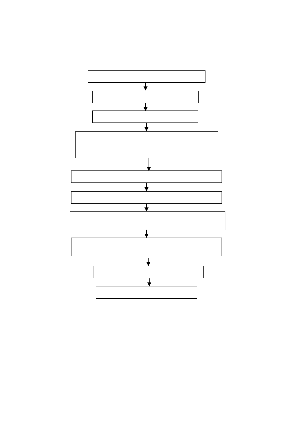
2.3. Alignment flow-chart
The alignment flow-chart is shown as fig-1
Connect to the center signal source and check each
Function of TV (station leaking, analog control, etc.)
Check the output of earphone and speaker.
Check if DDC, HDCP KEY, FLASH are written
Combined test for general assembly
White balance adjustment
Input AV/SVIDEO signal and check the function
Input HD signal and check the function of YPbPr
Input VGA signal and check if the display is normal, check
the function (analog control), horizontal/vertical center, etc.
Input HDMI signal and check if the display is normal, check
the function (analog control), horizontal/vertical center, etc.
Preset ex-factory
Check the accessories and packing
Fig-1 adjustment flow-chart
6
Page 7
2.4. Adjustment instruction
At any input source then press the remote controller buttons “<”, “EXIT” and “>” to enter factory mode.
During Factory menu, if “MENU” or “EXIT” key is pushed, system will exit factory mode.
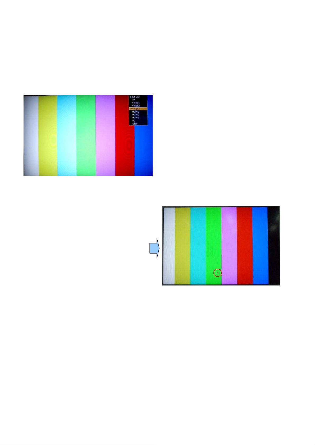
2.4-1. Source Calibration
4-1.1. Set the TV input source to YPbPr; ASTRO-859 signal setting to PG2 program number 933(1080i).
(PG2 mode Timing 933 and Pattern 924 100% Color Bar.)
4-1.2. Entering into factory Mode: Press up or down key of remote control to select “Auto Calibration”, Press
「OK」 key to start.
-> Source calibration performed automatically when finished that will show OK.
7
Page 8

4-1.3. Change input source to PC.
Change Astro-859 Timing to No.953 (640x480@60Hz) and pattern on 953(8step V-grayscale).
Repeat step 4-1.2 to do source calibration,
2.4-2. Color Temperature Adjustment & Check
4-2.1. Set input source.
Set the signal generator Astro-859 timing to PG2-924 on Video & YPbPr, PG2-860 on HDMI, and PG2-963
on PC. Pattern sets 956 on all of the source.
Then press Astro-859 “FORMAT” key and key, then adjust RGB value to R:204, G:204, B:204
8
Page 9
4-2.2. In factory mode OSD menu, select “Color Temperature” item, press “OK” key to enter the item.
R, G, B drive values are set for Warm, Medium, and Cool independently.
4-2.3. Set Color Temperature for “Warm”, “Medium” and “Cool” with following spec table.
Color temperature(for 42")
Color Temp. Cool Medium Warm
x 0.267
y 0.271
Tolerance ± 0.01
0.281
0.288
± 0.01
If the x and y value are larger than specification,
Decrease Red drive from default value.
Increase Blue drive from default value.
If the x or y or both x and y value is/are smaller than specification.
Decrease Blue drive from default value
According to a x and y value, please following adjustment of 1 or 2.
1 If x value is higher than spec
Decrease Red drive from default value.
2 If y value is higher than spec,
Increase Blue drive from default value
4-2.4 Exit Factory Mode:
After finishing adjusting color temperature, press [MENU] or [EXIT] to exit factory mode.
0.301
0.310
± 0.01
9
Page 10

2.5. Items of Factory menu
Vendor may customize design and add adjustment items Factory menu as far as all required items are
included.
Press up and down key can move high light item from Color Temperature Warn -> Color Temperature
Medium -> Color Temperature Cool ->Preset Channel-> Source Calibration -> Reset to Default.
The NVRAM Clear and Reset to Default items will have a check dialog “YES” and “NO” to do or not.
Push “Enter” key can select high light item function. (Press left and right can adjust value)
Display model name, firmware version and released date on top.
10
Page 11

5-1) Color Temperature for Warm
Press up or down key can select high light item function.
Press enter key to enter the item.
Following data for color temp shall be edited manually.
-R, G, B data for each preset.
-Press “Up” or “Down” key to select “R”, “G”, “B” item
-Press “Left” or “Right” key to set the “R”, “G”, “B” value.
-Press “MENU” or “EXIT” item to exit to factory mode
5-2) Color Temperature for Medium
Press up or down key can select high light item function.
Press enter key to enter the item.
Following data for color temp shall be edited manually.
-R, G, B data for each preset.
-Press “Up” or “Down” key to select “R”, “G”, “B” item
-Press “Left” or “Right” key to set the “R”, “G”, “B” value.
-Press “MENU” or “EXIT” item to exit to factory mode
5-3) Color Temperature for Cool
Press up or down key can select high light item function.
Press enter key to enter the item.
Following data for color temp shall be edited manually.
-R, G, B data for each preset.
-Press “Up” or “Down” key to select “R”, “G”, “B” item
-Press “Left” or “Right” key to set the “R”, “G”, “B” value.
-Press “MENU” or “EXIT” item to exit to factory mode
5-4) Time Clear
Press up or down key can select high light item function.
Press “Left” & “Right” key to select the item.
The timer on bottom is to record power on time for panel life.
It was set one time on production only.
5-5) Preset Channel
This is for factory to do some tests.
5-6) NVRAM Clear
Initialize program’s default values to NVRAM for following adjustment items accuracy.
In factory mode it is the first and important step to make sure all values are default value and correct.
- Reset settings: Channel table, Mode table (H/V Position, Clock, Phase), Source dependent setting
(Contrast, Brightness etc.), Common setting (Volume, Language etc.), Parental Control (Rating,
Password etc), Closed Caption.
To avoid a mistake initial process after factory setting is done. This item will have a check dialog to do the
initial or not.
NOTICE:
After this item is processed, the DUT needs to be powered off then AC powered off.
5-7) Full Power
This is for power consumption testing.
To measure the maximum power consumption of TV set, we adjust the value of following items to maximum.
11
Page 12

- Video: Contrast maximum value, Brightness maximum value, Backlight maximum value.
- Audio: Volume maximum value.
Press right key to turn on Full Power and OSD stay display until press enter key to recover from Full Power.
5-8) Source Calibration
Auto Calibration (gain/offset) must be adjusted color by firmware automatic adjustment in PC, and
Video3(Component) input source.
This item will have a result dialog “OK” or “NG”.
5-9) Reset to Default
This function is same as “NVRAM Clear”, but it will power off automatically after processing this function.
5-10) RF Burn In
Use “snow” pattern for burn in. Selected items are “On” and “Off”.
While turn on burn in mode, firmware will automatically turn off “Auto power off” function.
If there is no power supply suddenly, firmware will re-enter burn in mode automatically
when power supply is back.
Pressed the “Power” key, firmware will automatically turn off burn in mode.
- Burn in mode: Source is “TV”, Input Configuration is “Antenna” and channel is NTSC channel 2.
5-11) USB F/W Upgrade
The function is using USB device to upgrade firmware via USB port.
Copy the firmware file to USB device root path.
Execute this function to update firmware, the following OSD will display.
Note: After finishing updated, the system will reboot automatically
5-12) Protocol Switch
This is for debugging only. It is no use for service.
5-13) EDID Write
This is for writing EDID on the VGA source.
12
Page 13
5-14) MEMC Demo Mode
To separate screen into two parts that left side is 60Hz and right side is 120Hz for display.
5-15) MEMC Level
Changing MEMC level to Weak, Medium or Strong.
2.6. Performance check
No
Signal
name
Table4
Signal mode
Resolution
YPbPr
frequency(Hz)
signal format
Vertical
→
Channel Scan, check if there are channels be
Horizontal
frequency
(KHz) (MHz)
Dot clock
frequency
Remarks
6-1 TV function
Connect RF to the center signal source, enter Channel menu
skipped, check if the picture and speaker are normal.
6-2 AV/S-Video terminals
Input AV/S-Video signal, check if the picture and sound are normal.
6-3 YPbPr/YCbCr terminal
Input YPbPr signal (VG-859 signal generator), separately input the YUV signals listed in table4 and check if
the display and sound are normal at any situation (power on, channel switch and format convert, etc.)
1
2
3 720P/60
4 1080i/60 1920x1080 60 33.75 74.25
5 1080p/60 1920x1080 60 67.5 148.5
480i 720x480 59.94 15.73 27
480P 720x480 59.94 31.47 27
1280x720 60 45 74.25
6-4
PC(
VGA) terminal
Input
PC(V
GA) signal (VG-859 signal generator), separately input the signals listed in table5 and check the
display and sound. If the image is deflection of the Horizontal and Vertical, select Menu->PC->Auto Adjust to
perform auto-correct.
Signal mode
No
Signal
name
1
VGA 640 x 480
2 SVGA 800 x 600
3
XGA 1024 x 768
Resolution
Table5
PC
signal format
Horizontal
frequency
Vertical
frequency(Hz)
59.941 31.469 25.175
60.317 37.879 40
60.004 48.363 65
(KHz) (MHz)
Dot clock
frequency
Remarks
4
W-XGA
5
6 SXGA 1280 x 1024
1280 x 768
1360 x 768
59.87 47.776 79.5
60.015 47.712 85.5
60.02 63.981 108
13
Page 14
6-5 HDMI terminal
Input HDMI signal (VG-859 signal generator), separately input the signals listed in table6 and check the display
and sound (32KHz, 44.1KHz, 48KHz) at any situation (power on, channel switch and format convert, etc.)
Table6
HDMI
signal format
No
1
2
3
Signal mode
Signal
name
VGA 640 x 480 59.94 31.469 25.175
SVGA 800 x 600 60.317 37.879 40
XGA 1024 x 768 60.004 48.363 65
Resolution Vertical frequency(Hz) (KHz) (MHz)
Horizontal
frequency
Dot clock
frequency
Remarks
4
W-XGA
5
6
SXGA 1280 x 1024
7
8
9 720P/60
10 1080i/60 1920x1080 60 33.75 74.25
11 1080p/60 1920x1080 60 67.5 148.5
12 1080p/24 1920x1080 24 27 74.25
480i 720x480 59.94 15.734 27
480P 720x480 59.94 31.5 27.03
1280 x 768 59.87 47.776 79.5
1360 x 768 60.015 47.712 85.5
60.02 63.981 108
1280x720 60 45 74.25
6-6 other functions check
a) Check the turn on/turn off timer, sleep timer, picture/sound mode, OSD, stereo and analog TV Close Caption, V-
Chip, etc.
14
Page 15

3. Working principle analysis of the unit
1. NTSC/ATSC signal flow:
Antenna reception NTSC/ATSC signal will be send to tuner U32,
demodulating and output
These
differential IF+ IF- signal
interlace and scaler, then output LVDS level drive for panel display.
The
differential signals
amplifying, bass adjusting and volume control, the sound signal will
I2S signal by
scaler
2. AV VIDEO signal flow
Video path AV signal switch
differential IF+ IF- signal .
will send to the master control IC U1 to video/MPEGII decode, de-
will be fed into U1 to demodulate audio signals , after demodulating, pre-
IC
and sent to digital amplifier U5 amplifying,
by menu “Inpput list”
then Tuner will be
be transform into digital
then output to speaker.
via terminal socket, the signal and the Video1
path AV signal will be fed to U1 to perform video decode, de-interlace and scaler, then output LVDS
drive level for panel display.
Audio signal from AV
the sound signal will be
amplifying,
output to speaker.
3. PC/YPrPb signal flow
terminal
via matched resistance is fed to U1 to bass adjust and volume control,
transfered into digital I2S signal by scaler IC
and sent to digital amplifier U5
PC and the Video2 and Video3 path YPbPr signal are via terminal sent to U1 A/D conversion,
output R/G/B of 24 bit to back end module to digital decode, image scale, then send to LVDS
level drive for panel display.
Sound signal of PC/YPrPb
terminal
via matched resistance
and
sent to U1 to bass adjust and
volume control, the sound signal will be transform into digital I2S signal by scaler IC and sent to digital
amplifier U5 amplifying,
4. HDMI signal flow
HDMI video signal via terminal sent to
level for panel display. HDMI audio signal via decoder built-in terminal sent to
to bass adjust and volume control, the sound signal will
scaler IC and sent to digital amplifier
then output to speaker.
U1
U5
amplifying,
to digital decode, image scale, then output LVDS drive
U1 is
be
transform into digital I2S signal by
fed to back end
then output to speaker.
5. MEDIA signal flow
The JPEG file via USB terminal send to U1 to MPEG decode , image scale , then output LVDS
drive level for panel display .
15
Page 16
4. Block diagram-SANYO 55” ATSC model System Diagram
DDRII 512M
ProMOS
V59C1512164QDJ25
16
Page 17

Block diagram-POWER-55”
17
Page 18

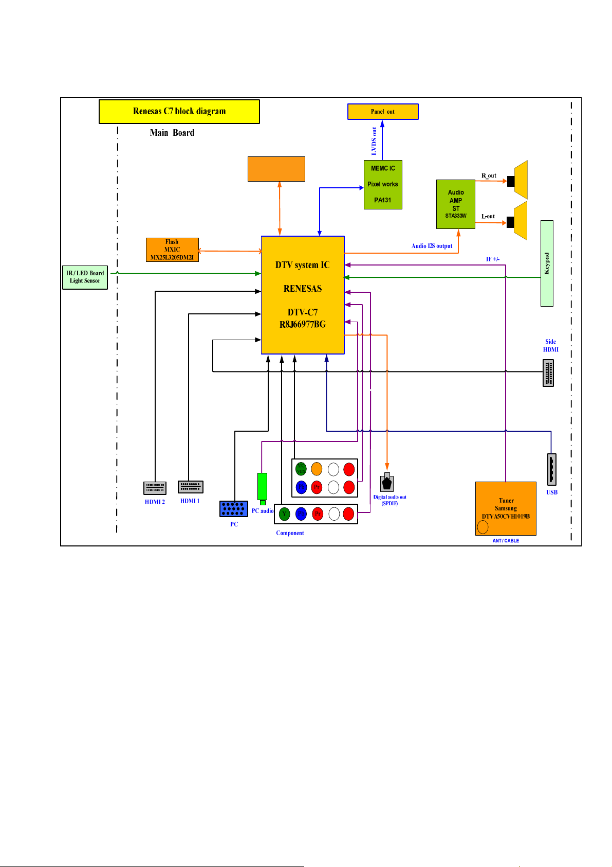
5.IC block diagram
5-1. Renesas , R8J66977BG-RFJZ
Model - SubModel Surround Maximum panel size Number of HDMI ports
R8J66977BG-RFJZ Simple surround FullHD
(1920 x 1080)
Features
Main CPU
32bit RISC Super-H architecture SH3 CPU core
emodulator
D
ATSC A/53 compliant 8VSB receiver /w QAM.
IF AGC control interface x1ch
System decoder (Stream demultiplexer)
Video and audio ES stream filtering x1
Section filtering: max. 32 PIDs
MPEG video decoder
Single ISO-13818-2 MP@ML or MP@HL support
Supports decoding of all ATSC-compliant formats
JPEG decoder
Decode Base-line JPEG file
2D Graphics
CEA-608/CEA-708-B closed caption support
Display processor, Video input/output
Full 10bit processing
MPEG Noise Filter (De-blocking/De-ringing)
Over Drive (Panel resolution : up to WXGA)
Inputs : CVBS x3, Y/C x2, YPbPr x2, RGB x1, HDMI x3
Outputs : 10-bit dual LVDS
udio decoder, Audio input/output
A
ATSC A/52 Clear QAM compliant audio decoding support
Sound Demodulator
Inputs : SIF x1, Stereo x6
Outputs : PCM (I2S) x2, S/PDIF x1, Stereo x1
Peripheral interfaces
UART x1, Legacy serial interface x2, USB High Speed x1
General purpose I/Os
Memory interfaces
Serial Flash
16b width DDR2 800Mbps(5-5-5) SDRAM x 1
Power, clock and package
1.26(±0.06)V, 1.82(±0.08)V, 3.3(±0.15)V
25MHz X’tal
376pin PBGA
3
18
Page 19

5-2. C7 Block diagram
19
Page 20

5.3 Pixelworks PA131
Features
•
• Fourth Generation MotionEngine Technology
••
– Significantly improved Content Adaptive Motion Estimation and Motion
Compensation (MEMC) using Pixelworks’ proprietary technology
– Support for up to 120Hz displays at 1080p and WUXGA resolutions
– Progressive hardware film mode detection with 3:2/2:2 inverse pull down and
programmable random cadence detection
– 10-bit Full HD Video processing in 4:2:2 format
– 10-bit graphics in 4:4:4 format
– ntegrated Overdrive
– Programmable OSD region protection (up to 5 OSD regi
– Automatic OSD/logo detection and protection
– Support for demo modes
•
•Input Port
••
– 24/30-bit LVDS receiver
– 170MHz maximum input clock frequency for 1080p@60Hz and WUXGA@60Hz
– Spread-spectrum supported
– Control Interfaces: Two-wire serial interface, GPIO, UART and SPI
•
•Integrated MCU
••
– Master mode: no external CPU is needed. PA131 operates as the main controller
chip
– Slave mode: PA131 controlled by an external CPU
– Watch-dog
– Multiple timers
– SPI flash
– Interrupt controller
– UART
ons)
– JTAG
•Memory Controller
•
•
•
– 16-bit DDR2 up to 333MHz clock rate
– 256Mb/512Mb/1Gb
– Spread-spectrum supported
•
•Output Port
••
– 4 channel LVDS transmitter up to 595MHz
– Supports dual-frame output
– Support for Spread-spectrum
20
Page 21

5-4. PA131 Block diagram
21
Page 22
55” Block
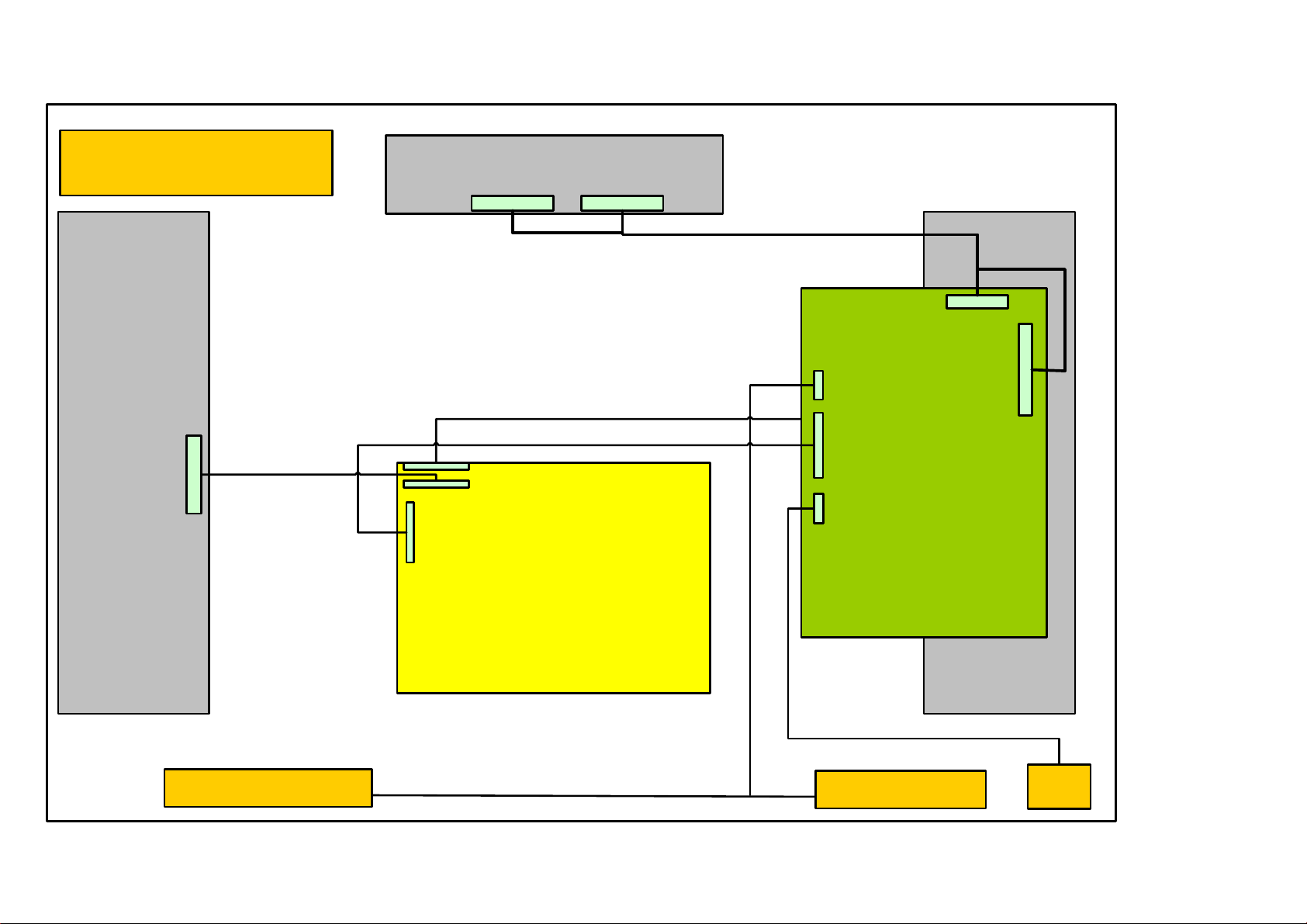
55" Connection
Inverter
Board
Power-16 pin
T-Con. Board
To inverter
Inverter-14 pin
Inverter-14 pin
Power Board
CN2
Speaker-4 pin
CN1
Power-16 pin
Main Board
CN5
IR / 6 pin
CN16
LVDS -30 pin
CN15
LVDS -40 pin
Inverter
Board
Speaker
20
Speaker
Inverter
oard
B
IR Board
Page 23

3.3V
1-3V
5V
0-4V
3.1V
3.5V
6.Wiring Connection
VTV-L55712 VTV-L55712 V
CN1 CN3 CN15 CN16
1 GND 1 5V 1 VDD 21 GND 1 TX3OUT0M 16 TX3OUT4P
2 GND 2 IR Receive 2 VDD 22 GND 2 TX3OUT0P 17 GND
3 12V 3 GND 3 VDD 23 Panel SEL 3 TX3OUT1M 18 GND
4 12V 4 RED LED 4 VDD 24 GND 4 TX3OUT1P 19 TX4OUT0M
5 GND 5 GREEN LED 5 TX1OUT0M 25 TX2OUT0M 5 TX3OUT2M 20 TX4OUT0P
6 GND 6 Light Sensor 6 TX1OUT0P 26 TX2OUT0P 6 TX3OUT2P 21 TX4OUT1M
TV-L55712 VTV-L55712
7 GND
7 TX1OUT1M 27 TX2OUT1M 7 GND 22 TX4OUT1P
8 12V CN2 8 TX1OUT1P 28 TX2OUT1P 8 GND 23 TX4OUT2M
9 12V 1 SPK_OUTR+ 9 TX1OUT2M 29 TX2OUT2M 9 TX3CLKM 24 TX4OUT2P
10 5V 2 SPK_OUTR- 10 TX1OUT2P 30 TX2OUT2P 10 TX3CLKP 25 TX4CLKM
11 5V 3 SPK_OUTL- 11 GND 31 TX2CLKM 11 GND 26 TX4CLKP
12 5V 4 SPK_OUTL+ 12 GND 32 TX2CLKP 12 GND 27 TX4OUT3M
13 Power ON
14 AC OFF Detect
15 BACKLIGHT_ADJ
16 BACKLIGHT_EN
13 TX1CLKM 33 TX2OUT3M 13 TX3OUT3M 28 TX4OUT3P
14 TX1CLKP 34 TX2OUT3P 14 TX3OUT3P 29 TX4OUT4M
15 GND 35 TX2OUT4M 15 TX3OUT4M 30 TX4OUT4P
16 GND 36 TX2OUT4P
17 TX1OUT3M 37 GND
18 TX1OUT3P 38 DCR_EN
19 TX1OUT4M 39 BACKLIGHT_ADJ
20 TX1OUT4P 40 DCR_ADJ
21
Page 24

1
1
2
2
3
3
4
4
5
5
6
6
7
7
8
8
9
9
10
10
11
11
12
12
13
13
14
14
5V
1-3V
1-3V
5V
0V
Power/B
P802
1 GND
2 GND
3 12V
4 12V
5 GND
6 GND
7 GND
8 12V
9 12V
10 5V
11 5V
12 DIM_S
13 Power ON
14 ACD
15 BL_ADJ
24V
24V
24V
24V
24V
GND
GND
GND
GND
GND
NC
BLON
DIM
DIM_S
P803
P804
24V
24V
24V
24V
24V
GND
GND
GND
GND
GND
NC
BLON
DIM
DIM_S
16 BL_EN
22
Page 25

7. Trouble Shooting
7-1. Fault clearance
22
Page 26

pin #1
7-2. Troubleshooting guide
The flow chart shown below will help you to troubleshoot your Televison set with it doesn’t display
normally. Each procedure offers a simple way to check for system errors. Before starting, ensure
that there is a signal in and that the Televison is turned on.
7.2-1 Power LED no light
Change to new power board.
P/N : PK101V2540I (SSC55T)
23
Page 27

7.2-2 Has audio but no video out
P802,
pin#16
Change to new power board.
P/N : PK101V2540I
(SSC55T)
24
Page 28

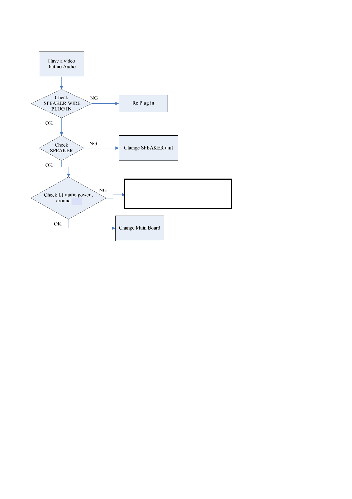
7.2-3 Has video but no audio out
Have a video but no
sound
Check volume or
Mute
OK
Check Input
source
OK
Check speaker Change speaker
OK
MUTE
NG
NG
Cancel mute function
Or adjust volume up
Change source device
Change main pcb
25
Page 29
Change to new power board.
P/N : PK101V2540I (SSC55T)
12V
26
Page 30

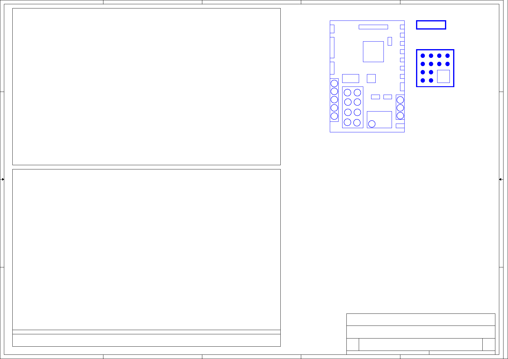
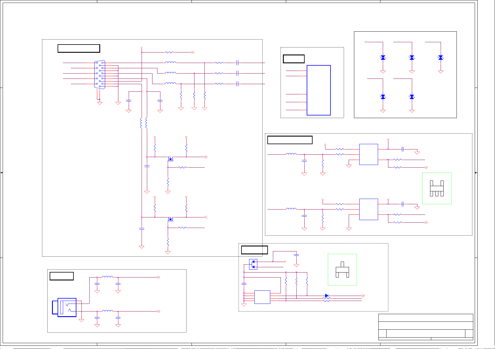
8.SCHEMATIC DIAGRAM
ELECTRON-55"
Page 31
5
4
3
2
1
Sheet Index
FW1
Page 03 - System Power
Page 04 - C7 & MCU / Key
MAIN PCB1
MAIN PCB1
FW1
FIRMWARE
FIRMWARE
FW SSC55T REV1.0
FW SSC55T REV1.0
Page 05 - C7 & Tuner Input
Page 06 - C7 & Video Input
D D
Page 07 - C7 & VGA Input
EMIcover1
EMIcover1
Page 08 - C7 & HDMI Input
Page 09- C7 & Audio Input
Page 10 - C7 & Debug IO / FLASH ROM
Page 11- C7 & Power
EMIcover-C7
EMIcover-C7
Page 12 - C7 & DDRII-800
Page 13 - C7 & LVDS Output
Page 14 - C7 & Audio Out
Page 15 - Audio Amplifier
Page 16 - PA131_LVDS
Page 17 - PA131_DDR2
C C
Page 18 - PA131_MISC
VTV-L55712 REV:1
VTV-L55712 REV:1
Page 19 - PA131_POWER
Page 20 - Board_Power_Supply
Notice
1. All Res. is 0603.
2. All Cap. is 0402 (<=0.47uF), 0603 (<=1uF), 0805 (<=10uF).
0402
NPO 5pF/50V, 10pF/50V, 22pF/50V, 27pF/50V, 33pF/50V, 36pF/50V, 47pF/50V, 220pF/50V
X7R 100pF/25V, 470pF/25V, 1000pF/25V, 2200pF/25V, 3300pF/25V, 0.01uF/25V, 0.01uF/50V, 0.022uF/25V
B B
X5R 1uF/10V
Y5V 0.1uF/25V, 0.33uF/10V, 0.47uF/10V
0603
Y5V 0.1uF/50V, 0.47uF/25V, 1uF/16V
X5R 10uF/6.3V
0805
X5R 4.7uF/16V
Y5V 0.47uF/50V, 0.68uF/50V, 1uF/50V, 3.3uF/10V, 10uF/10V
1206
Y5V 4.7uF/35V
1210
A A
Y5V 10uF/35V
3. The mark "#" to indicate that Part disuse.
Renesas Scaler
5
COMPAL OPTOELECTRONICS CO., LTD
COMPAL OPTOELECTRONICS CO., LTD
COMPAL OPTOELECTRONICS CO., LTD
Title
Title
Title
SCHEMATIC,M/ B VTV-L55712,S SC55T
SCHEMATIC,M/ B VTV-L55712,S SC55T
SCHEMATIC,M/ B VTV-L55712,S SC55T
Size Document Number Rev
Size Document Number Rev
Size Document Number Rev
Custom
Custom
Custom
Date: Sheet
Wednes day, February 09, 2011
Date: Sheet
Wednes day, February 09, 2011
Date: Sheet
4
3
Wednes day, February 09, 2011
2
401C41
401C41
401C41
of
of
of
2 20
2 20
2 20
1
1A
1A
1A
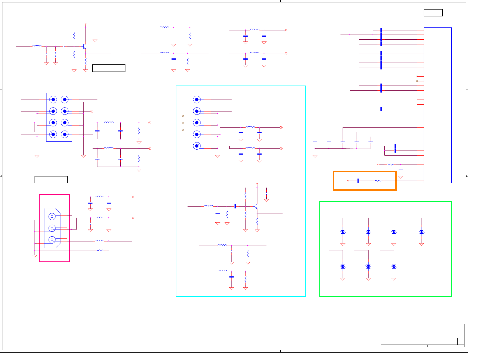
Page 32

5
Power Module Input
CN1
CN1
JWT A2001WV2-16P
JWT A2001WV2-16P
1
2
3
4
5
6
7
8
D D
C C
9
10
11
12
13
14
15
16
GND
Audio PW
L1 B201212K800TM
L1 B201212K800TM
L0805D
L0805D
1 2
L2 B201212K800TM/NC
L2 B201212K800TM/NC
L0805D
L0805D
1 2
R435
R435
10K/NC
10K/NC
2010/12/28 LG panel DIM select
POWER_ON2
PG
BKLT_EN
R434
R434
10K/NC
10K/NC
GND
P_DA MP
P_DAMP
P12V
P5V
POWER_ON2 P4
C425
C425
10uF/10V/0805
10uF/10V/0805
2N7002E_ON
2N7002E_ON
Standby Power
FB10
FB10
KHB0603N121SA
KHB0603N121SA
10uF/10V/0805
10uF/10V/0805
C329
C329
R221 10K/1%/NCR221 10K/1%/NC
GND
P5V
B B
R308
R308
10K/1%
10K/1%
C318
C318
0.1uF/10V/0402
0.1uF/10V/0402
U43
U43
GND
G9141T11U
G9141T11U
3
5
/SHDN
OUT
1
4
IN
SET
GND
2
GND GND
R242
R242
23.2K/1%
23.2K/1%
R307
R307
10K/1%
10K/1%
POWER_ON1P4
LCD PANEL POWER MosFET
12
R17
R17
0/1206
0/1206
R1206D
R1206D
+
+
C58
C58
0.1uF/50V
0.1uF/50V
SE100uF/16V
SE100uF/16V
A A
PANEL _VENP4
5
GND
PANEL _VEN
12
GND
R25 22KR25 22K
1 2
R26
R26
5.6K
5.6K
P5VP12V
12
R18
R18
0/1206/NC
0/1206/NC
U7
R1206D
R1206D
APM4461U7APM4461
1
S1
2
S2
3
12
12
12
R19
R19
C65
C65
3.3K
3.3K
1 2
GND
12
C66
C66
10uF/16V/0805
10uF/16V/0805
C0805D
C0805D
GND
S3
C75
C75
G4D1
1uF/16V/NC
1uF/16V/NC
C0603D
C0603D
R39
R39
24K
24K
12
R280R28
0
GND
1 2
CE
B
Q2
MMBT3904LQ2MMBT3904L
GND
4
R7 0R7 0
12
R10
R10
100K/0402
100K/0402
GND
12
C49
C49
10uF/10V/0805/NC
10uF/10V/0805/NC
C0805D
C0805D
P5V
GND
R367
R367
P5V
560
560
R368
R368
D
1K/1%/0402
1K/1%/0402
G
CE
S
GNDGND
Q44
Q44
MMBT3904L
MMBT3904L
GND
3.3V_STB
C330
C330
C197
C197
10uF/10V/0805
10uF/10V/0805
0.1uF/10V/0402
0.1uF/10V/0402
R20 30K/1%/0402R20 30K/1%/0402
1 2
POWER_ON1
8
D4
7
D3
6
D2
5
12
R22
R22
1K/1206
1K/1206
R1206D
R1206D
GND
C70
C70
1uF/16V/NC
1uF/16V/NC
C0603D
C0603D
Vds = -24V
Vgs = -2.5V/-4.5V/-10V
Id = -2A/-4A/-7A
(APM4461)
4
B
Q45
Q45
R369 100/1%/0402R369 100/1%/0402
3.3V_STB
P5V
R4
2.2KR42.2K
47K
47K
B
47K
47K
R8 0R8 0
1 2
12
C72
C72
0.1uF/50V/NC
0.1uF/50V/NC
GND
GND
R297 10K/0402R297 10K/0402
1 2
12
C69
C69
1uF/16V
1uF/16V
C0603D
C0603D
GND GND
L14 B201212K800TM
L14 B201212K800TM
1 2
R13
R13
22K
22K
ACOFF_ DET
Q38
Q38
PDTC114ET
PDTC114ET
E C
GND
1K/1%/0402/NC
1K/1%/0402/NC
R36 1K/1%/0402/NCR36 1K/1%/0402/NC
R370
R370
10K/0402/NC
10K/0402/NC
Q48
Q48
APM2301AAC
APM2301AAC
G
CE
B
Q3
MMBT3904LQ3MMBT3904L
L0805D
L0805D
COLLECTOR
DTC124EK
SOT-23B
BASE
R35
R35
12
Q46
Q46
MMBT3904L/NC
MMBT3904L/NC
BACKLIGH T_EN P4
L17
L17
B201212K800TM
B201212K800TM
L0805D
L0805D
1 2
DS
VDD_L CD
12
C57
C57
0.1uF/50V
0.1uF/50V
GND
EMITTER
ACOFF_ DET P4
3.3VD
3.3V_STB
R330
R330
10K/1%/NC
10K/1%/NC
1 2
R32
R32
CE
1K/1%/NC
1K/1%/NC
1 2
B
GND
12
C71
C71
10uF/10V/0805
10uF/10V/0805
C0805D
C0805D
GND GND GND
VDD_L CD
12
GND
R11 0R11 0
1 2
R12 0/NCR12 0/NC
1 2
C67
C67
100pF/25V/0402/NC
100pF/25V/0402/NC
12
C78
C78
10nF/25V/0402
10nF/25V/0402
BACKL IGHT_ADJ P4,13
DCR_ADJ P13
3.3VD
12
C86
C86
0.1uF/10V/0402
0.1uF/10V/0402
3
DC - DC FROM VCC TO 1.25V(2A)
P5V
KHB0805W121SA_6A
KHB0805W121SA_6A
FB68
5V -> 1.8V
P5V
3
+
+
SE100uF/16V
SE100uF/16V
5V -> 3.3V
POWER_ON1P4
C196
C196
FB68
10uF/10V/0805
10uF/10V/0805
3.3VA
3.3VD
12
C50
C50
0.1uF/10V/0402
0.1uF/10V/0402
GND
C372
C372
POWER_ON1
GND GND
C379
C379
0.1uF/10V/0402
0.1uF/10V/0402
0.1uF/10V/0402
0.1uF/10V/0402
R45 10K/1%/0402/NCR45 10K/1%/0402/NC
1 2
1 2
R24 10K/1%/0402R24 10K/1%/0402
R40
R40
20K/1%/0402/NC
20K/1%/0402/NC
P5V
R15 10K/0402R15 10K/0402
1 2
C41
C41
1uF/16V
1uF/16V
C0603D
C0603D
12
C74
C74
1uF/16V
1uF/16V
C0603D
C0603D
GND
R93 9.09K/1%/0402R93 9.09K/1%/0402
1 2
1.25VD
1 2
GND
1.25VD
R18210R182
10
C378
C378
GND
12
C43
C43
0.1uF/10V/0402
0.1uF/10V/0402
1 2
GND
GND
APM2301AAC
APM2301AAC
R296 10K/0402R296 10K/0402
1 2
B
12
GND GND
12
R96
R96
10K/NC
10K/NC
R95
R95
9.09K/1%/0402
9.09K/1%/0402
12
12
C73
C73
C0603D
C0603D
1uF/16V
1uF/16V
GND
R94 9.09K/1%/0402R94 9.09K/1%/0402
1 2
R97
R97
9.09K/1%/0402
9.09K/1%/0402
1 2
GND
10uF/16V/0805
10uF/16V/0805
GND
U2
G5694U2G5694
8
VIN
LX
1
VCC
FB
5
EN
REF
PGND
GND
THEM_PAD
6
3
9
GND GND
5VSW
Q47
Q47
DS
C32
C32
C34
C34
+
+
G
SE100uF/16V
SE100uF/16V
CE
GND
Q1
MMBT3904LQ1MMBT3904L
U6
AX6615U6AX6615
4
VO
VIN
3
VO
VPP
2
ADJ
POK
1
GND
VEN
ThPad
9
GND
U8
AX6615U8AX6615
5
VIN
6
VPP
7
POK
8
VEN
ThPad
9
12
GND
C317
C317
1uF/16V
1uF/16V
C0603D
C0603D
GND
12
R98
R98
10K/NC
10K/NC
C192
C192
1uF/16V
1uF/16V
C0603D
C0603D
5
6
7
8
Independent TUNER voltage
P12V
C434
C434
C413
C413
0.1uF/50V
0.1uF/50V
GND
FOR TUNER
2
L28 2.2uH/3.8AL28 2.2uH/3.8A
7
C347 47pF/50V/0402C347 47pF/50V/0402
4
R355 9.09K/1%R355 9.09K/1%
2
R354 16K/1%R354 16K/1%
C191
C191
0.1uF/10V/0402
0.1uF/10V/0402
GND GND
Vout=0.8Vx (1+R1/R2)
U3 G1117-3.3V- 252U3 G1117-3.3V- 252
3
Vin
12
0.1uF/10V/0402
0.1uF/10V/0402
GND
R100
R100
12.7K/1%
12.7K/1%
1 2
R101
R101
10K/1%
10K/1%
1 2
GND
4
VO
3
VO
2
R106
1
ADJ / GND
10uF/10V/0805
10uF/10V/0805
R106
12.7K/1%
12.7K/1%
1 2
R103
R103
10K/1%
10K/1%
1 2
GND
2
C436
C436
1
2
ADJ
GND
U31
U31
SSD9117-5.0V-252
SSD9117-5.0V-252
VIN3VOUT
1.25VD
C356
C356
PVM330uF/6V
PVM330uF/6V
2
Vout
C35
C35
+
+
ADJ/GND
SE100uF/16V
SE100uF/16V
1
GND
GND
1.8A
12
C51
C51
C52
C52
+
+
PVM330uF/6V
PVM330uF/6V
10nF/25V/0402
GND GND GND
10nF/25V/0402
1.8D
C60
C60
+
+
SE100uF/16V
SE100uF/16V
GND GND G ND
5V_ TUNER
C415
C415
0.1uF/10V/0402
0.1uF/10V/0402
12
10nF/25V/0402
10nF/25V/0402
12
GND
B201212K800TM/NC
B201212K800TM/NC
C59
C59
C36
C36
10nF/25V/0402
10nF/25V/0402
12
C53
C53
0.1uF/10V/0402
0.1uF/10V/0402
L0805D
L0805D
12
12
C37
C37
0.1uF/10V/0402
0.1uF/10V/0402
GND
L68
L68
1 2
C61
C61
0.1uF/10V/0402
0.1uF/10V/0402
1
L7 B201212K800TM
L7 B201212K800TM
L0805D
L0805D
1 2
12
12
L69
L69
B201212K800TM/NC
B201212K800TM/NC
L0805D
L0805D
L13 B201212K800TM
L13 B201212K800TM
L0805D
L0805D
1 2
L67 B201212K800TM
L67 B201212K800TM
L0805D
L0805D
1 2
L15 B201212K800TM
L15 B201212K800TM
L0805D
L0805D
1 2
12
Title
Title
Title
Size Document Num ber Rev
Size Document Num ber Rev
Size Document Num ber Rev
Custom
Custom
Custom
Date: Sheet
Date: Sheet
Date: Sheet
3.3VA
12
C39
C39
C38
C38
10nF/25V/0402
10nF/25V/0402
10uF/10V/0805
10uF/10V/0805
C0805D
C0805D
GND GNDGND
12
C54
C54
10uF/10V/0805
10uF/10V/0805
C0805D
C0805D
GND GND GNDGND
12
C376
C376
12
C186
C186
10nF/25V/0402
10nF/25V/0402
10uF/10V/0805
10uF/10V/0805
C0805D
C0805D
1.8VD
12
C63
C63
C62
C62
10nF/25V/0402
10nF/25V/0402
10uF/10V/0805
10uF/10V/0805
C0805D
C0805D
COMPAL OPTOELECTRONICS CO., LTD
COMPAL OPTOELECTRONICS CO., LTD
COMPAL OPTOELECTRONICS CO., LTD
SCHEMATIC, M / B VTV-L55712, SSC55T
SCHEMATIC, M / B VTV-L55712, SSC55T
SCHEMATIC, M / B VTV-L55712, SSC55T
401C41
401C41
401C41
Wednesday, February 09, 2011
Wednesday, February 09, 2011
Wednesday, February 09, 2011
1
12
C55
C55
10nF/25V/0402
10nF/25V/0402
1.8VIF
1.8VA
12
GNDGNDGND
12
GNDGNDGND
C40
C40
0.1uF/10V/0402
0.1uF/10V/0402
12
C346
C346
0.1uF/10V/0402
0.1uF/10V/0402
C64
C64
0.1uF/10V/0402
0.1uF/10V/0402
3.3VA
12
C56
C56
0.1uF/10V/0402
0.1uF/10V/0402
1.8VA
1.8VIF
1.8VD
3 20
3 20
3 20
of
of
of
1A
1A
1A
Page 33

5
3.3V_STB
3.3V_STB
C7 MCU
2010/1/3 MEMC UART to VGA romve
D D
MEMC Reset
MEMC F/W Flash
POWER_ON3P20
RSTnP18
TP31TP31
PANEL_SELP13
SPICS0P18
DAMP_RESETNP15
2010/12/15 R37 0 change to 10K
Check
PC_HSYNCP7
C C
B B
PC_VSYNCP7
ACOFF_D ETP3
POWER_ON2P3
CUT_LEAKP11
POWER_ON1P3
HDMI_CEC_C7P8
HDMI_HPD0P8
HDMI_HPD1P8
HDMI_HPD2P8
3.3V_STB
R760
R760
10K/0402
10K/0402
R0402D
R0402D
PANEL_SEL
DAMP_RESETN
1 2
R37 10K/0402
R37 10K/0402
R0402D
R0402D
R31
R31
10K/0402
10K/0402
R0402D
R0402D
1 2
12
MODIFY 2010.11.06
1 2
4
R30
R30
56K/0402
56K/0402
R0402D
R0402D
12
R49
R49
10K/0402
10K/0402
GND
GND G ND
3.3V_STB
12
12
12
R9
10K/0402R910K/0402
R42
R42
10K/0402
10K/0402
R761
R761
10K/NC
10K/NC
R0603D
R0603D
1 2
R41
R41
10K/0402
10K/0402
R0402D
R0402D
12
GND
R43
R43
1K/1%/0402
1K/1%/0402
12
R312
R312
10K/0402
10K/0402
KEY_POWER
PC_HSYNC
PC_VSYNC
ACOFF_D ET
POWER_ON2
CUT_LEAK
POWER_ON1
HDMI_CEC_C7
IR_SENS
LED_COLOR
LED_R
HDMI_HPD0
HDMI_HPD1
HDMI_HPD2
U1A
U1A
R8J66977BG
R8J66977BG
BGA1090-1
BGA1090-1
W20
GPIO0
Y22
GPIO1
U19
GPIO2
V20
GPIO3
W21
GPIO4
W22
GPIO5
V21
GPIO6
M21
GPY05
M19
GPY06
N21
GPY07
L21
GPY08
L19
GPY09
L22
GPY10
K20
GPY11
K22
GPY12
K21
GPY13
L20
GPY14
K19
GPY15
J20
GPY16
J19
GPY17
J22
GPY18
P18
MODE0
GND
3
AB22
SCISCK0
AB21
SCIRXD0
W18
SCITXD0
Y10
SCLK0
SCIF0CSIO0
SCIF0CSIO0
AB10
STXD0
AA10
SRXD0
AA19
SMCLK
AB19
SMDATA
AA18
SMRST
Y19
SCISCK1
AA20
SCITXD1
AB20
SCIRXD1
SCIF1 CASIF
SCIF1 CASIF
H19
MADIN0
G21
MADIN1
G20
MADIN2
H21
MADIN3
G22
MADIN4
H22
MADIN5
H20
MADIN6
J21
MADIN7
MCU ADC
MCU ADC
W17
QBLCA
Y17
QBLCB
BLC
BLC
PC_DET
BACKLIGHT_EN
PANEL_VEN
DAMP_PDN
INT_LINE
EDID_WPC
KEY_IN0
Light_Sensor
LINE_ MUTE
BACKLIGHT_ADJ
12
R319
R319
10K/0402
10K/0402
GND
12
R376
R376
10K/0402
10K/0402
PWM_LED
R44 0/0402R44 0/0402
12
12
R378
R378
R377
R377
10K/0402
10K/0402
10K/0402
10K/0402
12
12
BACKLIGHT_ADJ P3,13
12
R329
R329
10K/0402
10K/0402
R379
R379
10K/0402
10K/0402
3.3V_STB
12
12
R380
R380
10K/0402/NC
10K/0402/NC
R318 10K/0402R318 10K/0402
12
GND
P5V
12
2
R314 10K/0402/NCR314 10K/0402/NC
12
12
R375
R375
1K/1%/0402
1K/1%/0402
GND
LED_GREEN_C7
R320
R320
1K/1%/0402
1K/1%/0402
L64
L64
B201212K800TM
B201212K800TM
L0805D
L0805D
R316 10K/0402/NCR316 10K/0402/NC
12
R38 0/0402R38 0/0402
1
TP20TP20
PC_DET P7
BACKLIGHT_EN P3
DCR_EN P13
PANEL_VEN P3
DAMP_PDN P15
INT_LINE P15
12
TP22TP22
TP21TP21
TP34TP34
3.3V_STB
EDID_WP P7
TP23TP23
LINE_MUTE P14
2011_01_03 Modify
IR & LED Connector
Light sensor Connector
Keypad
12
R52
MENU VOL+VOL- CH+INPUT/EXIT CH- POWER
R56 11K/1%R56 11K/1%
1 2
SW PUSH/4P/90D/1.3MM
SW PUSH/4P/90D/1.3MM
2
3
GND
GND
SW1
SW1
4
1
A A
R57 6.19K/1%R57 6.19K/1%
1 2
SW PUSH/4P/90D/1.3MM
SW PUSH/4P/90D/1.3MM
2
3
GND
GND
SW2
SW2
4
1
5
3.6K/1%
3.6K/1%
R58
R58
1 2
SW PUSH/4P/90D/1.3MM
SW PUSH/4P/90D/1.3MM
2
3
GND
GND
SW3
SW3
4
1
R59 2.7K/1%R59 2.7K/1%
1 2
SW PUSH/4P/90D/1.3MM
SW PUSH/4P/90D/1.3MM
2
3
GND
GND
SW4
SW4
4
1
R60 1.8K/1%R60 1.8K/1%
1 2
SW PUSH/4P/90D/1.3MM
SW PUSH/4P/90D/1.3MM
2
3
GND
GND
SW5
SW5
4
1
4
R61 1.33K/1%R61 1.33K/1%
1 2
SW PUSH/4P/90D/1.3MM
SW PUSH/4P/90D/1.3MM
GND GND
R52
10K/0402
10K/0402
KEY_IN0 KEY_POWER
2
3
GND
GND
SW6
SW6
4
1
3.3V_STB3.3V_STB
12
R53
R53
10K/0402
10K/0402
SW PUSH/4P/90D/1.3MM
SW PUSH/4P/90D/1.3MM
2
3
GND
GND
SW7
SW7
4
1
Interface pin define
1. 5V
2. IR Receve
3. GND
4. RED LED
5. GREEN LED
6. Light Sensor
7. GND
8. A-D_Key_P
9. A-D_Key_F
3
2010/12/23 IR pin define redefined
1206L075-CF21206L075-C
CN3
CN3
JWT A2001WV2-9P
JWT A2001WV2-9P
1
2
3
4
5
6
7
8
9
GND
C386
100pF/25V/0402
C386
100pF/25V/0402
L39 KHB0603Q300SAL39 KHB0603Q300SA
1 2
C385
100pF/25V/0402
C385
100pF/25V/0402
F2
D8
AZ5125-01HD8AZ5125-01H
100pF/25V/0402
100pF/25V/0402
2
12
R62
R62
18K/1%/0402
18K/1%/0402
C388
C388
GND
D13
D13
100pF/25V/0402
100pF/25V/0402
AZ5125-01H
AZ5125-01H
C387
C387
AZ5125-01H
AZ5125-01H
D16
D16
R63 30K/1%/0402R63 30K/1%/0402
C335
100pF/25V/0402
C335
100pF/25V/0402
100pF/25V/0402
100pF/25V/0402
1 2
F3
F3
1206L035-C/NC
1206L035-C/NC
IR_SENS
LED_R
LED_GREEN_C7
1 2
R102
R102
10K/1%
10K/1%
AZ5125-01H
AZ5125-01H
D17
D17
C336
C336
2010/12/ 20 IR pin define changed
COMPAL OPTOELECTRONICS CO., LTD
COMPAL OPTOELECTRONICS CO., LTD
COMPAL OPTOELECTRONICS CO., LTD
Title
Title
Title
Size Document Number Rev
Size Document Number Rev
Size Document Number Rev
C
C
C
Date: Sheet
Date: Sheet
Date: Sheet
C348
C348
4.7uF/6.3V
4.7uF/6.3V
C0603D
C0603D
12
GND
4 20
4 20
4 20
12
SCHEMATIC,M/B VTV-L55712,SSC55T
SCHEMATIC,M/B VTV-L55712,SSC55T
SCHEMATIC,M/B VTV-L55712,SSC55T
401C41
401C41
Wednesday, February 09, 2011
Wednesday, February 09, 2011
Wednesday, February 09, 2011
401C41
1
R105
R105
39K/1%
39K/1%
Light_Sensor
0
0
0
of
of
of
Page 34

5
4
3
2
1
D D
C C
B B
TUNER & C7
22
21
U10 ENV56U03D8F/NC
U10 ENV56U03D8F/NC
15
GND
16
GND
17
GND
18
GND
GND
Default Setting Samsung tuner
5V_TUNER
12
L27
L27
B201212K800TM
B201212K800TM
L0805D
L0805D
C109 10uF/10V/0805C109 10uF/10V/0805
SAMSUNG
U32
U32
DTVA50CVH1019B
DTVA50CVH1019B
1
1-NC
2
2-B+
3
3-NC
4
4-NC
22
21
20
GND
Panasonic
ENV56U03D8F
Panasonic
ENV56U03D8F
5
5-GND
6
6-NC
7
7-NC
8
8-NC
9
9-NC
10
10-NC
11-SCL
12-SDA
13-IF MOINTOR
14-IFAGC
15-IF2
16-IF1
17171818191920
NC
+B
RF AGC Monitor
NC
BT Monitor
SCL
SDA
IF Monitor
IF AGC
IFD-out1
IFD-out2
Panasonic Samsung
R76
R75
C97
C102
L23
L26
C697
C696
L24
C100
L3,L4 0 ohm NC/0.27uH
C3,C4 NC 0/33pF
GND
11
12
13
14
15
16
1
2
3
5
6
9
10
11
12
13
14
0 ohm
0 ohm 75 ohm
10nF
10nF
0.22uH
0.22uH
NC
NC
0.1uH
120pF
12
C108 0.1uF/10V/0402C108 0.1uF/10V/0402
1 2
75 ohm
47pF
47pF
0.27uH
0.27uH
NC
NC
0.27uH
39pF
close to Tuner
B201212K800TM
GND
IF+
R432 75/NCR432 75/NC
1 2
R433 75/NCR433 75/NC
1 2
IF-
B201212K800TM
L12
L12
L0805D
L0805D
1 2
1 2
TUN_SCL
TUN_SDA
close to tuner
R76 75/1%R76 75/1%
1 2
R75 75/1%R75 75/1%
1 2
L16
L16
B201212K800TM
B201212K800TM
L0805D
L0805D
close to Tuner and Guard GND
R73 0/0402R73 0/0402
1 2
12
C95
C95
0.1uF/10V/0402/NC
0.1uF/10V/0402/NC
GND
C97
C97
47pF/50V/0402
47pF/50V/0402
1 2
1 2
L23
L23
MLF1608DR27K
MLF1608DR27K
L26
L26
MLF1608DR27K
MLF1608DR27K
1 2
1 2
C102
C102
47pF/50V/0402
47pF/50V/0402
close to Tuner
close to C7
MLF1608DR27K
MLF1608DR27K
12
C697
C697
15pF/50V/0402/NC
15pF/50V/0402/NC
GND
L24
L24
12
12
12
C696
C696
15pF/50V/0402/NC
15pF/50V/0402/NC
5V_TUNER
12
12
R65
R65
R67
R67
4.7K/0402
4.7K/0402
4.7K/0402
4.7K/0402
R69
R69
R68
R68
100/0402
100/0402
100/0402
100/0402
1 2
1 2
12
12
C91
C91
C90
C90
22pF/50V/0402
R71 1K/1%/0402R71 1K/1%/0402
1 2
L3
0/0805L30/0805
1 2
1 2
C3 33pF/50V/NCC3 33pF/50V/NC
C4 33pF/50V/NCC4 33pF/50V/NC
1 2
1 2
L4
0/0805L40/0805
22pF/50V/0402
GND
12
22pF/50V/0402
22pF/50V/0402
GND
close to c7 and Guard GND
12
C92
C92
0.33uF/10V/0402
0.33uF/10V/0402
GND GND
C100
C100
39pF/50V/0402
39pF/50V/0402
R72 1K/1%/0402R72 1K/1%/0402
1 2
C93
C93
0.1uF/10V/0402
0.1uF/10V/0402
GND
R352 10K/1%/0402R352 10K/1%/0402
1 2
R347 10K/0402R347 10K/0402
1 2
GND
12
C104
C104
0.1uF/10V/0402
0.1uF/10V/0402
GND GND
U1B
U1B
R8J66977BG
R8J66977BG
BGA1090-1
BGA1090-1
K3
K2
J1
L4
K1
E3
F2
F1
E2
12
C105
C105
E1
0.1uF/10V/0402
0.1uF/10V/0402
SICL0
SIDA0
IFAGC
RFAGC
SANT
SIFIN
IFINP
IFINM
VRPIF
VRMIF
IIC0
IIC0
VSB
VSB
VSB / SIF ADC
VSB / SIF ADC
A A
COMPAL OPTOELECTRONICS CO., LTD
COMPAL OPTOELECTRONICS CO., LTD
COMPAL OPTOELECTRONICS CO., LTD
Title
Title
Title
SCHEMATIC,M/B VTV-L55712,SSC55T
SCHEMATIC,M/B VTV-L55712,SSC55T
SCHEMATIC,M/B VTV-L55712,SSC55T
Size Document Number Rev
Size Document Number Rev
Size Document Number Rev
C
C
C
Date: Sheet
Date: Sheet
Date: Sheet
Wednesday, February 09, 2011
Wednesday, February 09, 2011
5
4
3
2
Wednesday, February 09, 2011
401C41
401C41
401C41
5 20
5 20
1
5 20
0
0
0
of
of
of
Page 35
5
4
3
2
1
VIDEO C7
U1C
5VSW
B
CE
12
GND
GNDGND
12
C137
C137
0.1uF/10V/0402
0.1uF/10V/0402
GND
Q14
Q14
MMBT3904L
MMBT3904L
R110
R110
390
390
AV3 (YPbPr Input)
SPDIF P14
12
C296
C296
470pF/50V/NC
470pF/50V/NC
12
C297
C297
470pF/50V/NC
470pF/50V/NC
AV3_Y
L80 KHB0603Q300SA
L80 KHB0603Q300SA
1 2
L0603D
L0603D
L81 KHB0603Q300SA
L81 KHB0603Q300SA
1 2
L0603D
L0603D
12
C327
C327
470pF/50V/NC
470pF/50V/NC
12
C328
C328
470pF/50V/NC
470pF/50V/NC
GND
GND
12
R104
R104
33K
L38
L38
KHB0603Q300SA
KHB0603Q300SA
1 2
AV3_Y_IN
D D
C C
C143
C143
10pF/25V/0402
10pF/25V/0402
AV3_PB_IN AV3_Y_IN
AV3_PR_IN
AV3_L_IN
AV3_R_IN
12
10uF/10V/0805
10uF/10V/0805
12
R108
R108
75/1%
75/1%
GND GND
IO5
IO5
2x4_COMPO-AUDIO_SW_OUT
2x4_COMPO-AUDIO_SW_OUT
T5
Pb
S5
G
T6
Pr
S6
G
T7
L
S7
G
B8
SW
T8
R
S8
G
C142
C142
1 2
SPDIF
33K
12
R109
R109
39K
39K
GND
T1
Y
S1
G
T2
S2
G
T3
L
S3
G
T4
R
S4
G
AV2 (CVBS Input)
L79 KHB0603Q300SAL79 KHB0603Q300SA
1 2
AV2_R_IN AV2_AR
IO4
IO4
FRON-AV-KYOYAKU
FRON-AV-KYOYAKU
R
R
B1
CVBS
CVBS
T1
L
L
B2
T2
B3
T3
B B
S1
S2
S3
GND
12
GND GND
AV2_L_IN AV2_AL
12
GND GND
12
C325
C325
470pF/50V/NC
470pF/50V/NC
L72 KHB0603Q300SAL72 KHB0603Q300SA
1 2
12
C323
C323
470pF/50V/NC
470pF/50V/NC
FB24
FB24
KSI06033R3KA
KSI06033R3KA
R311
R311
75/1%
75/1%
Check
C324
C324
470pF/50V/NC
470pF/50V/NC
C322
C322
470pF/50V/NC
470pF/50V/NC
AV2_AR P9
AV2_AL P9
AV2_CVBS
12
R309
R309
470K
470K
12
R310
R310
470K
470K
AV3_PB_IN
AV3_PR_IN
L40 KHB0603Q300SAL40 KHB0603Q300SA
1 2
10pF/25V/0402
10pF/25V/0402
L42 KHB0603Q300SAL42 KHB0603Q300SA
1 2
10pF/25V/0402
10pF/25V/0402
LINEOUT_L P14
LINEOUT_R P14
AV3_PB
12
12
C159
C159
R115
R115
75/1%
75/1%
GNDGND
AV3_PR
12
12
C173
C173
R125
R125
75/1%
75/1%
GND
GND
IO6
IO6
1x5_CX_COMPO-AUDIO_SW
1x5_CX_COMPO-AUDIO_SW
T1
S1
T2
S2
T3
S3
T4
S4
B5
T5
S5
L46
L46
KHB0603Q300SA
KHB0603Q300SA
C148
C148
L41 KHB0603Q300SAL41 KHB0603Q300SA
L44 KHB0603Q300SAL44 KHB0603Q300SA
AV1_Y_IN
AV1_PB_IN
AV1_PR_IN
AV1_L_IN
GND
12
GND GND
1 2
10pF/25V/0402
10pF/25V/0402
1 2
10pF/25V/0402
10pF/25V/0402
12
14
13
12
PF
PF
PF
AV1_Y_IN
Y
G
Pb
G
Pr
G
L
G
SW
R
G
1 2
10pF/25V/0402
10pF/25V/0402
AV1_PB_IN
AV1_PR_IN
L43 KHB0603Q300SAL43 KHB0603Q300SA
1 2
AV3_L_IN
AV3_R_IN
12
L45 KHB0603Q300SAL45 KHB0603Q300SA
12
GND GND
C176
C176
470pF/50V/NC
470pF/50V/NC
1 2
C180
C180
470pF/50V/NC
470pF/50V/NC
12
GNDGND
12
C177
C177
470pF/50V/NC
470pF/50V/NC
C181
C181
470pF/50V/NC
470pF/50V/NC
Delete AV1_S_DET net
IO6 change to Y-Pb-Pr with
R+L without S-video
L66 KHB0603Q300SAL66 KHB0603Q300SA
1 2
12
C320
C320
470pF/50V/NC
470pF/50V/NC
GND GND
L70 KHB0603Q300SAL70 KHB0603Q300SA
1 2
AV1_R_IN AV1_AR
12
C312
C312
470pF/50V/NC
470pF/50V/NC
GND GND
12
R107
R107
33K
33K
C147
C147
1 2
12
10uF/10V/0805
10uF/10V/0805
R113
R113
75/1%
75/1%
GND
R112
R112
39K
39K
GND
12
12
C160
C160
GNDGND
12
12
C178
C178
R126
R126
75/1%
75/1%
GND
B
R116
R116
75/1%
75/1%
5VSW
CE
12
GND
12
C319
C319
470pF/50V/NC
470pF/50V/NC
12
C311
C311
470pF/50V/NC
470pF/50V/NC
Q15
Q15
MMBT3904L
MMBT3904L
R111
R111
390
390
AV1_PB
AV1_PR
AV1_AL
12
GND
AV3_AL
AV3_AR
C138
C138
0.1uF/10V/0402
0.1uF/10V/0402
AV1_Y
AV3_AL P9
AV3_AR P9
AV1_AL P9
AV1_AR P9
12
12
C163
C163
C162
C162
0.1uF/10V/0402
0.1uF/10V/0402
0.1uF/10V/0402
0.1uF/10V/0402
GND
3.3VA_VP
CLOSE TO C7
ESD Strategy
AV3_Y_IN AV3_PR_INAV3_PB_IN
12
12
C164
C164
0.1uF/10V/0402
0.1uF/10V/0402
0.1uF/10V/0402
0.1uF/10V/0402
1 2
C175 0.1uF/10V/0402C175 0.1uF/10V/0402
AZ5125-01H/NC
AZ5125-01H/NC
D18
D18
GND GND GND G ND
AZ5125-01H/NC
AZ5125-01H/NC
D22
D22
GND GND GND
AV3_Y
AV3_PB
AV3_PR
AV1_Y
AV1_Y
AV1_PB
AV1_PR
AV1_Y
AV2_CVBS
C165
C165
C146 0.1uF/10V/0402C146 0.1uF/10V/0402
1 2
C141 0.1uF/10V/0402C141 0.1uF/10V/0402
1 2
C144 0.1uF/10V/0402C144 0.1uF/10V/0402
1 2
C145 0.1uF/10V/0402C145 0.1uF/10V/0402
1 2
C156 0.1uF/25V/0402C156 0.1uF/25V/0402
1 2
C157 0.1uF/25V/0402C157 0.1uF/25V/0402
1 2
C161 0.1uF/25V/0402C161 0.1uF/25V/0402
1 2
C179 0.1uF/25V/0402C179 0.1uF/25V/0402
1 2
C153 0.1uF/10V/0402C153 0.1uF/10V/0402
1 2
C154 0.1uF/10V/0402C154 0.1uF/10V/0402
1 2
C316 0.1uF/10V/0402C316 0.1uF/10V/0402
1 2
12
C166
C166
0.1uF/10V/0402
0.1uF/10V/0402
R124 6.8K/1%/0402R124 6.8K/1%/0402
1 2
1.8VA_AVD
R128 1K/1%/0402R128 1K/1%/0402
1 2
AV1_PR_INAV1_PB_INAV1_Y_IN AV2_CVBS
AZ5125-01H/NC
AZ5125-01H/NC
D19
D19
AZ5125-01H/NC
AZ5125-01H/NC
D23
D23
C167
C167
C169
C169
1 2
1 2
0.1uF/10V/0402
0.1uF/10V/0402
0.1uF/10V/0402
0.1uF/10V/0402
12
GND
AZ5125-01H/NC
AZ5125-01H/NC
D20
D20
AZ5125-01H/NC
AZ5125-01H/NC
D24
D24
C174
C174
0.1uF/10V/0402
0.1uF/10V/0402
U1C
R8J66977BG
R8J66977BG
BGA1090-1
BGA1090-1
A15
SSIN1
C12
VIN2A
A7
VIN2B
B8
VIN2C
C14
SSIN2
A11
VIN3A
B12
VIN1B
D8
VIN3C
A8
VIN4A
B7
VIN4B
A12
VIN1A
C9
VIN7A
A10
VIN5A
C7
VIN5B
B6
VIN8A
A6
VRP
B10
VRM
B13
VREFA
B11
VREFB
A9
VREFC
A14
SSIN3
A13
YIN
B9
YOUT
D11
REXT
H4
LPF
AZ5125-01H/NC
AZ5125-01H/NC
D21
D21
A A
COMPAL OPTOELECTRONICS CO., LTD
COMPAL OPTOELECTRONICS CO., LTD
COMPAL OPTOELECTRONICS CO., LTD
Title
Title
Title
SCHEMATIC,M/B VTV-L55712,SSC55T
SCHEMATIC,M/B VTV-L55712,SSC55T
SCHEMATIC,M/B VTV-L55712,SSC55T
Size Document Number Rev
Size Document Number Rev
Size Document Number Rev
C
C
C
Date: Sheet
Date: Sheet
Date: Sheet
Wednesday, February 09, 2011
Wednesday, February 09, 2011
5
4
3
2
Wednesday, February 09, 2011
401C41
401C41
401C41
6 20
6 20
1
6 20
1A
1A
1A
of
of
of
Page 36
5
4
3
2
1
ESD Strategy
PC-RED
PC-GREEN
D-RS232-RX
5VA_VGA
D-RS232-TX
12
10pF/50V/NC
10pF/50V/NC
C194
C194
470pF/50V/NC
470pF/50V/NC
C199
C199
470pF/50V/NC
470pF/50V/NC
C333
C333
FB35
FB35
5VA_VGA
12
GND
FB34
FB34
BLM21PG300SN1D
BLM21PG300SN1D
P5V
12
12
C394
C394
10pF/50V/NC
10pF/50V/NC
P5V
GND
12
C334
C334
10pF/50V/NC
10pF/50V/NC
AV5_AR
AV5_AL
4
R137 100/NCR137 100/NC
1 2
L47 0L47 0
1 2
L48 0L48 0
1 2
L50 0L50 0
1 2
12
C331
C331
10pF/50V/NC
10pF/50V/NC
GNDGND
R152
R152
10K/NC
10K/NC
FDV301N_NL
FDV301N_NL
GND
R155
R155
10K/NC
10K/NC
FDV301N_NL
FDV301N_NL
GND
AV5_AR P9
AV5_AL P9
G
12
G
12
Q19
Q19
DS
1 2
R157
R157
10K
10K
Q20
Q20
DS
1 2
R159
R159
10K
10K
PC_DET
12
3.3VD
R154 10KR154 10K
3.3VD
R158 10KR158 10K
R145
R145
75/1%
75/1%
PC_DET P4
R140 0R140 0
1 2
R141 0R141 0
1 2
R143 0R143 0
1 2
12
12
R146
R146
R147
R147
75/1%
75/1%
75/1%
75/1%
GNDGNDGND
12
R153
R153
10K
10K
RS232-RX
12
R156
R156
10K
10K
RS232-TX
RS232-RX P10
CAB_P
RS232-TX P10
CAB_P
C184 10nF/25V/0402C184 10nF/25V/ 0402
1 2
C185 10nF/25V/0402C185 10nF/25V/ 0402
1 2
C188 10nF/25V/0402C188 10nF/25V/ 0402
1 2
EDID - D sub
3
12
C195
C195
0.1uF/10V/0402
0.1uF/10V/0402
GND
3
RED+
GREEN+PC-BLUE
BLUE+
D6 BAT54CD6 BAT54C
1
A0
2
A1
3
A2
4
GND
U13 IS24C02BU13 IS24C02B
V-SYAC & H-SYNC BUFFER
HSYNC
VSYNC
reserve for ESD 20100203
2
1
5VA_VGA
8
VCC
7
WP
6
SCL
5
SDA
D-SUB C7
HSYNC+
VSYNC+
GREEN+
BLUE+
RED+
L49
L49
KHB0603Q300SA
KHB0603Q300SA
1 2
L51
L51
KHB0603Q300SA
KHB0603Q300SA
1 2
P5V
12
R164
R164
4.7K/1%
4.7K/1%
U1D
U1D
R8J66977BG
R8J66977BG
BGA1090-1
BGA1090-1
B14
HSIN
B15
VSIN
C11
VIN6A
C8
VIN3B
D9
VIN1C
12
C189
C189
47pF/50V/0402
47pF/50V/0402
GND GND
12
C190
C190
47pF/50V/0402
47pF/50V/0402
12
C68
C68
10uF/10V/0805/N C
10uF/10V/0805/N C
C0805D
C0805D
GND
12
12
R243
R243
4.7K/1%
4.7K/1%
3.3V_STB
12
R144
R144
2.2K
2.2K
3.3V_STB
12
R150
R150
2.2K
2.2K
GNDGND
R167
R167
4.7K/1%
4.7K/1%
D7 1N4148D7 1N4148
1 2
1 2
R168 100R168 100
1 2
R172 100R172 100
R162 10K/0402R162 10K/0402
1 2
1 2
22/1%/0402
22/1%/0402
R142
R142
GND
R163 10K/0402R163 10K/0402
1 2
1 2
R148 22/1%/0402R148 22/1%/0402
GND
3 CC
BAT54C
BAV99L
2 CA2
1 CA1
2
EDID_WP
VGA_SCL
VGA_SDA
D D
C C
B B
A A
VGA INPUT INTERFANCE
IO11
IO11
DSUB15P-CONTECK
DSUB15P-CONTECK
VGA_SDA
VGA_SCL
11
12
13
14
15
CAB_P
HSYNC
VSYNC
16
2010/1/3 Del MEMC Urat control pin
PC Audio in
IO18
IO18
PHONEJ ACK-JALCO
PHONEJ ACK-JALCO
5
2
GND
GND
1
R
R
L
L
3
GND
12
GND GND
12
GND GND
1
6
2
7
3
8
4
9
5
10
17
1 2
C193
C193
470pF/50V/NC
470pF/50V/NC
1 2
C198
C198
470pF/50V/NC
470pF/50V/NC
GND
BLM21PG300SN1D
BLM21PG300SN1D
12
12
GND
L52 KHB0603Q300SAL52 KHB0603Q300SA
L53 KHB0603Q300SAL53 KHB0603Q300SA
HSYNC VSYNC
U25
U25
74LVC1G126
74LVC1G126
1
OE
2
A
GND3Y
SOT-353
SOT-353
U26
U26
74LVC1G126
74LVC1G126
1
OE
2
A
GND3Y
SOT-353
SOT-353
EDID_WP P4
PC-RED
GND GND GND
GND GND
5
Vcc
4
5
Vcc
4
Title
Title
Title
Size Document Number Rev
Size Document Number Rev
Size Document Number Rev
Date: Sheet
Date: Sheet
Date: Sheet
PC-GREEN PC-BLUE
AZ5125-01H/NC
PC_HSYNC P4
5
74LVC1G17
SOT-353
3
241
PC_VSYNC P4
AZ5125-01H/NC
D27
D27
7 20
7 20
7 20
AZ5125-01H/NC
AZ5125-01H/NC
D25
D25
AZ5125-01H/NC
AZ5125-01H/NC
D28
D28
3.3V_STB
C187 0.1uF/10V/0402C187 0. 1uF/10V/0402
1 2
R138 1K/1%/0402R138 1K/1%/0402
1 2
R139 1K/1%/0402R139 1K/1%/0402
1 2
3.3V_STB
C310 0.1uF/10V/0402C310 0. 1uF/10V/0402
1 2
R149 1K/1%/0402R149 1K/1%/0402
1 2
R151 1K/1%/0402R151 1K/1%/0402
1 2
COMPAL OPTOELECTRONICS CO., LTD
COMPAL OPTOELECTRONICS CO., LTD
COMPAL OPTOELECTRONICS CO., LTD
SCHEMATIC,M/B VTV-L55712,SSC55T
SCHEMATIC,M/B VTV-L55712,SSC55T
SCHEMATIC,M/B VTV-L55712,SSC55T
Custom
Custom
Custom
Wednesday, Febr uary 09, 2011
Wednesday, Febr uary 09, 2011
Wednesday, Febr uary 09, 2011
AZ5125-01H/NC
AZ5125-01H/NC
D26
D26
AZ5125-01H/NC
AZ5125-01H/NC
D29
D29
GND
HSYNC+
PC_HSYNC
GND
VSYNC+
PC_VSYNC
401C41
401C41
401C41
1
of
of
of
1A
1A
1A
Page 37

5
4
3
2
1
HDMI INPUT
IO19
IO19
NIKTTECH/HDMI_SMD_V
D D
NIKTTECH/HDMI_SMD_V
HPD
GND
SDA
SCL
(RSD)
CEC
CLK-
CLKShield
CLK+
D0Shield
D0+
D1Shield
D1+
D2Shield
D2+
G120G221G322G4
23
R169 0R169 0
1 2
19
1 2
18
5V
17
R173 10R173 10
16
15
14
R179 0R179 0
1 2
13
12
11
10
9
D0-
8
7
6
D1-
5
4
3
D2-
2
1
GND
HPD0
5VD_HDMI0
CH0_SDA
CH0_SCL
HDMI_CEC
CH0_CLK-
CH0_CLK+
CH0_D0-
CH0_D0+
CH0_D1-
CH0_D1+
CH0_D2-
CH0_D2+
R174 1K/1%/0402R174 1K/1%/0402
1 2
3.3VA_HDMI
G
12
R181
R181
10K/0402
10K/0402
GND GND
D
S
12
E C
GND
Q25
Q25
2N7002E_ON
2N7002E_ON
R183
R183
10K/0402
10K/0402
22K
22K
22K
22K
PDTC124ET
PDTC124ET
R178
R178
12K
12K
1 2
B
PWR0
HDMI_HPD0
CH0_SCL
CH0_SDA
47K/0402
47K/0402
Q24
Q24
12
5VD_HDMI0
R185
R185
HDMI_HPD0 P4
12
R186
R186
4.7K/0402
4.7K/0402
R193 0R193 0
1 2
R201 0R201 0
1 2
3.3V_STB
D S
3.3V_STB
D S
G
G
Q27
Q27
FDV301N_NL
FDV301N_NL
Q29
Q29
FDV301N_NL
FDV301N_NL
3.3V_STB
R187
R187
4.7K/1%
4.7K/1%
R190
R190
4.7K/1%
4.7K/1%
CH0_SCL_C7
CH0_SDA_C7
3.3V_STB 3.3V_STB 3.3V_STB
12
R218
R218
27K
27K
13
13
D14
D14
BAT54
BAT54
HDMI_CEC
D S
Q40
Q40
G
NTR4003NT1G/NC
NTR4003NT1G/NC
12
R203
R203
27K/NC
27K/NC
HDMI_CEC_C7 P4
C C
B B
A A
5
GND
IO20
IO20
NIKTTECH/HDMI_SMD_V
NIKTTECH/HDMI_SMD_V
19
HPD
18
5V
17
GND
16
SDA
15
SCL
14
(RSD)
13
CEC
12
CLK-
11
CLKShield
10
CLK+
9
D0-
8
D0Shield
7
D0+
6
D1-
5
D1Shield
4
D1+
3
D2-
2
D2Shield
1
D2+
G120G221G322G4
23
GND
IO21
IO21
HDMI_CONN_RF
HDMI_CONN_RF
19
HPD
18
5V
17
GND
16
SDA
15
SCL
14
(RSD)
13
CEC
12
CLK-
11
CLKShield
10
CLK+
9
D0-
8
D0Shield
7
D0+
6
D1-
5
D1Shield
4
D1+
3
D2-
2
D2Shield
1
D2+
G120G221G322G4
23
GND
R170 0R170 0
1 2
1 2
R180 10R180 10
R200 0R200 0
1 2
GND
R171 0R171 0
1 2
1 2
R209 10R209 10
R216 0R216 0
1 2
GND
HPD1
5VD_HDMI1
CH1_SDA
CH1_SCL
HDMI_CEC
CH1_CLK-
CH1_CLK+
CH1_D0-
CH1_D0+
CH1_D1-
CH1_D1+
CH1_D2-
CH1_D2+
HPD2
5VD_HDMI2
CH2_SDA
CH2_SCL
HDMI_CEC
CH2_CLK-
CH2_CLK+
CH2_D0-
CH2_D0+
CH2_D1-
CH2_D1+
CH2_D2-
CH2_D2+
R176 1K/1%/0402R176 1K/1%/0402
1 2
3.3VA_HDMI
G
12
R196
R196
10K/0402
10K/0402
GND GND
R205 1K/1%/0402R205 1K/1%/0402
1 2
3.3VA_HDMI
G
12
R212
R212
10K/0402
10K/0402
GND GND
4
D
S
12
D
S
12
E C
GND
Q31
Q31
2N7002E_ON
2N7002E_ON
R184
R184
10K/0402
10K/0402
E C
GND
Q36
Q36
2N7002E_ON
2N7002E_ON
R211
R211
10K/0402
10K/0402
22K
22K
22K
22K
PDTC124ET
PDTC124ET
22K
22K
22K
22K
PDTC124ET
PDTC124ET
R189
R189
12K
12K
1 2
B
HDMI_HPD1
Q28
Q28
PWR1
R207
R207
12K
12K
1 2
B
HDMI_HPD2
Q35
Q35
PWR2
47K/0402
47K/0402
CH1_SCL
CH1_SDA
47K/0402
47K/0402
CH2_SCL
CH2_SDA
HDMI_HPD1 P4
5VD_HDMI1
12
R192
R192
5VD_HDMI2
12
R206
R206
12
R195
R195
4.7K/0402
4.7K/0402
R197 0R197 0
1 2
R202 0R202 0
1 2
HDMI_HPD2 P4
12
R210
R210
4.7K/0402
4.7K/0402
R214 0R214 0
1 2
R213 0R213 0
1 2
3.3V_STB
D S
3.3V_STB
D S
3.3V_STB
D S
3.3V_STB
D S
G
G
G
G
Q32
Q32
FDV301N_NL
FDV301N_NL
Q30
Q30
FDV301N_NL
FDV301N_NL
Q39
Q39
FDV301N_NL
FDV301N_NL
Q34
Q34
FDV301N_NL
FDV301N_NL
3
3.3V_STB
3.3V_STB
R194
R194
4.7K/1%
4.7K/1%
R208
R208
4.7K/1%
4.7K/1%
R198
R198
4.7K/1%
4.7K/1%
CH1_SCL_C7
CH1_SDA_C7
R215
R215
4.7K/1%
4.7K/1%
CH2_SCL_C7
CH2_SDA_C7
C7 HDMI
CH2_D0+
CH2_D0CH2_D1+
CH2_D1CH2_D2+
CH2_D2CH2_CLK+
CH2_CLKCH2_SDA_C7
CH2_SCL_C7
PWR2
CH0_D0+
CH0_D0CH0_D1+
CH0_D1CH0_D2+
CH0_D2CH0_CLK+
CH0_CLKCH0_SDA_C7
CH0_SCL_C7
PWR0
2
U1E
U1E
R8J66977BG
R8J66977BG
BGA1090-1
BGA1090-1
A19
RX02P
B19
RX02M
A18
RX12P
B18
RX12M
A17
RX22P
B17
RX22M
A20
RXC2P
B20
RXC2M
C17
DDC2_SDA
D17
DDC2_SCL
C18
PWR2
A21
RX00P
A22
RX00M
D19
RX10P
D20
RX10M
C19
RX20P
C20
RX20M
B21
RXC0P
B22
RXC0M
C16
DDC0_SDA
A16
DDC0_SCL
C15
PWR0
HDMI CH2
HDMI CH2
E19
CH1_D0+
RX01P
E20
CH1_D0-
RX01M
D21
CH1_D1+
RX11P
HDMI CH0
HDMI CH0
COMPAL OPTOELECTRONICS CO., LTD
COMPAL OPTOELECTRONICS CO., LTD
COMPAL OPTOELECTRONICS CO., LTD
Title
Title
Title
SCHEMATIC,M/B VTV-L55712,SSC55T
SCHEMATIC,M/B VTV-L55712,SSC55T
SCHEMATIC,M/B VTV-L55712,SSC55T
Size Document Number Rev
Size Document Number Rev
Size Document Number Rev
Custom
Custom
Custom
Date: Sheet
Date: Sheet of
Date: Sheet of
Wednesday, February 09, 2011
Wednesday, February 09, 2011
Wednesday, February 09, 2011
RX11M
RX21P
RX21M
RXC1P
RXC1M
DDC1_SDA
HDMI CH1
HDMI CH1
DDC1_SCL
PWR1
D22
C21
C22
F19
F20
D16
D15
B16
401C41
401C41
401C41
1
CH1_D1CH1_D2+
CH1_D2CH1_CLK+
CH1_CLKCH1_SDA_C7
CH1_SCL_C7
PWR1
of
8 20
8 20
8 20
1A
1A
1A
Page 38

5
D D
C C
C7 AUDIO IN
U1F
U1F
R8J66977BG
R8J66977BG
BGA1090-1
BGA1090-1
Audio ADC
Audio ADC
VCOM_ADC
AINL0
AINR0
AINL1
AINR1
AINL2
AINR2
AINL3
AINR3
AINL4
AINR4
AINL5
AINR5
AINRT
C4
B5
C3
B4
C1
A2
C2
A3
B2
A4
B1
A5
B3
A1
4
C203 4.7uF/10V/0805
C203 4.7uF/10V/0805
C0805D
C0805D
1 2
1 2
C204 4.7uF/10V/0805
C204 4.7uF/10V/0805
C0805D
C0805D
C295 4.7uF/10V/0805
C295 4.7uF/10V/0805
C0805D
C0805D
1 2
1 2
C216 4.7uF/10V/0805
C216 4.7uF/10V/0805
C0805D
C0805D
C207 4.7uF/10V/0805
C207 4.7uF/10V/0805
C0805D
C0805D
1 2
1 2
C208 4.7uF/10V/0805
C208 4.7uF/10V/0805
C0805D
C0805D
GND
3
R132 24KR132 24K
1 2
R161 24KR161 24K
GNDGND
GNDGND
GND
1 2
12
R166
R166
39K
39K
R133 24KR133 24K
1 2
R245 24KR245 24K
1 2
12
R244
R244
39K
39K
R131 24KR131 24K
1 2
R199 24KR199 24K
1 2
12
R340
R340
39K
39K
12
R136
R136
39K
39K
12
R336
R336
39K
39K
12
R134
R134
39K
39K
AV1_AL P6
AV1_AR P6
AV2_AL P6
AV2_AR P6
AV3_AL P6
AV3_AR P6
2
AV1 (YPbPr Input)
AV2 (CVBS Input)
AV3 (YpbPr Input)
1
12
C213
C214
C214
10uF/10V/0805
10uF/10V/0805
C0805D
B B
A A
5
C0805D
C213
0.1uF/10V/0402
0.1uF/10V/0402
GND
12
C211 4.7uF/10V/0805
C211 4.7uF/10V/0805
C0805D
C0805D
1 2
1 2
C212 4.7uF/10V/0805
C212 4.7uF/10V/0805
C0805D
C0805D
4
GND
12
R338
R338
39K
39K
GND
R219 24KR219 24K
1 2
R220 24KR220 24K
1 2
12
R339
R339
39K
39K
3
AV5_AL P7
AV5_AR P7
AV5 (PC Input)
2
COMPAL OPTOELECTRONICS CO., LTD
COMPAL OPTOELECTRONICS CO., LTD
COMPAL OPTOELECTRONICS CO., LTD
Title
Title
Title
SCHEMATIC,M/B VTV-L55712,SSC55T
SCHEMATIC,M/B VTV-L55712,SSC55T
SCHEMATIC,M/B VTV-L55712,SSC55T
Size Document Number Rev
Size Document Number Rev
Size Document Number Rev
B
B
B
Date: Sheet
Date: Sheet of
Date: Sheet of
Wednesday, February 09, 2011
Wednesday, February 09, 2011
Wednesday, February 09, 2011
401C41
401C41
401C41
1
of
9 20
9 20
9 20
1A
1A
1A
Page 39

5
D D
C C
KHB0603N121SA
KHB0603N121SA
FB59
FB59
P5V
B B
0.1uF/10V/0402/NC
0.1uF/10V/0402/NC
C410
C410
Flash ROM
3.3VD
12
R231
R231
10K/0402
10K/0402
U17
U17
MX25L3206EM2I
MX25L3206EM2I
1
R222 22/1%/0402R222 22/1%/0402
12
1
R235
R235
10K/0402
10K/0402
2
R222 close to U17
USB Port
GND GND
GND
IO12
IO12
USBR4P-CONTECK
USBR4P-CONTECK
6
7
8
F1
1206L075-CF11206L075-C
45
3
2
1
GND
L54 B201212K800TM
L54 B201212K800TM
1 2
C305
C305
SE100uF/16V
SE100uF/16V
8
CS#
VCC
2
7
SO
HOLD#
3
6
W#
SCK
4
5
GND
SI
L0805D
L0805D
+
+
C240
C240
12
10uF/10V/0805
10uF/10V/0805
3.3VD
R255
R255
4.7K/1%
4.7K/1%
1 2
3.3VD
12
GND
C224
C224
10uF/10V/0805
10uF/10V/0805
12
R232
R232
10K/0402
10K/0402
C215
C215
0.1uF/10V/0402
0.1uF/10V/0402
1 2
4
R223 22/1%/0402R223 22/1%/0402
1 2
SFCS_N
R224 22/1%/0402R224 22/1%/0402
1 2
SFWP_N
SFRX
R225 22/1%/0402R225 22/1%/0402
1 2
SFTX
R226 22/1%/0402R226 22/1%/0402
1 2
SFCK
R249 0/0402R249 0/0402
R250 0/0402R250 0/0402
USB_D-
GND
GND
10uF/10V/0805
10uF/10V/0805
12
12
C217
C217
C218
C218
0.1uF/10V/0402
0.1uF/10V/0402
C0805D
C0805D
GND
12
C219
C219
10uF/10V/0805
10uF/10V/0805
C0805D
C0805D
R281
R281
4.7K/1%
4.7K/1%
GND
1 2
R253 22/1%/0402R253 22/1%/0402
1 2
R254 22/1%/0402R254 22/1%/0402
SIDA1
SIDA1 P15,18
SICL1
SICL1 P15,18
12
10K/0402
10K/0402
R348
R348
GND
12
12
R246 6.04K/1%/0402R246 6.04K/1%/0402
12
12
C220
C220
0.1uF/10V/0402
0.1uF/10V/0402
AA21
AB18
AA22
3
3.3V_STB
10K/0402/NC
10K/0402/NC
10K/0402/NC
10K/0402/NC
12
12
R325
U1G
U1G
R8J66977BG
R8J66977BG
BGA1090-1
BGA1090-1
UARTRXD0
Y20
SFCS_N
SFWP_N
SFHO_N
SFRX
Y21
SFTX
V19
SFCK
H2
USB_P
H1
USB_M
USBFLASH BOOT
USBFLASH BOOT
H3
GPANAIO
J3
RREFEXT
F22
EXT_CS
J4
EXT_CU
IIC1
SICL1
SIDA1
IIC1
Y18
W19
UARTTXD0
UART
UART
M32TRST_N
M32TMS
M32TCK
M32TDI
M32TDO
M32R Debug
M32R Debug
ASEBRKAK_N
ASEMD0
E10AJTAG
E10AJTAG
TRST_N
TCK
TMS
TDI
TDO
XOUT25
XIN25
25MHz
25MHz
RESET_N
R20
R19
U22
U20
V22
U21
T19
P22
R21
P19
P20
N22
P21
M22
T21
T22
T20
Debug Port
R233 22/1%/0402R233 22/1%/0402
1 2
R234 22/1%/0402R234 22/1%/0402
1 2
R236 22/1%/0402R236 22/1%/0402
1 2
R237 22/1%/0402R237 22/1%/0402
1 2
R238 22/1%/0402R238 22/1%/0402
1 2
R239 22/1%/0402R239 22/1%/0402
1 2
R240 22/1%/0402R240 22/1%/0402
1 2
R247 1K/1%/0402R247 1K/1%/0402
12
R248
R248
1M/0402
1M/0402
Reset IC
RESET_N
J1
J1
JWT A2003WV0-1X2
JWT A2003WV0-1X2
1 2
GND
UARTRXD0
UARTTXD0
M32TRST_N
M32TMS
M32TCK
M32TDI
M32TDO
ASEBRKAK_N
ASEMD0
TRST_N
TCK
TMS
TDI
TDO
C221 12pF /50V/0402C221 12pF/50V/0402
1 2
12
X1
X1
25MHz/12pF/S/2P/30PPM
25MHz/12pF/S/2P/30PPM
C222 15pF /50V/0402C222 15pF/50V/0402
1 2
R252 1K/1%/0402R252 1K/1%/0402
12
GND
3.3V_STB
GND
R325
12
12
R324
R324
R241
R241
10K/0402
10K/0402
10K/0402
10K/0402
GND
GND GND
C223 0.1uF/10V/0402C223 0.1uF/10V/0402
1 2
GND
Reset Threshold(V):
2.857(min)/2.9(typ)/2.944(max)
3
VCC
2
Reset
Reset Active Timeout Period(mS):
1
GND
140(min)/230(typ)/560(max)
U18
U18
G690L293
G690L293
3
VCC
809
DIO/MA730
2
1
RESET
GND
R326
R326
Power ON
VCC
GND
10K/0402
10K/0402
12
R327
R327
10K/0402
10K/0402
delay
time
2
12
10K/0402
10K/0402
R328
R328
RESET_N
TCK
ASEMD0
M32TMS
M32TCK
M32TDO
M32TDI
UARTTXD0
/RESET
1
10K/0402
10K/0402
10K/0402
10K/0402
12
12
R227
R227
12
R228
R228
CN13
CN13
JWT_A1002WV0-2x10
JWT_A1002WV0-2x10
20
20
18
18
16
16
14
14
12
12
10
8
6
4
2
R229
R229
12
R230
R230
10K/0402
10K/0402
19
17
15
13
11
9910
778
556
334
112
R294 33/1%/0402R294 33/1%/0402
1 2
R295 33/1%/0402R295 33/1%/0402
1 2
19
17
15
13
11
TMSUSB_D+
TDITDO
TRST_N
ASEBRKAK_N
M32TRST_N
3.3V_STB
UARTRXD0
P5V
RS232-TX P7
RS232-RX P7
A A
COMPAL OPTOELECTRONICS CO., LTD
COMPAL OPTOELECTRONICS CO., LTD
COMPAL OPTOELECTRONICS CO., LTD
Title
Title
Title
SCHEMATIC,M/B VTV-L55712,SSC55T
SCHEMATIC,M/B VTV-L55712,SSC55T
SCHEMATIC,M/B VTV-L55712,SSC55T
Size Document Number Rev
Size Document Number Rev
Size Document Number Rev
C
C
C
Date: Sheet
Date: Sheet
Date: Sheet
Wednesday, February 09, 2011
Wednesday, February 09, 2011
5
4
3
2
Wednesday, February 09, 2011
401C41
401C41
401C41
10 20
10 20
1
10 20
1A
1A
1A
of
of
of
Page 40
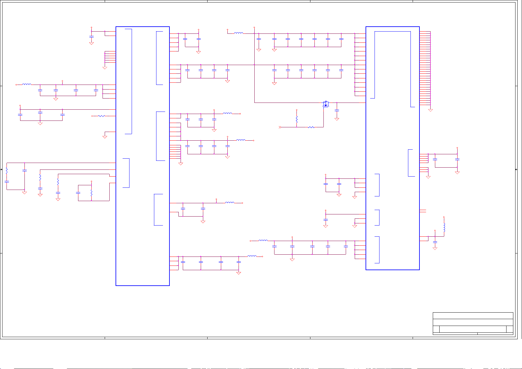
5
U1H
U1H
R8J66977BG
1.8VA_AVD
12
D D
L56
L56
B201212K800TM
B201212K800TM
L0805D
L0805D
1 2
3.3VA
3.3VA_AVDD
12
C C
12
R259
R259
7.5K
7.5K
12
C261
C261
4.7uF/10V/ 0805
4.7uF/10V/ 0805
C0805D
C0805D
B B
C370
C370
0.1uF/10V/ 0402
0.1uF/10V/ 0402
12
C258
C258
0.1uF/10V/ 0402
0.1uF/10V/ 0402
GND
12
10uF/10V/0805
10uF/10V/0805
12
GND
12
12
GND
22nF/25V/0402
22nF/25V/0402
C236
C236
C250
C250
0.1uF/10V/ 0402
0.1uF/10V/ 0402
R260
R260
6.8K/1%/ 0402
6.8K/1%/ 0402
C262
C262
12
C237
C237
0.1uF/10V/ 0402
0.1uF/10V/ 0402
GND
12
12
GND
3.3VA_HDMI
12
C251
C251
0.1uF/10V/ 0402
0.1uF/10V/ 0402
R261
R261
3K/1%/0402
3K/1%/0402
C263
C263
2.2nF/25V/ 0402
2.2nF/25V/ 0402
12
C238
C238
0.1uF/10V/ 0402
0.1uF/10V/ 0402
1.8VA_AVD
12
C266
C266
10nF/25V/0402
10nF/25V/0402
GND
C239
C239
0.1uF/10V/ 0402
0.1uF/10V/ 0402
3.3VA_HDMI
12
C225
C225
0.1uF/10V/ 0402
0.1uF/10V/ 0402
12
R256 0/0402
R256 0/0402
1 2
R262
R262
560/1%/0402
560/1%/0402
R0402D
R0402D
D13
J13
E13
E16
F18
G19
J14
H18
GND
E18
G18
J18
E17
D14
R0402D
R0402D
E15
E14
GND
F21
E21
E22
D18
VDD18HDMI
VDD18HDMI
VSSHDMI
VSSHDMI
VSSHDMI
VSSHDMI
VSSHDMI
VSSHDMI
VDD33HDMI
VDD33HDMI
VDD33_PLL
VDD33_PLL
VDD33IO
VPPOTP
VSSIO
PLL_XFC_A
PLL_XFC_X
PLL_XFC_P
EXT_RES
R8J66977BG
BGA1090-1
BGA1090-1
HDMI
HDMI
4
PLL1AVCC
PLL2AVCC
PLL3AVCC
PLL4AVCC
PLL5AVCC
HDMI Power
HDMI Power
PLL1DVDD
PLL2DVDD
PLL3DVDD
PLL Power
PLL Power
PLL4DVDD
PLL5DVDD
Video ADC Power
Video ADC Power
AVDD33_PLL
AVSS33PLL
Video PLL Power
Video PLL Power
AVDD18
AVDD18
AVDD33
AVDD33
AVDD33
AVDD33
AVDD33
AVSS
AVSS
AVSS
AVSS
AVSS
AVSS18
AVSS18
VDD18
VDD18
VDD18
VDD18
3
1.25VD_C
L55
C246
C246
1 2
C249
C249
10uF/10V/0805
10uF/10V/0805
C0805D
C0805D
3.3VA_AVDD
C255
C255
1 2
12
C369
C369
0.1uF/10V/ 0402
0.1uF/10V/ 0402
L55
B201212K800TM
B201212K800TM
1 2
12
C235
C235
10uF/10V/0805
10uF/10V/0805
GND
L57
L57
B201212K800TM
B201212K800TM
1 2
12
C256
C256
10uF/10V/0805
10uF/10V/0805
C0805D
C0805D
GND
L59
L59
B201212K800TM
B201212K800TM
L0805D
L0805D
1.8VA
L58
L58
B201212K800TM
B201212K800TM
3.3VA
3.3VD
1 2
12
C276
C276
10uF/10V/0805
10uF/10V/0805
C0805D
C0805D
GND
GND
3.3VA
L61 B201212K800TM
L61 B201212K800TM
1 2
L62
L62
B201212K800TM
B201212K800TM
L0805D
L0805D
12
C228
C228
10uF/10V/0805
10uF/10V/0805
CUT_LEAKP4
L0805D
L0805D
1.8VIF
0.1uF/10V/ 0402
0.1uF/10V/ 0402
12
C365
C365
GND
0.1uF/10V/ 0402
0.1uF/10V/ 0402
12
C243
C243
GND
12
C269
C269
10uF/10V/0805
10uF/10V/0805
C0805D
C0805D
CUT_LEAK
12
C313
C313
0.1uF/10V/ 0402
0.1uF/10V/ 0402
12
C364
C364
0.1uF/10V/ 0402
0.1uF/10V/ 0402
3.3V_STB
3.3VD_C
12
C270
C270
0.1uF/10V/ 0402
0.1uF/10V/ 0402
GND
0.1uF/10V/ 0402
0.1uF/10V/ 0402
12
0.1uF/10V/ 0402
0.1uF/10V/ 0402
12
12
R257
R257
10K/0402
10K/0402
C241
C241
C231
C231
R258 100R258 100
1 2
12
C229
C229
0.1uF/10V/ 0402
0.1uF/10V/ 0402
12
C244
C244
0.1uF/10V/ 0402
0.1uF/10V/ 0402
Q37 PMV40UNQ37 PMV40UN
S
12
C271
C271
0.1uF/10V/ 0402
0.1uF/10V/ 0402
0.1uF/10V/ 0402
0.1uF/10V/ 0402
12
0.1uF/10V/ 0402
0.1uF/10V/ 0402
12
G
3.3VD_C
0.1uF/10V/ 0402
0.1uF/10V/ 0402
12
C259
C259
3.3VA_VP
12
C267
C267
0.1uF/10V/ 0402
0.1uF/10V/ 0402
0.1uF/10V/ 0402
0.1uF/10V/ 0402
12
12
C230
C230
0.1uF/10V/ 0402
0.1uF/10V/ 0402
12
C232
C232
0.1uF/10V/ 0402
0.1uF/10V/ 0402
D
12
C252
C252
0.1uF/10V/ 0402
0.1uF/10V/ 0402
GND
12
C260
C260
0.1uF/10V/ 0402
0.1uF/10V/ 0402
GND
C272
C272
0.1uF/10V/ 0402
0.1uF/10V/ 0402
0.1uF/10V/ 0402
0.1uF/10V/ 0402
GND
12
12
12
C226
C226
0.1uF/10V/ 0402
0.1uF/10V/ 0402
12
C233
C233
0.1uF/10V/ 0402
0.1uF/10V/ 0402
12
C247
C247
0.1uF/10V/ 0402
0.1uF/10V/ 0402
12
C253
C253
C264
C264
0.1uF/10V/ 0402
0.1uF/10V/ 0402
C274
C274
10nF/25V/0402
10nF/25V/0402
3.3VD_C 1.25VD
12
C227
C227
0.1uF/10V/ 0402
0.1uF/10V/ 0402
GND
0.1uF/10V/ 0402
0.1uF/10V/ 0402
12
12
C234
C234
0.1uF/10V/ 0402
0.1uF/10V/ 0402
1.8VA_AVD
12
12
C248
C248
0.1uF/10V/ 0402
0.1uF/10V/ 0402
GND
0.1uF/10V/ 0402
0.1uF/10V/ 0402
12
12
C254
C254
0.1uF/10V/ 0402
0.1uF/10V/ 0402
3.3VA_VP
12
C265
C265
10uF/10V/0805
10uF/10V/0805
C0805D
C0805D
GND
12
C275
C275
0.1uF/10V/ 0402
0.1uF/10V/ 0402
P10
N10
P11
P13
T18
V10
N11
V11
N13
N14
E10
E12
C13
C6
D10
E8
D2
C10
D12
E7
D7
D3
E11
E9
H5
J5
J10
J11
J12
J9
2
U1I
U1I
R8J66977BG
R8J66977BG
BGA1090-1
BGA1090-1
L10
VDD12
L11
C242
C242
C245
C245
12
C273
C273
VDD12
L12
VDD12
L13
VDD12
L9
VDD12
M13
VDD12
L14
N18
N19
M20
N20
P9
V6
V8
V16
M14
K4
K5
GND
F5
G5
G4
GNDGND
V13
V15
M4
V18
W10
J2
L5
VDD12
VDD12
VDD12
VDD12
VDD12
VDD12
VDD12
VDD12
VDD12
VDDSTB
VDDA33USB
VDDASSUSB
VDDA33RU
VSSAUSB
AVDD33AUD
AVSS33AUD
AVSS33AUD
VCCQ33
VCCQ33
VCCQ33
VCCQ33
VCCQ33
Core Power
Core Power
USB ANALOG
POWER
USB ANALOG
POWER
Audio DAC
Power
Audio DAC
Power
IO POWER
IO POWER
AB1
VSS
AB9
VSS
M18
VSS
K10
VSS
K11
VSS
K12
VSS
K13
VSS
K14
VSS
K18
VSS
K9
VSS
M10
VSS
M11
VSS
M12
VSS
M5
VSS
M9
VSS
N12
VSS
N9
VSS
P12
VSS
R18
VSS
P3
VSS
P5
VSS
T3
VSS
U18
VSS
U5
VSS
V12
VSS
V17
VSS
V5
VSS
V9
VSS
W4
Core Power
Core Power
VSS
Y3
VSS
Y7
VSS
V14
VSS
Y14
VSS
P14
VSS
GND
E5
MIXVDD33
F4
MIXVDD33
MIXVDD33
MIXVDD33
MIXVDD33
MIXVSS33
MIXVSS33
MIXVSS33
Demodulator ANALOG POWER
Demodulator ANALOG POWER
RESERVED1
RESERVED2
VCC33STB
VCC33STB
12
D1
C257
C257
D5
E4
0.1uF/10V/ 0402
0.1uF/10V/ 0402
E6
F3
D6
GND
D4
C5
R22
L18
3.3VD_ST
12
GND
3.3V_STB
12
C268
C268
0.1uF/10V/ 0402
0.1uF/10V/ 0402
3.3VA_VP
GND
L60
L60
B201212K800TM
B201212K800TM
L0805D
L0805D
12
C371
C371
0.1uF/10V/ 0402
0.1uF/10V/ 0402
1
A A
COMPAL OPTOELECTRONICS CO., LTD
COMPAL OPTOELECTRONICS CO., LTD
COMPAL OPTOELECTRONICS CO., LTD
Title
Title
Title
SCHEMATIC,M/B VTV-L55712,SSC55T
SCHEMATIC,M/B VTV-L55712,SSC55T
SCHEMATIC,M/B VTV-L55712,SSC55T
Size Document Number Rev
Size Document Number Rev
Size Document Number Rev
Custom
Custom
Custom
Date: Sheet of
Wednesday, F ebruary 09, 2011
Date: Sheet of
Wednesday, F ebruary 09, 2011
Date: Sheet of
5
4
3
2
Wednesday, F ebruary 09, 2011
401C41
401C41
401C41
1
11 20
11 20
11 20
1A
1A
1A
Page 41

5
4
3
2
1
Resistor 0402
U20
GND
R1
M9
G9
G7
G3
G1
C9
C7
C3
C1
N1
D2
D8
H2
H8
U20
K4T51163QI-HCE7
K4T51163QI-HCE7
DDR2-H5PS5162FFR-HYNIX
DDR2-H5PS5162FFR-HYNIX
VDD
VDD
J9
VDD
E1
VDD
A1
VDD
VDDQ
VDDQ
VDDQ
VDDQ
E9
VDDQ
VDDQ
VDDQ
VDDQ
VDDQ
A9
VDDQ
J1
VDDL
J2
VREF
A3
VSS
E3
VSS
J3
VSS
VSS
P9
VSS
A7
VSSQ
B2
VSSQ
B8
VSSQ
VSSQ
VSSQ
E7
VSSQ
F2
VSSQ
F8
VSSQ
VSSQ
VSSQ
J7
VSSDL
R8
M8
DRAM_A0
A0
M3
DRAM_A1
A1
M7
DRAM_A2
A2
N2
DRAM_A3
A3
N8
DRAM_A4
A4
N3
DRAM_A5
A5
N7
DRAM_A6
A6
P2
DRAM_A7
A7
P8
DRAM_A8
A8
P3
DRAM_A9
A9
M2
A10
A11
A12
RAS
CAS
ODT
BA1
BA0
CKE
LDM
UDM
LDQS
LDQS
UDQS
UDQS
DQ0
DQ1
DQ2
DQ3
DQ4
DQ5
DQ6
DQ7
DQ8
DQ9
DQ10
DQ11
DQ12
DQ13
DQ14
DQ15
NC1A2NC2
NC3R3NC4R7NC5
E2
DRAM_A10
P7
DRAM_A11
R2
DRAM_A12
K7
DRAM_RAS
L7
DRAM_CAS
K9
DRAM_ODT
L8
DRAM_CS
CS
L1
DRAM_BA2
NC
L3
DRAM_BA1
L2
DRAM_BA0
K3
DRAM_WE
WE
K2
DRAM_CKE
F3
B3
F7
E8
B7
A8
J8
CK
K8
DACLK_N SDCLK_N
CK
G8
G2
H7
H3
H1
H9
F1
F9
C8
C2
D7
D3
D1
D9
B1
B9
DRAM_BA1
DRAM_WE
DRAM_A2
DRAM_CS
DRAM_BA0
DRAM_BA2
DRAM_CKE
DRAM_A1
DRAM_A9
DRAM_A3
DRAM_A7
DRAM_A12
DRAM_A8
DRAM_A11
DRAM_A5
DRAM_A10
DRAM_CAS
DRAM_A0
DRAM_A4
DRAM_A6
DRAM_RAS
12
R277
R277
120/1%/0402
120/1%/0402
1 2
R263 22/1%/0402R263 22/1%/0402
1 2
R267 22/1%/0402R267 22/1%/0402
1 2
R266 22/1%/0402R266 22/1%/0402
1 2
R264 22/1%/0402R264 22/1%/0402
1 2
R268 22/1%/0402R268 22/1%/0402
1 2
R265 22/1%/0402R265 22/1%/0402
1 2
R269 22/1%/0402R269 22/1%/0402
1 2
R270 22/1%/0402R270 22/1%/0402
1 2
R282 22/1%/0402R282 22/1%/0402
1 2
R284 22/1%/0402R284 22/1%/0402
1 2
R283 22/1%/0402R283 22/1%/0402
1 2
R285 22/1%/0402R285 22/1%/0402
1 2
R286 22/1%/0402R286 22/1%/0402
1 2
R288 22/1%/0402R288 22/1%/0402
1 2
R287 22/1%/0402R287 22/1%/0402
1 2
R289 22/1%/0402R289 22/1%/0402
1 2
R292 22/1%/0402R292 22/1%/0402
1 2
R298 22/1%/0402R298 22/1%/0402
1 2
R293 22/1%/0402R293 22/1%/0402
1 2
R301 22/1%/0402R301 22/1%/0402
1 2
R271 22/1%/0402R271 22/1%/0402
1 2
R273 22/1%/0402R273 22/1%/0402
R276 4.7/1%/0402R276 4.7/1%/0402
1 2
R279 4.7/1%/0402R279 4.7/1%/0402
1 2
SDBA1
SDA0
SDWE
SDA1
SDA2
SDA2
SDCS
SDA3
SDA4
SDA5
SDBA0
SDA6
SDBA2
SDA7
SDCKE
SDA8
SDA1
SDA9
SDA10
SDA11
SDA9
SDA12
SDA3
SDA7
SDA12
SDA8
SDA11
SDA5 SDBA2
SDBA1
SDA10
SDBA0
SDODT
SDCAS
SDCKE
SDA0
SDCS
SDA4
SDRAS
SDA6
SDCAS
SDWE
SDRAS
SDODTDRAM_ODT
DADQM0
DADQM1
DADQS0
DADQS0_N
DADQS1
DADQS1_N
SDCLKDACLK
SDDQ0
SDDQ1
SDDQ2
SDDQ3
SDDQ4
SDDQ5
SDDQ6
SDDQ7
SDDQ8
SDDQ9
SDDQ10
SDDQ11
SDDQ12
SDDQ13
SDDQ14
SDDQ15
AB3
AB7
AA4
AA6
AB4
AA8
AA5
AA7
AB6
AB5
AB8
AA2
AB2
AA3
AA1
W7
W5
Y8
Y6
W9
W8
Y4
W6
U3
N3
U2
U1
N2
P1
Y2
V2
U4
W1
W3
V4
W2
T4
V1
R1
R3
R2
P4
R4
T2
N4
P2
SDA0
SDA1
SDA2
SDA3
SDA4
SDA5
SDA6
SDA7
SDA8
SDA9
SDA10
SDA11
SDA12
SDBA2
SDBA1
SDBA0
SDODT
SDCKE
SDCS
SDRAS
SDCAS
SDWE
SDDM0
SDDM1
SDDQS0
SDDQS0_N
SDDQS1
SDDQS1_N
SDCLK
SDCLK_N
SDDQ0
SDDQ1
SDDQ2
SDDQ3
SDDQ4
SDDQ5
SDDQ6
SDDQ7
SDDQ8
SDDQ9
SDDQ10
SDDQ11
SDDQ12
SDDQ13
SDDQ14
SDDQ15
D D
C C
B B
VCCQ18
C282
C282
10uF/10V/0805
10uF/10V/0805
C0805D
C0805D
12
VCCQ18
12
100/1%/0402
100/1%/0402
100/1%/0402
100/1%/0402
12
12
C283 0.1uF/10V/0402C283 0.1uF/10V/0402
C284 0.1uF/10V/0402C284 0.1uF/10V/0402
12
12
C291 0.1uF/10V/0402C291 0.1uF/10V/0402
C290 0.1uF/10V/0402C290 0.1uF/10V/0402
C280 0.1uF/10V/0402C280 0.1uF/10V/0402
VCCQ18
GND
12
12
C286 0.1uF/10V/0402C286 0.1uF/10V/0402
C285 0.1uF/10V/0402C285 0.1uF/10V/0402
12
12
C293 0.1uF/10V/0402C293 0.1uF/10V/0402
C292 0.1uF/10V/0402C292 0.1uF/10V/0402
12
R272
R272
12
R274
R274
12
12
C287 0.1uF/10V/0402C287 0.1uF/10V/0402
C277 0.1uF/10V/0402C277 0.1uF/10V/0402
12
12
C281 0.1uF/10V/0402C281 0.1uF/10V/0402
C294 0.1uF/10V/0402C294 0.1uF/10V/0402
12
C306
C306
0.1uF/10V/0402
0.1uF/10V/0402
12
C307
C307
0.1uF/10V/0402
0.1uF/10V/0402
12
12
C288 0.1uF/10V/0402C288 0.1uF/10V/0402
C289 0.1uF/10V/0402C289 0.1uF/10V/0402
GND
12
12
C279 0.1uF/10V/0402C279 0.1uF/10V/0402
C278 0.1uF/10V/0402C278 0.1uF/10V/0402
GND
U1J
U1J
R8J66977BG
R8J66977BG
BGA1090-1
BGA1090-1
DDR Power
DDR Power
DDR DATA InterfaceDDR ControlDDR Address
DDR DATA InterfaceDDR ControlDDR Address
VCCQ18
VCCQ18
VCCQ18
VCCQ18
VCCQ18
VCCQ18
VCCQ18
VCCQ18
SDVREF0
SDVREF1
DD_CL
VCCQ18
12
12
12
C301 0.1uF/10V/0402C301 0.1uF/10V/0402
C300 0.1uF/10V/0402C300 0.1uF/10V/0402
12
C368 0.1uF/10V/0402C368 0.1uF/10V/0402
GND
12
+
+
C302 0.1uF/10V/0402C302 0.1uF/10V/0402
C303 0.1uF/10V/0402C303 0.1uF/10V/0402
GND
VCCQ18
12
R275
R275
100/1%/0402
100/1%/0402
12
R278
R278
100/1%/0402
100/1%/0402
12
12
C298 0.1uF/10V/0402C298 0.1uF/10V/0402
C299 0.1uF/10V/0402C299 0.1uF/10V/0402
N1
N5
T1
V3
12
12
GND
12
C366 0.1uF/10V/0402C366 0.1uF/10V/0402
GND
12
12
R280
R280
261/1%/0402
261/1%/0402
C367 0.1uF/10V/0402C367 0.1uF/10V/0402
C308
C308
0.1uF/10V/0402
0.1uF/10V/0402
C309
C309
0.1uF/10V/0402
0.1uF/10V/0402
Y1
Y5
Y9
T5
R5
V7
AA9
1 2
L63
L63
B201212K800TM
B201212K800TM
L0805D
L0805D
C304
C304
SE47uF/16V
SE47uF/16V
1.8VD
A A
COMPAL OPTOELECTRONICS CO., LTD
COMPAL OPTOELECTRONICS CO., LTD
COMPAL OPTOELECTRONICS CO., LTD
Title
Title
Title
SCHEMATIC,M/B VTV-L55712,SSC55T
SCHEMATIC,M/B VTV-L55712,SSC55T
SCHEMATIC,M/B VTV-L55712,SSC55T
Size Document Number Rev
Size Document Number Rev
Size Document Number Rev
Custom
Custom
Custom
Date: Sheet of
Wednesday, February 09, 2011
Date: Sheet of
Wednesday, February 09, 2011
Date: Sheet of
5
4
3
2
Wednesday, February 09, 2011
401C41
401C41
401C41
12 20
12 20
12 20
1
1A
1A
1A
Page 42
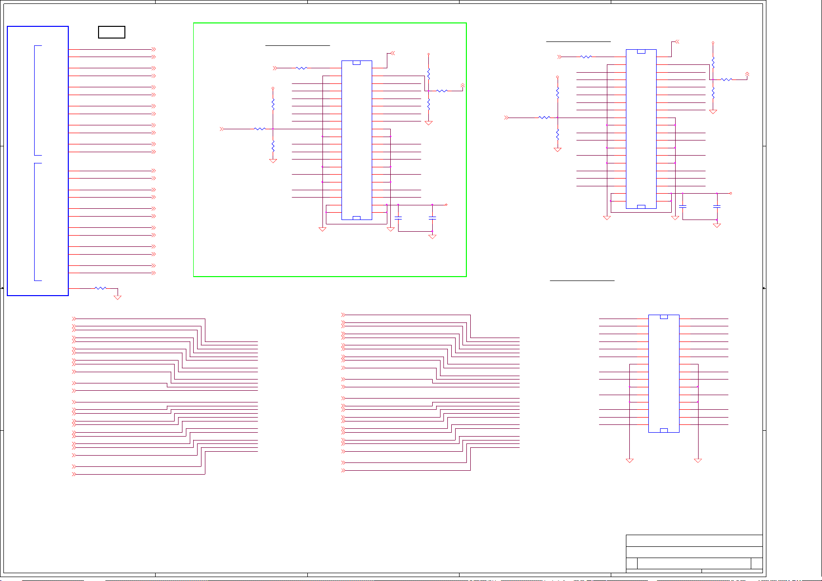
5
U1K
U1K
R8J66977BG
R8J66977BG
BGA1090-1
BGA1090-1
C7 LVDS
AA15
LV1CKOP
AB15
LV1CKOM
AA14
LV1OUT4P
D D
LVDS-ch1LVDS-ch0
LVDS-ch1LVDS-ch0
C C
B B
LV1OUT4M
LV1OUT3P
LV1OUT3M
LV1OUT2P
LV1OUT2M
LV1OUT1P
LV1OUT1M
LV1OUT0P
LV1OUT0M
LV0CKOP
LV0CKOM
LV0OUT4P
LV0OUT4M
LV0OUT3P
LV0OUT3M
LV0OUT2P
LV0OUT2M
LV0OUT1P
LV0OUT1M
LV0OUT0P
LV0OUT0M
TXOUT0M_1P16
TXOUT0P_1P16
TXOUT1M_1P16
TXOUT1P_1P16
TXOUT2M_1P16
TXOUT2P_1P16
TXCLKOUTM_1P16
TXCLKOUTP_1P16
TXOUT3M_1P16
TXOUT3P_1P16
TXOUT4M_1P16
TXOUT4P_1P16
TXOUT0M_2P16
TXOUT0P_2P16
TXOUT1M_2P16
TXOUT1P_2P16
TXOUT2M_2P16
TXOUT2P_2P16
TXCLKOUTM_2P16
TXCLKOUTP_2P16
TXOUT3M_2P16
TXOUT3P_2P16
TXOUT4M_2P16
TXOUT4P_2P16
REFR
AB14
W15
Y15
AA16
AB16
W16
Y16
AA17
AB17
AA12
AB12
AA11
AB11
W11
Y11
W12
Y12
W13
Y13
AA13
AB13
W14
R290 5.6K/1%/0402
R290 5.6K/1%/0402
R0402D
R0402D
1 2
GND
RXCLKINP_2 P16
RXCLKINM_2 P16
RXIN4P_2 P16
RXIN4M_2 P16
RXIN3P_2 P16
RXIN3M_2 P16
RXIN2P_2 P16
RXIN2M_2 P16
RXIN1P_2 P16
RXIN1M_2 P16
RXIN0P_2 P16
RXIN0M_2 P16
RXCLKINP_1 P16
RXCLKINM_1 P16
RXIN4P_1 P16
RXIN4M_1 P16
RXIN3P_1 P16
RXIN3M_1 P16
RXIN2P_1 P16
RXIN2M_1 P16
RXIN1P_1 P16
RXIN1M_1 P16
RXIN0P_1 P16
RXIN0M_1 P16
PANEL_SELP4
TXOUT0M_1
TXOUT0P_1
TXOUT1M_1
TXOUT1P_1
TXOUT2M_1
TXOUT2P_1
TXCLKOUTM_1
TXCLKOUTP_1
TXOUT3M_1
TXOUT3P_1
TXOUT4M_1
TXOUT4P_1
TXOUT0M_2
TXOUT0P_2
TXOUT1M_2
TXOUT1P_2
TXOUT2M_2
TXOUT2P_2
TXCLKOUTM_2
TXCLKOUTP_2
TXOUT3M_2
TXOUT3P_2
TXOUT4M_2
TXOUT4P_2
4
PANEL_SEL
BACKLIGHT_ADJP3,4
R425 0R425 0
1 2
3.3VD
GND
12
R427
R427
10K/0402/NC
10K/0402/NC
12
R423
R423
10K/0402/NC
10K/0402/NC
R424 0/NCR424 0/NC
1 2
RXIN0M_2
RXIN1M_2
RXIN2M_2
RXCLKINM_2
RXIN3M_2
RXIN4M_2
RXIN0M_1
RXIN1M_1
RXIN2M_1
RXCLKINM_1
RXIN3M_1
RXIN4M_1
3
3.3VD
CN17
CN17
A2006WV0-2X20P
A2006WV0-2X20P
39
39
37
35
33
31
292930
272728
252526
232324
212122
191920
171718
151516
131314
111112
9
9
7
7
5
5
3
3
1
1
40
38
36
34
32
10
37
35
33
31
GND
DCR_ADJ P3
P4
DCR_EN
PANEL_SELP4
RXIN0P_2
RXIN1P_2
RXIN2P_2
RXCLKINP_2
RXIN3P_2
RXIN4P_2
RXIN0P_1
RXIN1P_1
RXIN2P_1
RXCLKINP_1
RXIN3P_1
RXIN4P_1
C396
C396
10uF/16V/0805
10uF/16V/0805
12
12
GND
GND
R426
R426
10K/0402/NC
10K/0402/NC
R429 0/NCR429 0/NC
1 2
R421
R421
10K/0402/NC
10K/0402/NC
12
VDD_LCD
C397
C397
0.1uF/10V/0402/NC
0.1uF/10V/0402/NC
40
38
36
34
32
30
28
26
24
22
20
18
16
14
12
10
8
8
6
6
4
4
2
12
2
GND
PANEL_SEL
BACKLIGHT_ADJP3,4
2
R371 0R371 0
1 2
LVDS TX 1-2LVDS Video I/F(Debug)
3.3VD
GND
12
R366
R366
10K/0402/NC
10K/0402/NC
12
R365
R365
10K/0402/NC
10K/0402/NC
R389 0/NCR389 0/NC
1 2
TXOUT4M_2
TXOUT3M_2
TXCLKOUTM_2
TXOUT2M_2
TXOUT1M_2
TXOUT0M_2
TXOUT4M_1
TXOUT3M_1
TXCLKOUTM_1
TXOUT2M_1
TXOUT1M_1
TXOUT0M_1
1
3.3VD
CN15
CN15
A2006WV0-2X20P
A2006WV0-2X20P
39
39
37
35
33
31
292930
272728
252526
232324
212122
191920
171718
151516
131314
111112
9
9
7
7
5
5
3
3
1
1
40
38
36
34
32
10
8
6
4
2
37
35
33
31
GND
DCR_ADJ P3
TXOUT4P_2
TXOUT3P_2
TXCLKOUTP_2
TXOUT2P_2
TXOUT1P_2
TXOUT0P_2
C12
C12
10uF/16V/0805
10uF/16V/0805
12
R391
R391
10K/0402/NC
10K/0402/NC
R390 0/NCR390 0/NC
1 2
12
R392
R392
10K/0402/NC
10K/0402/NC
GND
12
C332
C332
0.1uF/16V/0402/NC
0.1uF/16V/0402/NC
GND
DCR_EN
VDD_LCD
40
38
36
34
32
30
28
26
24
22
20
TXOUT4P_1
18
TXOUT3P_1
16
14
TXCLKOUTP_1
12
10
TXOUT2P_1
8
TXOUT1P_1
6
TXOUT0P_1
4
2
12
GND
LVDS TX 3-4
CN16
CN16
A2006WV0-2X15P
TXOUT0M_3P16
TXOUT0P_3P16
TXOUT1M_3P16
TXOUT1P_3P16
TXOUT2M_3P16
TXOUT2P_3P16
TXCLKOUTM_3P16
TXCLKOUTP_3P16
TXOUT3M_3P16
TXOUT3P_3P16
TXOUT4M_3P16
TXOUT4P_3P16
TXOUT0M_4P16
TXOUT0P_4P16
TXOUT1M_4P16
TXOUT1P_4P16
TXOUT2M_4P16
TXOUT2P_4P16
TXCLKOUTM_4P16
TXCLKOUTP_4P16
TXOUT3M_4P16
TXOUT3P_4P16
TXOUT4M_4P16
TXOUT4P_4P16
TXOUT0M_3
TXOUT0P_3
TXOUT1M_3
TXOUT1P_3
TXOUT2M_3
TXOUT2P_3
TXCLKOUTM_3
TXCLKOUTP_3
TXOUT3M_3
TXOUT3P_3
TXOUT4M_3
TXOUT4P_3
TXOUT0M_4
TXOUT0P_4
TXOUT1M_4
TXOUT1P_4
TXOUT2M_4
TXOUT2P_4
TXCLKOUTM_4
TXCLKOUTP_4
TXOUT3M_4
TXOUT3P_4
TXOUT4M_4
TXOUT4P_4
TXOUT4M_4
TXOUT3M_4 TXOUT3P_4
TXCLKOUTM_4
TXOUT2M_4
TXOUT1M_4
TXOUT0M_4 TXOUT0P_4
TXOUT4M_3
TXOUT3M_3
TXCLKOUTM_3
TXOUT2M_3
TXOUT1M_3
TXOUT0M_3
A2006WV0-2X15P
292930
272728
252526
232324
212122
191920
171718
151516
131314
111112
9
9
7
7
5
5
3
3
1
1
GND GND
30
28
26
24
22
20
18
16
14
12
10
10
8
8
6
6
4
4
2
2
TXOUT4P_4
TXCLKOUTP_4
TXOUT2P_4
TXOUT1P_4
TXOUT4P_3
TXOUT3P_3
TXCLKOUTP_3
TXOUT2P_3
TXOUT1P_3
TXOUT0P_3
P4
A A
COMPAL OPTOELECTRONICS CO., LTD
COMPAL OPTOELECTRONICS CO., LTD
COMPAL OPTOELECTRONICS CO., LTD
Title
Title
Title
SCHEMATIC,M/B VTV-L55712,SSC55T
SCHEMATIC,M/B VTV-L55712,SSC55T
SCHEMATIC,M/B VTV-L55712,SSC55T
Size Document Number Rev
Size Document Number Rev
Size Document Number Rev
C
C
C
Date: Sheet
Date: Sheet
Date: Sheet
Wednesday, February 09, 2011
Wednesday, February 09, 2011
5
4
3
2
Wednesday, February 09, 2011
401C41
401C41
401C41
13 20
13 20
1
13 20
1A
1A
1A
of
of
of
Page 43
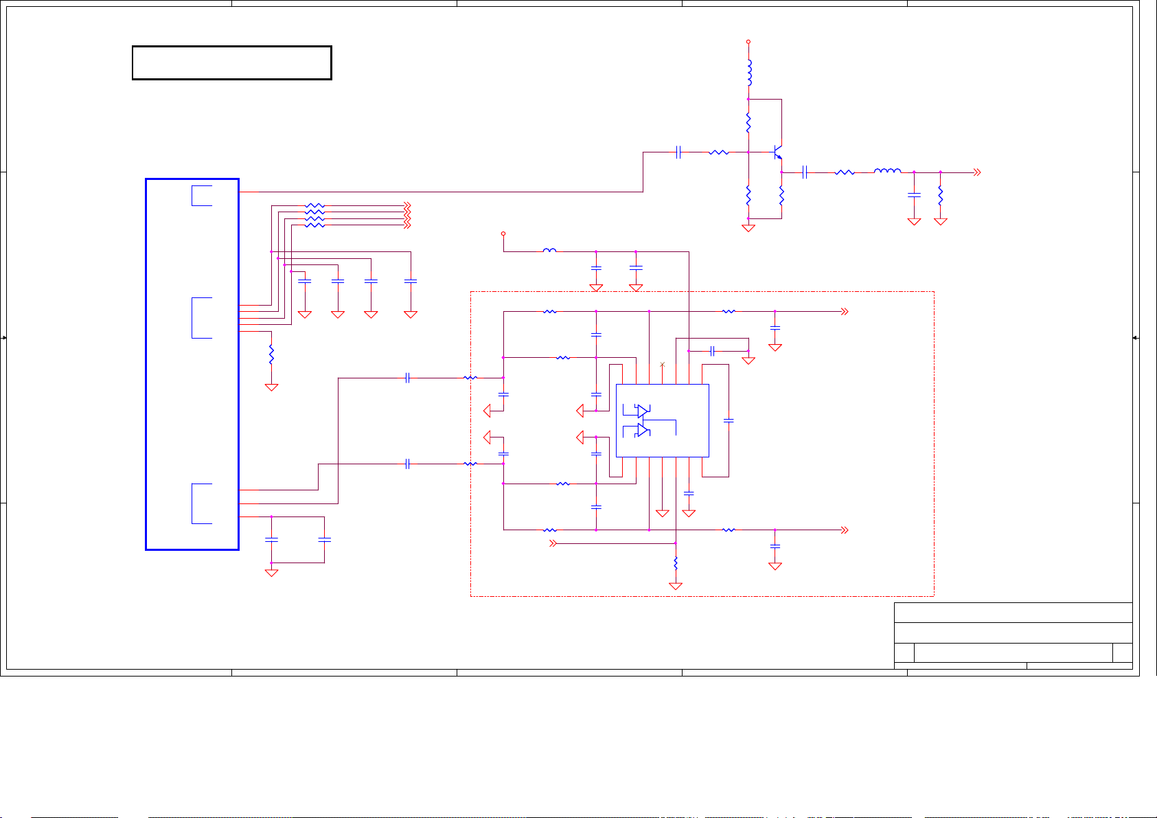
5
SPDIF "Coaxial"
D D
U1L
U1L
R8J66977BG
R8J66977BG
BGA1090-1
BGA1090-1
C C
IIS OUTPUT SPDIF
IIS OUTPUT SPDIF
B B
Audio DAC
Audio DAC
A A
SPDIFO
ADATAO0
BCKO
LRCKO
ACLK
ADATAO1
DA_ROUT
DA_LOUT
DA_VCOM
L2
C7_SPDIF C7_SPDIF
1 2
R322 22/1%/0402R322 22/1%/0402
1 2
R306 22/1%/0402R306 22/1%/0402
1 2
R302 22/1%/0402R302 22/1%/0402
1 2
R321 22/1%/0402R321 22/1%/0402
M2
L1
M1
L3
M3
G2
G1
G3
GND GND GND GND
12
R341
R341
10K/0402
10K/0402
GND
12
C337
C337
10uF/10V/0805
10uF/10V/0805
C0805D
C0805D
GND
12
C110
C110
22pF/50V/0402/NC
22pF/50V/0402/NC
12
4
ADATAO0
BCKO
LRCKO
ACLK
12
12
C112
C111
C111
22pF/50V/0402/NC
22pF/50V/0402/NC
DAC Output
C338
C338
0.1uF/10V/0402
0.1uF/10V/0402
ADATAO0 P15
BCKO P15
LRCKO P15
ACLK P15
12
C113
C113
22pF/50V/0402/NC
22pF/50V/0402/NC
22pF/50V/0402/NC
22pF/50V/0402/NC
C205
C205
4.7uF/10V/0805
4.7uF/10V/0805
C209
C209
4.7uF/10V/0805
4.7uF/10V/0805
R334 15K/1%R334 15K/1%
GND
GND
R300 15K/1%R300 15K/1%
3.3VA
C171
C171
470pF/50V/0402
470pF/50V/0402
C172
C172
470pF/50V/0402
470pF/50V/0402
LINE_MUTEP4
FB67
FB67
KHB0603N121SA
KHB0603N121SA
0.1uF/10V/0402
0.1uF/10V/0402C112
R305 43K/1%R305 43K/1%
R335 43K/1%R335 43K/1%
C158
C158
47pF/50V
47pF/50V
GND
GND
C315
C315
47pF/50V
47pF/50V
R299 43K/1%R299 43K/1%
R291 43K/1%R291 43K/1%
3
C200
C200
C129
C129
GND GND
Line Driver
C168
C168
47pF/50V
47pF/50V
14
INL+
INR+1INR-2OUTR3SGND4EN5PVSS6CN
C170
C170
47pF/50V
47pF/50V
10uF/10V/0805
10uF/10V/0805
12
13
INL-
OUTL
C321
C321
11
NC/UVP
1 2
GND
0.1uF/10V/0402
0.1uF/10V/0402
C206 1uF/16VC206 1uF/16V
9
10
PVDD
PGND
C210
C210
1uF/16V
1uF/16V
GNDGND
R304
R304
10K
10K
R331 2.2KR331 2.2K
1 2
R303 4.7R303 4.7
8
CP
7
R323 4.7R323 4.7
5VSW
12
12
R351
R351
1.5K
1.5K
12
R350
R350
3.3K
3.3K
GND
GND
U14
U14
DRV602PW
DRV602PW
C202
C202
1uF/16V
1uF/16V
L78
L78
B201212K800TM
B201212K800TM
L0805D
L0805D
CE
Q56
Q56
B
MMBT3904L
MMBT3904L
C314
C314
12
R346
R346
220
220
C140
C140
47pF/50V
47pF/50V
GND
C155
C155
47pF/50V
47pF/50V
GND
2
1 2
0.1uF/10V/0402
0.1uF/10V/0402
R349 75/1%R349 75/1%
1 2
LINEOUT_L P6
19" 26" NC
LINEOUT_R P6
L77 KSI0603R56KAL77 KSI0603R56KA
1 2
C326
C326
100pF/25V/0402
100pF/25V/0402
GND
1
R353
R353
100K
100K
SPDIF P6
12
12
GND
COMPAL OPTOELECTRONICS CO., LTD
COMPAL OPTOELECTRONICS CO., LTD
COMPAL OPTOELECTRONICS CO., LTD
Title
Title
Title
SCHEMATIC,M/B VTV-L55712,SSC55T
SCHEMATIC,M/B VTV-L55712,SSC55T
SCHEMATIC,M/B VTV-L55712,SSC55T
Size Document Number Rev
Size Document Number Rev
Size Document Number Rev
Custom
Custom
Custom
Date: Sheet
Wednesday, February 09, 2011
Wednesday, February 09, 2011
Wednesday, February 09, 2011
Date: Sheet
5
4
3
2
Date: Sheet
401C41
401C41
401C41
14 20
14 20
14 20
1
1A
1A
1A
of
of
of
Page 44
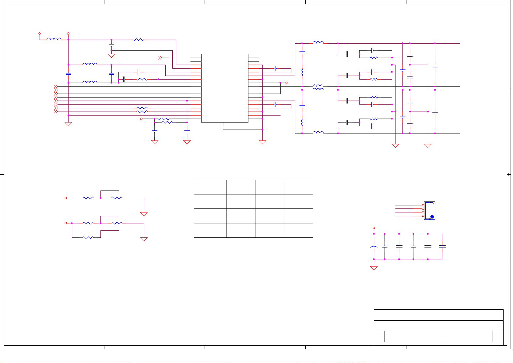
5
4
3
2
1
3.3VD 3.3VD_AU
FB9
FB9
FBMA-300LMT
D D
C C
B B
FBMA-300LMT
FB7
FB7
FBMA-300LMT
FBMA-300LMT
C9
R33
R33
R23
R23
0.1uF/50V
0.1uF/50V
C9
FMT
R34 0R34 0
FS_SEL
R27 10K/0402/N CR27 10K/0402/NC
GAIN_SEL
C8
C8
FB8
0.1uF/50V
0.1uF/50V
ACLKP14
BCKOP14
LRCKOP14
ADATAO0P14
DAMP_RESETNP4
INT_LINEP4
SIDA1P10,18
SICL1P10,18
3.3VD_AU
3.3VD_AU
FB8
FBMA-300LMT
FBMA-300LMT
GND
10K/0402/N C
10K/0402/N C
10K/0402/N C
10K/0402/N C
R29 10K/0402/N CR29 10K/0402/NC
GND
C1
C1
0.1uF/50V
0.1uF/50V
R1 3.3/0805R1 3.3/0805
DAMP_PDNP4
C7 680pF/50VC7 680pF/ 50V
C14
C14
4.7nF/50V
4.7nF/50V
R6 100R6 100
R16 100R16 100
3.3VD_AU
R5
2.2KR52.2K
R21 3.3/0805R21 3.3/0805
GND
GND
U5 S TA333WU5 S TA333W
19
OUT4A
20
OUT4B
21
VDD_DIG
22
VSS_DIG
23
POWRDN
24
VDD_PLL
25
FILTER_PLL
26
GND_PLL
ACLK
BCKO
LRCKO
ADATAO0
DAMP_RESETN
INT_LINE
FS_SEL
GAIN_SEL
C27
C27
0.1uF/50V
0.1uF/50V
GND GND GND
27
XTI
28
BICKI
29
LRCKI
30
SDI
31
RESET
32
INT_LINE
33
SDA
34
SCL
35
GND_DIG
36
VDD_DIG
C28
C28
1nF/50V
1nF/50V
L73,L74
L75,L76
R403,R707
R405,R406
C705,C716
GND_REG
VCC_REG
TEST_MODE
GND_SUB
HEAT_SINK
37
SPEAKER
6 ohm
4.7 ohm 6.2 ohm 12 ohm
0.68 uF 0.47 uF 0.22 uF
18
OUT3A
17
OUT3B
16
CONFIG
15
VDD
14
13
OUT1A
12
GND1
11
VCC1
10
OUT1B
9
OUT2A
8
VCC2
7
GND2
6
OUT2B
5
4
VSS
3
2
SA
1
SPEAKER
8 ohm
15 uH 22 uH 47 uH
2010/12/29 DEL DAMP_GND and parts
C699 0.1uF/50VC699 0.1uF/50V
C712 0.1uF/50VC712 0.1uF/50V
FMT
P_DAMP
SPEAKER
16 ohm
L73
L73
SMTDR75- 15uH /2A
SMTDR75- 15uH /2A
C700
C700
330pF/50V
330pF/50V
R404
R404
22/1206
22/1206
SMTDR75- 15uH /2A
SMTDR75- 15uH /2A
L74
L74
L75
L75
SMTDR75- 15uH /2A
SMTDR75- 15uH /2A
C709
C709
330pF/50V
330pF/50V
R407
R407
22/1206
22/1206
L76
L76
SMTDR75- 15uH /2A
SMTDR75- 15uH /2A
C701
C701
0.1uF/50V
0.1uF/50V
C704
C704
0.1uF/50V
0.1uF/50V
C710
C710
0.1uF/50V
0.1uF/50V
C715
C715
0.1uF/50V
0.1uF/50V
C698 0.1uF/50VC698 0.1uF/50V
R403 4.7/1206R403 4. 7/1206
C703 0.1uF/50VC703 0.1uF/50V
R707 4.7/1206R707 4. 7/1206
R405 4.7/1206R405 4. 7/1206
C713 0.1uF/50VC713 0.1uF/50V
R406 4.7/1206R406 4. 7/1206
C717 0.1uF/50VC717 0.1uF/50V
P_DAMP
C719
C719
SE10uF/35V
SE10uF/35V
C702
C702
1nF/50V
1nF/50V
C708
C708
1nF/50V
1nF/50V
C705 0.68uF/50V/0805C705 0.68uF/50V/0805
C711
C711
1nF/50V
1nF/50V
C718
C718
1nF/50V
1nF/50VR14 10K/0402/NCR14 10K/0402/NC
C716 0.68uF/50V/0805C716 0.68uF/50V/0805
GND GND
SPKER OUT
CN2
CN2
JWT A2001WV2-4P
JWT A2001WV2-4P
C47
C47
0.1uF/50V
0.1uF/50V
SPK_OUTL+
SPK_OUTLSPK_OUTRSPK_OUTR+
C29
C29
1uF/50V/0805
1uF/50V/0805
4
3
2
1
C46
C46
0.1uF/50V
0.1uF/50V
SPK_OUTL+
C706 1nF/50VC706 1nF/50V
SPK_OUTLSPK_OUTR+
C714 1nF/50VC714 1nF/50V
SPK_OUTR-
2mm
2mm
C45
C45
1uF/50V/0805
1uF/50V/0805
C48
C48
0.1uF/50V
0.1uF/50V
GND
A A
COMPAL OPTOELECTRONICS CO., LTD
COMPAL OPTOELECTRONICS CO., LTD
COMPAL OPTOELECTRONICS CO., LTD
Title
Title
Title
SCHEMATIC,M/B VTV-L55712,SSC55T
SCHEMATIC,M/B VTV-L55712,SSC55T
SCHEMATIC,M/B VTV-L55712,SSC55T
Size Document Number Rev
Size Document Number Rev
Size Document Number Rev
Custom
Custom
Custom
Date: Sheet
Date: Sheet
Date: Sheet
Wednesday, February 09, 2011
Wednesday, February 09, 2011
5
4
3
2
Wednesday, February 09, 2011
401C41
401C41
401C41
15 20
15 20
15 20
1
of
of
of
1A
1A
1A
Page 45
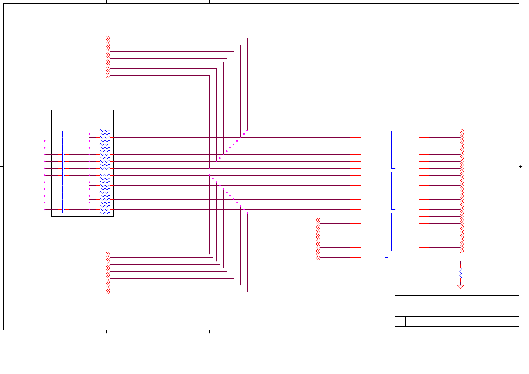
5
RXIN0M_2P13
RXIN0P_2P13
D D
RXIN1M_2P13
RXIN1P_2P13
RXIN2M_2P13
RXIN2P_2P13
RXCLKINM_2P13
RXCLKINP_2P13
RXIN3M_2P13
RXIN3P_2P13
RXIN4M_2P13
RXIN4P_2P13
4
3
2
1
Put close to U1, pcb
C C
B B
A A
trace within 400mil
R2 49.9/1%/0402R2 49.9/1%/0402
C5 0.1uF/10V/0402C5 0.1uF/10V/0402
C42 0.1uF/10V/0402C42 0. 1uF/10V/0402
C76 0.1uF/10V/0402C76 0. 1uF/10V/0402
C44 0.1uF/10V/0402C44 0. 1uF/10V/0402
C2 0.1uF/10V/0402C2 0.1uF/10V/0402
C6 0.1uF/10V/0402C6 0.1uF/10V/0402
C10 0.1uF/10V/0402C10 0. 1uF/10V/0402
C11 0.1uF/10V/0402C11 0. 1uF/10V/0402
C85 0.1uF/10V/0402C85 0. 1uF/10V/0402
C33 0.1uF/10V/0402C33 0. 1uF/10V/0402
C13 0.1uF/10V/0402C13 0. 1uF/10V/0402 R204 49.9/1%/0402R204 49.9/1%/ 0402
R3 49.9/1%/0402R3 49.9/1%/0402
R122 49.9/1%/0402R122 49.9/1%/0402
R50 49.9/1%/ 0402R50 49. 9/1%/0402
R48 49.9/1%/ 0402R48 49. 9/1%/0402
R64 49.9/1%/ 0402R64 49. 9/1%/0402
R80 49.9/1%/ 0402R80 49. 9/1%/0402
R99 49.9/1%/ 0402R99 49. 9/1%/0402
R83 49.9/1%/ 0402R83 49. 9/1%/0402
R127 49.9/1%/0402R127 49.9/1%/0402
R70 49.9/1%/ 0402R70 49. 9/1%/0402
R117 49.9/1%/0402R117 49.9/1%/0402
R119 49.9/1%/0402R119 49.9/1%/0402
R121 49.9/1%/0402R121 49.9/1%/0402
R175 49.9/1%/0402R175 49.9/1%/0402
R177 49.9/1%/0402R177 49.9/1%/0402
R129 49.9/1%/0402R129 49.9/1%/0402
R51 49.9/1%/ 0402R51 49. 9/1%/0402
R120 49.9/1%/0402R120 49.9/1%/0402C87 0.1uF/10V/0402C87 0. 1uF/10V/0402
R123 49.9/1%/0402R123 49.9/1%/0402
R82 49.9/1%/ 0402R82 49. 9/1%/0402
R191 49.9/1%/0402R191 49.9/1%/0402
R135 49.9/1%/0402R135 49.9/1%/0402
RXIN0M_1P13
RXIN0P_1P13
RXIN1M_1P13
RXIN1P_1P13
RXIN2M_1P13
RXIN2P_1P13
RXCLKINM_1P13
RXCLKINP_1P13
RXIN3M_1P13
RXIN3P_1P13
RXIN4M_1P13
RXIN4P_1P13
TXOUT0M_4P13
TXOUT0P_4P13
TXOUT1M_4P13
TXOUT1P_4P13
TXOUT2M_4P13
TXOUT2P_4P13
TXCLKOUTM_4P13
TXCLKOUTP_4P13
TXOUT3M_4P13
TXOUT3P_4P13
TXOUT4M_4P13
TXOUT4P_4P13
U52C
U52C
104
LVDSRXO1N
105
LVDSRXO1P
106
LVDSRXO2N
107
LVDSRXO2P
108
LVDSRXO3N
109
LVDSRXO3P
114
LVDSRXOCLKN
115
LVDSRXOCLKP
116
LVDSRXO4N
117
LVDSRXO4P
118
LVDSRXO5N
119
LVDSRXO5P
122
LVDSRXE1N
123
LVDSRXE1P
124
LVDSRXE2N
125
LVDSRXE2P
126
LVDSRXE3N
127
LVDSRXE3P
132
LVDSRXECLKN
133
LVDSRXECLKP
134
LVDSRXE4N
135
LVDSRXE4P
136
LVDSRXE5N
137
LVDSRXE5P
187
LVDSTXBE1N
188
LVDSTXBE1P
189
LVDSTXBE2N
190
LVDSTXBE2P
191
LVDSTXBE3N
192
LVDSTXBE3P
193
LVDSTXBECLKN
194
LVDSTXBECLKP
196
LVDSTXBE4N
197
LVDSTXBE4P
198
LVDSTXBE5N
199
LVDSTXBE5P
PA131
PA131
LVDSTXAO1N
LVDSTXAO1P
LVDSTXAO2N
LVDSTXAO2P
LVDSTXAO3N
LVDSTXAO3P
LVDSTXAOCLKN
LVDSTXAOCLKP
LVDSTXAO4N
LVDSTXAO4P
LVDSTXAO5N
LVDSTXAO5P
LVDSTXAE1N
LVDSTXAE1P
LVDSTXAE2N
LVDSTXAE2P
LVDSTXAE3N
LVDSTXAE3P
LVDSTXAECLKN
LVDSTXAECLKP
LVDSTXAE4N
LVDSTXAE4P
LVDSTXAE5N
LVDSTXAE5P
LVDSTXBO1N
LVDSTXBO1P
LVDSTXBO2N
LVDSTXBO2P
LVDSTXBO3N
LVDSTXBO3P
LVDSTXBOCLKN
LVDSTXBOCLKP
LVDSTXBO4N
LVDSTXBO4P
LVDSTXBO5N
LVDSTXBO5P
RPI
141
142
143
144
145
146
147
148
150
151
152
153
159
160
161
162
163
164
165
166
168
169
170
171
173
174
175
176
177
178
179
180
182
183
184
185
156
TXOUT0M_1 P13
TXOUT0P_1 P13
TXOUT1M_1 P13
TXOUT1P_1 P13
TXOUT2M_1 P13
TXOUT2P_1 P13
TXCLKOUTM_1 P13
TXCLKOUTP_1 P13
TXOUT3M_1 P13
TXOUT3P_1 P13
TXOUT4M_1 P13
TXOUT4P_1 P13
TXOUT0M_2 P13
TXOUT0P_2 P13
TXOUT1M_2 P13
TXOUT1P_2 P13
TXOUT2M_2 P13
TXOUT2P_2 P13
TXCLKOUTM_2 P13
TXCLKOUTP_2 P13
TXOUT3M_2 P13
TXOUT3P_2 P13
TXOUT4M_2 P13
TXOUT4P_2 P13
TXOUT0M_3 P13
TXOUT0P_3 P13
TXOUT1M_3 P13
TXOUT1P_3 P13
TXOUT2M_3 P13
TXOUT2P_3 P13
TXCLKOUTM_3 P13
TXCLKOUTP_3 P13
TXOUT3M_3 P13
TXOUT3P_3 P13
TXOUT4M_3 P13
TXOUT4P_3 P13
RPI
R251
R251
11.5K/1%
11.5K/1%
GND
COMPAL OPTOELECTRONICS CO., LTD
COMPAL OPTOELECTRONICS CO., LTD
LVDS input
5
4
3
2
COMPAL OPTOELECTRONICS CO., LTD
Title
Title
Title
SCHEMATIC,M/B VTV-L55712,SSC55T
SCHEMATIC,M/B VTV-L55712,SSC55T
SCHEMATIC,M/B VTV-L55712,SSC55T
Size Document Number Rev
Size Document Number Rev
Size Document Number Rev
B
B
B
Date: Sheet
Date: Sheet of
Date: Sheet of
Wednesday, February 09, 2011
Wednesday, February 09, 2011
Wednesday, February 09, 2011
401C41
401C41
401C41
1
of
16 20
16 20
16 20
1A
1A
1A
Page 46

5
4
3
2
1
U52B
U52B
RMDM0
R343 22/1%/0402R343 22/1%/0402
RMDM1
R344 22/1%/0402R344 22/1%/0402
D D
RMDQSP0
R54 22/1%/0402R54 22/1%/0402
RMDQSN0
R46 22/1%/0402R46 22/1%/0402
RMDQSP1
R356 22/1%/0402R356 22/1%/0402
RMDQSN1
R47 22/1%/0402R47 22/1%/0402
MCK_0P
R360 22/1%/0402R360 22/1%/0402
MCK_0N CLKN0
R361 22/1%/0402R361 22/1%/0402
R55 22/1%/0402R55 22/1%/0402
R359 22/1%/0402R359 22/1%/0402
R345 22/1%/0402R345 22/1%/0402
C C
B B
DDRV18
CLKP0
CLKP1
CLKN1
DDR Device PWR
R342 1/0402R342 1/0402
1% 1K
R357 1K/1%R357 1K/1%
1% 1K
1K/1%
1K/1%
DM0
DM1
DQSP0
DQSN0
DQSP1
DQSN1
CKECKERMCKEA
MODT
MRAS
MCS
MCAS
MWE
MA0
MA1
MA2
MA3
MA4
MA5
MA6
MA7
MA8
MA9
MA10
MA11
MA12
MBK0
MBK1
80
MDM0
79
MDM1
83
MDQSP0
84
MDQSN0
87
MDQSP1
88
MDQSN1
57
MCKP0
58
MCKN0
37
MCKP1
38
MCKN1
63
MCKE
32
MODT
33
MRAS
34
MCS
35
MCAS
46
MWE
39
MA0
52
MA1
40
MA2
62
MA3
42
MA4
55
MA5
43
MA6
61
MA7
44
MA8
56
MA9
53
MA10
45
MA11
60
MA12
51
MBANK0
50
MBANK1
V18_VDDLADDRV18
MVREF0
R337
R337
C130
C130
0.1uF/50V
0.1uF/50V
GND
MD0
MD1
MD2
MD3
MD4
MD5
MD6
MD7
MD8
MD9
MD10
MD11
MD12
MD13
MD14
MD15
MVREF
PA131
PA131
97
MD0
70
MD1
99
MD2
68
MD3
67
MD4
100
MD5
71
MD6
96
MD7
91
MD8
76
MD9
93
MD10
73
MD11
74
MD12
94
MD13
77
MD14
90
MD15
MVREF0
65
C88
C88
470pF/50V/0402
470pF/50V/0402
GND
DDRV18
DDRV18
DDRV18
C18
C18
470pF/50V/0402
470pF/50V/0402
C23
C23
0.1uF/10V/0402
0.1uF/10V/0402
C136
C136
470pF/50V/0402
470pF/50V/0402
RMRASnA
RMCSnA
RMCASnA
RAMA0
RAMA2
RAMA4
RAMA6
RAMA8
RAMA11
RMWEnA
RAMBK1
RAMA9
RAMA12
RAMA7
RAMA3
RAMBK0
RAMA1
RAMA10
RAMA5
C19
C19
0.1uF/10V/0402
0.1uF/10V/0402
C24
C24
470pF/50V/0402
470pF/50V/0402
C30
C30
0.1uF/10V/0402
0.1uF/10V/0402
RA122R RA122R
1
2
3
4 5
RA522R RA522R
1
2
3
4 5
RA222R RA222R
1
2
3
4 5
RA322R RA322R
1
2
3
4 5
RA422R RA422R
1
2
3
4 5
C20
C20
470pF/50V/0402
470pF/50V/0402
C25
C25
0.1uF/10V/0402
0.1uF/10V/0402
C128
C128
470pF/50V/0402
470pF/50V/0402
8
7
6
8
7
6
8
7
6
8
7
6
8
7
6
C21
C21
0.1uF/10V/0402
0.1uF/10V/0402
C26
C26
470pF/50V/0402
470pF/50V/0402
C89
C89
0.1uF/10V/0402
0.1uF/10V/0402
R358 100/0402R358 100/0402
MODTRMODTA
MRAS
MCS
MCAS
MA0
MA2
MA4
MA6
MA8
MA11
MWE
MBK1
MA9
MA12
MA7
MA3
MBK0
MA1
MA10
MA5
GND
C22
C22
0.1uF/10V/0402
0.1uF/10V/0402
GND
C31
C31
22uF/10V/1206
22uF/10V/1206
GND
C127
C127
0.1uF/10V/0402
0.1uF/10V/0402
GND
C135
C135
470pF/50V/0402
470pF/50V/0402
MCK_0P
MCK_0N
RMCKEA
RMRASnA
RMCASnA
RMWEnA
RMCSnA
RMODTA
RMDM0
RMDM1
RMDQSP0
RMDQSN0
RMDQSP1
RMDQSN1
RAMA0
RAMA1
RAMA2
RAMA3
RAMA4
RAMA5
RAMA6
RAMA7
RAMA8
RAMA9
RAMA10
RAMA11
RAMA12
RAMBK0
RAMBK1
MVREF0
U4
U4
H5PS5162GFR-S6C
H5PS5162GFR-S6C
J2
Vref
J8
CK
K8
CKn
K2
CKE
K7
RASn
L7
CASn
K3
WEn
L8
CSn
K9
ODT
F3
LDM
B3
UDM
F7
LDQS
E8
LDQQSn
B7
UDQS
A8
UDQSn
M8
A0
M3
A1
M7
A2
N2
A3
N8
A4
N3
A5
N7
A6
P2
A7
P8
A8
P3
A9
M2
A10/AP
P7
A11
R2
A12
L2
BA0
L3
BA1
A2
NC0
E2
NC1
VSSQ0A7VSSQ1B2VSSQ2D2VSSQ3D8VSSQ4E7VSSQ5F2VSSQ6F8VSSQ7H2VSSQ8H8VSSDLJ7VSS0A3VSS1E3VSS2J3VSS3N1VSS4
B8
VSSQ9
P9
VDDQ0
VDDQ1
VDDQ2
VDDQ3
VDDQ4
VDDQ5
VDDQ6
VDDQ7
VDDQ8
VDDQ9
VDDL
VDD0
VDD1
VDD2
VDD3
VDD4
DQ0
DQ1
DQ2
DQ3
DQ4
DQ5
DQ6
DQ7
DQ8
DQ9
DQ10
DQ11
DQ12
DQ13
DQ14
DQ15
NC2
NC3
NC4
NC5
DDRV18
C1
C3
C7
C9
V18_VDDLA
E9
G1
G3
G7
G9
A9
J1
A1
E1
J9
M9
R1
G8
G2
H7
H3
H1
H9
F1
F9
C8
C2
D7
D3
D1
D9
B1
B9
L1
R3
R7
R8
DDRV18
MMD0
MMD1
MMD2
MMD3
MMD4
MMD5
MMD6
MMD7
MMD8
MMD9
MMD10
MMD11
MMD12
MMD13
MMD14
MMD15
V18_VDDLA
C15
C15
470pF/50V/0402
470pF/50V/0402
GND
MD6
MD1
MD3
MD4
MD14
MD9
MD12
MD11
MD5
MD2
MD0
MD7
MD13
MD10
MD8
MD15
C16
C16
0.1uF/10V/0402
0.1uF/10V/0402
1
2
3
4 5
1
2
3
4 5
1
2
3
4 5
1
2
3
4 5
RA622R RA622R
RA722R RA722R
RA822R RA822R
RA922R RA922R
C17
C17
1uF/6.3V/0402
1uF/6.3V/0402
8
7
6
8
7
6
8
7
6
8
7
6
MMD6
MMD1
MMD3
MMD4
MMD14
MMD9
MMD12
MMD11
MMD5
MMD2
MMD0
MMD7
MMD13
MMD10
MMD8
MMD15
A A
COMPAL OPTOELECTRONICS CO., LTD
COMPAL OPTOELECTRONICS CO., LTD
COMPAL OPTOELECTRONICS CO., LTD
Title
Title
Title
SCHEMATIC,M/B VTV-L55712,SSC55T
SCHEMATIC,M/B VTV-L55712,SSC55T
SCHEMATIC,M/B VTV-L55712,SSC55T
Size Document Number Rev
Size Document Number Rev
Size Document Number Rev
Custom
Custom
Custom
Date: Sheet of
Wednesday, February 09, 2011
Date: Sheet of
Wednesday, February 09, 2011
Date: Sheet of
5
4
3
2
Wednesday, February 09, 2011
401C41
401C41
401C41
17 20
17 20
17 20
1
0
0
0
Page 47
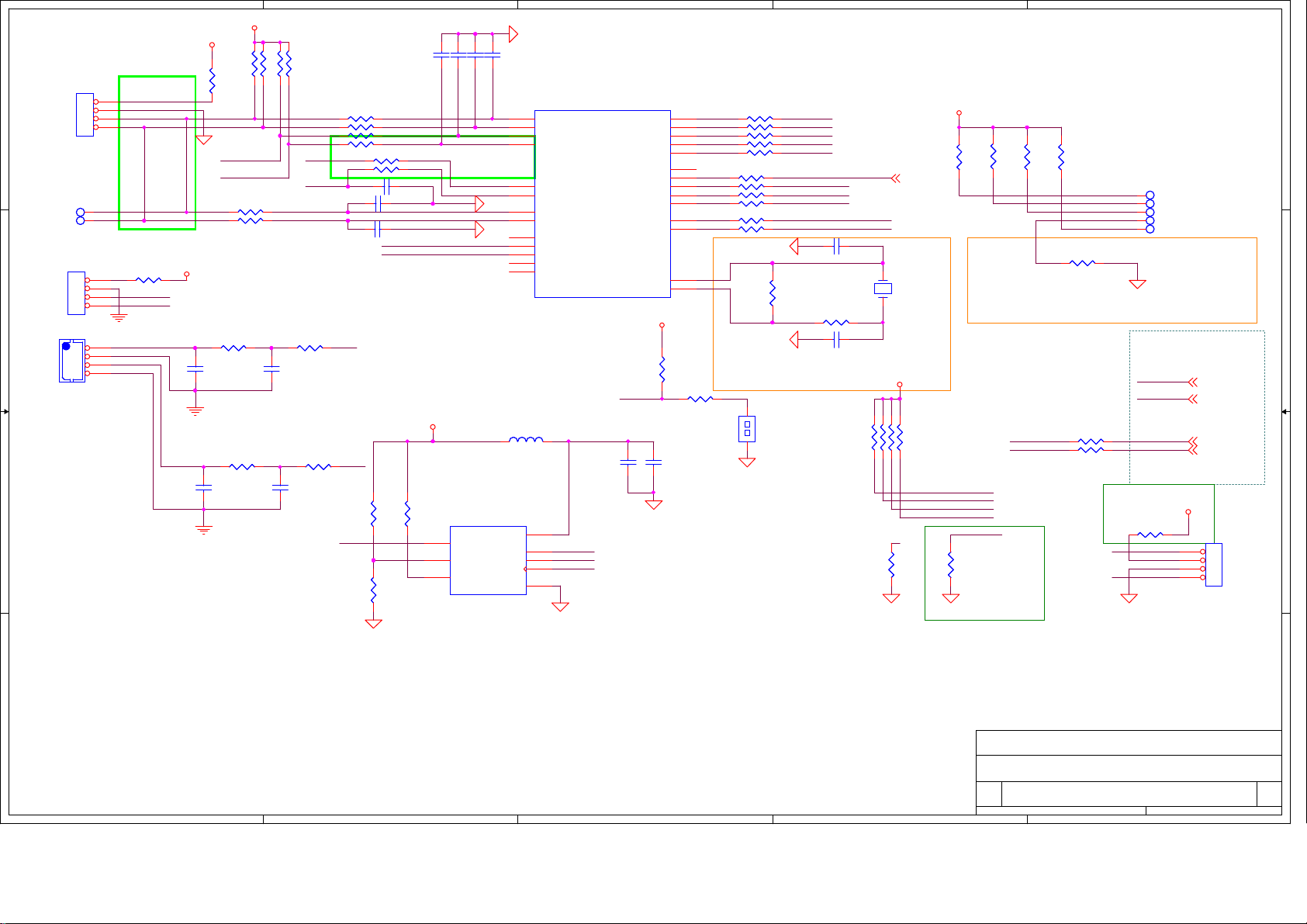
5
V33
V33
R9210K/NC R9210K/ NC
R7910K/NC R7910K/ NC
R3984.7K/0402 R3984.7K/0402
R3934.7K/0402 R3934.7K/0402
R660R66
V33
C340
C340
C399
C399
GND
0
M_SICL1
M_SIDA1
R90 100R90 100
R374 100R374 100
R428
R428
C339
C339
1K/0402/NC
1K/0402/NC
0.1uF/10V/0402/NC
0.1uF/10V/0402/NC
R431
R431
C398
C398
1K/0402/NC
1K/0402/NC
0.1uF/10V/0402/NC
0.1uF/10V/0402/NC
R74 100/0402R74 100/0402
R384 100/0402R384 100/0402
R91 100/0402R91 100/0402
R78 100/0402R78 100/0402
2010 / 12/ 16 R383 change to 1K
TESTEN
RSTn
R422
R422
PWM0
1K/0402/NC
1K/0402/NC
R430
R430
PWM1
1K/0402/NC
1K/0402/NC
10K/0402
10K/0402
J4
J4
1
D D
C C
JWT A2001WV2-4P
JWT A2001WV2-4P
JWT A2001WV2-4P/NC
JWT A2001WV2-4P/NC
B B
2
3
4
JWT A2001WV2-4P
JWT A2001WV2-4P
TP24TP24
TP27TP27
2010/12/20 High speed for PQ function,
R90 R374 from NC to 100
2-Wire Master
J3
J3
1
2
3
4
1
2mm
2mm
2
3
4
CN4
CN4
SCL_S
SDA_S
SDA_S
INTL
INTH
R118 0R118 0
M_SICL1
M_SIDA1
1uF/6.3V/0402/NC
1uF/6.3V/0402/NC
1uF/6.3V/0402/NC
1uF/6.3V/0402/NC
4
GND
C1833.3pF/ 25V/0402 C1833.3pF/25V/0402
C1523.3pF/ 25V/0402 C1523.3pF/25V/0402
C1823.3pF/ 25V/0402 C1823.3pF/25V/0402
R85 0R85 0
R383 1KR383 1K
C151 0.1uF/10V/0402C151 0.1uF/10V/0402
C345 3.3pF/50V/NCC345 3.3pF/50V/NC TP25TP25
C201 3.3pF/50V/NCC201 3.3pF/50V/NC
PWM0
PWM1
V33
R394
R394
SPICS0
R396
R396
10K/0402
10K/0402
U9
U9
1
3
7
MX25L8006EM2I-12G
MX25L8006EM2I-12G
GND
R130
R130
10K/0402/NC
10K/0402/NC
nCE
nWP
nHOLD
C3413.3pF/ 25V/0402 C3413.3pF/25V/0402
U52A
U52A
2
3
21
20
4
5
GND
12
15
GND
17
18
19
22
23
PA131
PA131
L18 B201212K800TM
L18 B201212K800TM
L0805D
L0805D
1 2
8
VCC
2
SO
5
SI
6
SCK
4
GND
TWOWSCL0
TWOWSDA0
TWOWSCL1
TWOWSDA1
TESTEN
RESETN
IINTL
INTH
GPIO4
GPIO5
GPIO6
GPIO9
GPIO10
0.1uF/10V/0402
0.1uF/10V/0402
SPIRXD
SPITXD
SPICLK
GND
C342
C342
3
TDI
TMS
TCK
TRSTN
TDO
SPICS1
SPICS0
SPICLK
SPITXD
SPIRXD
UARTRXD0
UARTTXD0
XIN
XOUT
R399
R399
4.7K/0402
4.7K/0402
RSTn
GND
V33
C349
C349
10uF/6.3V
10uF/6.3V
8
R387 0R387 0
9
R77 0R77 0
10
R81 0R81 0
7
R87 0R87 0
11
R382 0R382 0
29
24
R84 0R84 0
25
R86 0R86 0
26
R88 0R88 0
28
R89 0R89 0
13
R408 0R408 0
16
R388 0R388 0
207
208
2010/12/23 C343 18p to 27p; C344 18p
to 22p; R418 1K to 220
R401100/0402 R401100/0402
PA_TDI
PA_TMS
PA_TCK
PA_TRST
PA_TDO
SPICS0
SPICLK
SPITXD
SPIRXD
U_RX0
U_TX0
C343 27pF/50V/0402C343 27pF/50V/0402
GND
R386
R386
2.2M
2.2M
220/1%
220/1%
R418
R418
GND
C344 22pF/50V/0402C344 22pF/50V/0402
J2
J2
JWT A2003WV0-1X2
JWT A2003WV0-1X2
1 2
GND
2
V33
R114
R114
R400
R400
10K/0402
10K/0402
10K/0402
TM0
TM1
TM2
TM3
10K/0402
2010/11/16 pixelworks suggest form 0 to 10K
M_SICL1
M_SIDA1
INTL
U_RX0
INTH
U_TX0
SPICS0
R373
R373
Bootstrap:
0: Normal,
1: Flash
10K/0402/NC
10K/0402/NC
SPICS0 P4
X2
X2
27.0MHz/18pF/S/2P
27.0MHz/18pF/S/2P
1 2
V33
R39710K/0402/NC R39710K/0402/N C
R37210K/0402 R37210K/0402
R38110K/0402/NC R38110K/0402/N C
R39510K/0402 R39510K/0402
TESTEN
R402
R402
0/0402
0/0402
2010/12/15 10K change to NC
R364
R364
R385
R385
10K/0402
10K/0402
10K/0402
10K/0402
R362 10KR362 10K
R419 0R419 0
R420 0R420 0
PA_TCK
PA_TDO
PA_TMS
PA_TRST
PA_TDI
GND
to SoC (MCU)
RSTn
SPICS0
SICL1
SIDA1
R363 0/NCR363 0/ NC
U_TX0
U_RX0
GNDGNDGND
2011/1/5 0 change to NC
1
TP29TP29
TP30TP30
TP28TP28
TP26TP26
RSTn P4
SPICS0 P4
SICL1 P10,15
SIDA1 P10,15
V33
J5
J5
1
2
3
4
JWT A2001WV2-4P
JWT A2001WV2-4P
A A
COMPAL OPTOELECTRONICS CO., LTD
COMPAL OPTOELECTRONICS CO., LTD
COMPAL OPTOELECTRONICS CO., LTD
Title
Title
Title
SCHEMATIC,M/B VTV-L55712,SSC55T
SCHEMATIC,M/B VTV-L55712,SSC55T
SCHEMATIC,M/B VTV-L55712,SSC55T
Size Document Number Rev
Size Document Number Rev
Size Document Number Rev
B
B
B
Date: Sheet
Date: Sheet of
Date: Sheet of
Wednesday, February 09, 2011
Wednesday, February 09, 2011
5
4
3
2
Wednesday, February 09, 2011
401C41
401C41
401C41
1
of
18 20
18 20
18 20
0
0
0
Page 48

5
4
3
2
1
0.1uF/10V/0402
0.1uF/10V/0402
C377
C377
470pF/50V/0402
470pF/50V/0402
L5
L5
B201212K800TM
B201212K800TM
1 2
LPLLVDD1V
85
139
LPLLVDD1V
VDDDLL1V_1
1.0V
1.0V
LPLLVSS
138
VDDDLL1V
C114
C114
C107
C107
470pF/50V/0402
470pF/50V/0402
C123
C123
0.1uF/10V/0402
0.1uF/10V/0402
LVRAVDD1V
1
130
112
VDD1V_1
LVRAVDD1V_2
LVRAVDD1V_1
LVRAVSS2
LVRAVSS1
129
111
C124
C124
470pF/50V/0402
470pF/50V/0402
0.1uF/10V/0402
0.1uF/10V/0402
L6
L6
B201212K800TM
B201212K800TM
1 2
VDD1V
102
103
30
154
VDD1V_348VDD1V_482VDD1V_5
VDD1V_6
VDD1V_2
C375
C375
10uF/6.3V
10uF/6.3V
C125
C125
V10
200
201
VDD1V_7
VDD1V_8
VDD1V_9
LVRAVDD1V
C94
C94
0.1uF/10V/0402
0.1uF/10V/0402
0.1uF/10V/0402
0.1uF/10V/0402
C131
C131
C134
C134
10uF/6.3V
10uF/6.3V
10uF/6.3V
10uF/6.3V
GND
VDDM DDRV18
R416
R416
R409
R409
R414
R414
0/0402
0/0402
0/0402
0/0402
0/0402
0/0402
R412
R412
0/0402
0/0402
VDD1V
VDDM VDDIO
59
31
VDDM_249VDDM_3
VDDM_141VDDM_466VDDM_572VDDM_678VDDM_786VDDM_892VDDM_9
VDDM_0
VSSM247VSSM354VSSM464VSSM569VSSM675VSSM781VSSM889VSSM995VSSM10
VSSM1
36
4
C362
C362
98
101
C77
C116
C116
1uF/6.3V/0402
1uF/6.3V/0402
C133
C133
1uF/6.3V/0402
1uF/6.3V/0402
C77
470pF/50V/0402
470pF/50V/0402
VPOR3V3 LVRPLLVDD3V3
C373
C373
0.1uF/10V/0402
0.1uF/10V/0402
GND GND
V33
R4110/0402 R4110/0402
470pF/50V/0402
470pF/50V/0402
VDDIO
27
202
VDDIO_16VDDIO_214VDDIO_3
VDDIO_4/PLLIO
C79
C79
C80
C80
470pF/50V/0402
470pF/50V/0402
0.1uF/10V/0402
0.1uF/10V/0402
0.1uF/10V/0402
0.1uF/10V/0402
AVDDIO
LVRVDD
113
131
LVRVDD1
LVRVDD2
3.3V1.8V
3.3V1.8V
LVRVSS1
LVRVSS2
LVRPLLVSS
110
128
121
VDD1V
0.1uF/10V/0402
0.1uF/10V/0402
C139
C139
C383
C383
C358
C358
0.1uF/10V/0402
0.1uF/10V/0402
GND
LVRPLLVDD3V3
AVDDIO
140
149
158
120
AVDDIO_1
AVDDIO_2
LVRPLLVDD3V3
3
C382
C382
C360
C360
1uF/6.3V/0402
1uF/6.3V/0402
470pF/50V/0402
470pF/50V/0402
167
172
181
AVDDIO_3
AVDDIO_4
AVDDIO_5
C81
C81
470pF/50V/0402
470pF/50V/0402
0.1uF/10V/0402
0.1uF/10V/0402
C391
C391
VPOR3V3
186
157
195
VPOR3V3
AVDDIO_6
AVDDIO_7
AVDDIO_8
VPORVSS
155
GND
C82
C82
0.1uF/10V/0402
0.1uF/10V/0402
C363
C363
C380
C380
0.1uF/10V/0402
0.1uF/10V/0402
C117
C117
0.1uF/10V/0402
0.1uF/10V/0402
470pF/50V/0402
470pF/50V/0402
EPAD/GND
209
C83
C83
470pF/50V/0402
470pF/50V/0402
C352
C352
1uF/6.3V/0402
1uF/6.3V/0402
C384
C384
LVRVDD
C84
C84
C355
C355
470pF/50V/0402
0.1uF/10V/0402
0.1uF/10V/0402
C96
C96
0.1uF/10V/0402
0.1uF/10V/0402
V33A
470pF/50V/0402
C374
C374
C149
C149
10uF/6.3V
10uF/6.3V
470pF/50V/0402
470pF/50V/0402
GND GND
C392
C392
470pF/50V/0402
470pF/50V/0402
R4150 R4150
L10
L10
1 2
B201212K800TM
B201212K800TM
2
C122
C122
0.1uF/10V/0402
0.1uF/10V/0402
C150
C150
0.1uF/10V/0402
0.1uF/10V/0402
C98
C98
0.1uF/10V/0402
0.1uF/10V/0402
470pF/50V/0402
470pF/50V/0402
LVRPLLVDD3V3
VDDIOLVRVDD
C393
C361
C361
470pF/50V/0402
470pF/50V/0402
C350
C350
470pF/50V/0402
470pF/50V/0402
C99
C99
COMPAL OPTOELECTRONICS CO., LTD
COMPAL OPTOELECTRONICS CO., LTD
COMPAL OPTOELECTRONICS CO., LTD
Title
Title
Title
Size Document Number Rev
Size Document Number Rev
Size Document Number Rev
B
B
B
Date: Sheet
Date: Sheet of
Date: Sheet of
C393
22uF/10V/1206
22uF/10V/1206
GND
C351
C381
C381
0.1uF/10V/0402
0.1uF/10V/0402
470pF/50V/0402
470pF/50V/0402
C101
C101
22uF/10V/1206
22uF/10V/1206
AVDDIO VPOR3V3
SCHEMATIC,M/B VTV-L55712,SSC55T
SCHEMATIC,M/B VTV-L55712,SSC55T
SCHEMATIC,M/B VTV-L55712,SSC55T
Wednesday, February 09, 2011
Wednesday, February 09, 2011
Wednesday, February 09, 2011
C359
C359
V33A
C353
C353
0.1uF/10V/0402
0.1uF/10V/0402
R4100 R4100
401C41
401C41
401C41
C351
470pF/50V/0402
470pF/50V/0402
L8
L8
B201212K800TM
B201212K800TM
1
C354
C354
1uF/6.3V/0402
1uF/6.3V/0402
12
of
19 20
19 20
19 20
1A
1A
1A
C390
C390
1uF/6.3V/0402
1uF/6.3V/0402
VDDM
C120
C120
470pF/50V/0402
470pF/50V/0402
0.1uF/10V/0402
0.1uF/10V/0402
VDDDLL1V
L19
L19
B201212K800TM
B201212K800TM
1 2
DPLLVDD1V
U52D
U52D
PA131
PA131
LPLLVDD1V
C132
C132
470pF/50V/0402
470pF/50V/0402
C121
C121
LPLLVDD1V LVRAVDD1V
VDDDLL1V
203
205
DPLLVDD1V
MPLLVDD 1V
PLLVSS1
PLLVSS2
204
206
DPLLVDD1V
C106
C103
C103
1uF/6.3V/0402
1uF/6.3V/0402
D D
C389
C389
470pF/50V/0402
470pF/50V/0402
0.1uF/10V/0402
0.1uF/10V/0402
C C
B201212K800TM
B201212K800TM
B B
A A
C106
470pF/50V/0402
470pF/50V/0402
GND GND GND G ND
470pF/50V/0402
C119
C119
0.1uF/10V/0402
0.1uF/10V/0402
DPLLVDD1V
1 2
MPLLVDD1V
C126
C126
1uF/6.3V/0402
1uF/6.3V/0402
470pF/50V/0402
C118
C118
L20
L20
B201212K800TM
B201212K800TM
1 2
MPLLVDD1V
C357
C357
470pF/50V/0402
470pF/50V/0402
GND
5
C115
C115
MPLLVDD1V
L21
L21
Page 49
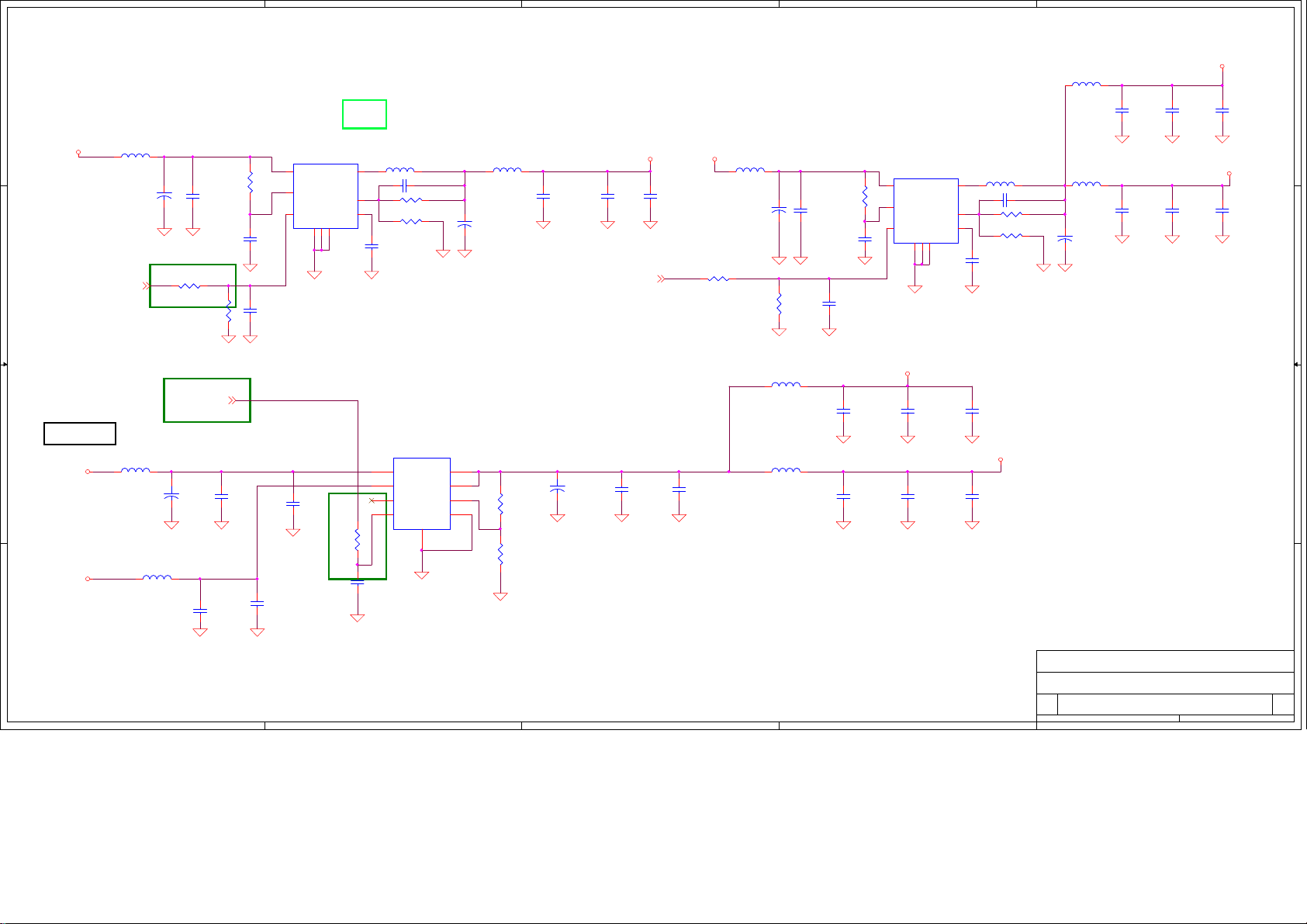
5
4
3
2
1
12
C755
C755
10nF/25V/0402
10nF/25V/0402
12
C749
C749
10nF/25V/0402
10nF/25V/0402
V33A
12
C756
C756
0.1uF/10V/0402
0.1uF/10V/0402
V33
12
C750
C750
0.1uF/10V/0402
0.1uF/10V/0402
of
of
of
20 20
20 20
20 20
1A
1A
1A
B201212K800TM
B201212K800TM
L29
L29
L0805D
L0805D
1 2
D D
DC - DC FROM VCC TO 1.08V(3A)
L33 B201212K800TM
L33 B201212K800TM
P5V
2010/12/20 Change R749 100K to 47K
C C
3.3V -> 1.8V
B B
V33A
P5V
A A
L0805D
L0805D
1 2
C723
C723
10uF/10V/0805
10uF/10V/0805
GND
POWER_ON3P4
2010/12/20 Change input form pin5 to Power on
L31 B201212K800TM
L31 B201212K800TM
L0805D
L0805D
1 2
L37 B201212K800TM
L37 B201212K800TM
L0805D
L0805D
1 2
5
PA131 V10 (0.93V~1.2V)
C724
C724
0.1uF/10V/0402
0.1uF/10V/0402
0.1uF/10V/0402
0.1uF/10V/0402
GND
R749 47K/1%/0402R749 47K/1%/0402
1 2
R752
R752
20K/1%/0402/NC
20K/1%/0402/NC
POWER_ON3P4
C736
C736
+
+
SE100uF/16V
SE100uF/16V
12
C759
C759
0.1uF/10V/0402
0.1uF/10V/0402
R743
R743
C729
C729
1 2
GND
12
C740
C740
0.1uF/10V/0402
0.1uF/10V/0402
GND
10/0402
10/0402
GND
GND
12
GNDGND
C734
C734
1uF/16V
1uF/16V
C0603D
C0603D
12
C758
C758
1uF/16V
1uF/16V
C0603D
C0603D
U49
U49
G5694
G5694
8
VIN
1
VCC
5
EN
6
GND
PGND
3
GND
FB
REF
THEM_PAD
9
GND
7
LX
4
2
Vout=0.8Vx (1+R1/R2)
12
C741
C741
1uF/16V
1uF/16V
C0603D
C0603D
GND
10K/0402
10K/0402
1uF/16V
1uF/16V
C0603D
C0603D
C735
C735
R758
R758
12
12
GND
L22 2.2uH/3.8AL22 2.2uH/3.8A
C722 47pF/50V/0402C722 47pF/50V/0402
R744 5.6K/1%R744 5.6K/1%
R746 16K/1%R746 16K/1%
C730
C730
0.1uF/10V/0402
0.1uF/10V/0402
GND
U51
U51
AX6615
AX6615
5
6
7
8
VO
VIN
VO
VPP
ADJ
POK
GND
VEN
ThPad
9
GND
2010/12/20 47K to 10K
4
C726
C726
PVM330uF/6V
PVM330uF/6V
GND
4
3
2
1
L30 B201212K800TM
L30 B201212K800TM
L0805D
L0805D
1 2
10uF/10V/0805
10uF/10V/0805
GND
12
C745
C745
C0805D
C0805D
10nF/25V/0402
10nF/25V/0402
12
C747
C747
POWER_ON3P4
G5694 EN: ON=2V, OFF=0.4V
12
10nF/25V/0402
10nF/25V/0402
GND
1 2
1 2
R755
R755
12.7K/1%
12.7K/1%
R757
R757
10K/1%
10K/1%
+
+
GND
C739
C739
PVM330uF/6V
PVM330uF/6V
C737
C737
V10
12
C746
C746
0.1uF/10V/0402
0.1uF/10V/0402
GNDGND
3
R756 10K/1%/0402R756 10K/1%/0402
12
C738
C738
0.1uF/10V/0402
0.1uF/10V/0402
GNDGND
DC - DC FROM VCC TO 3.3V(2A)
P5V
B201212K800TM
B201212K800TM
L36
L36
L0805D
L0805D
1 2
20K/1%/0402/NC
20K/1%/0402/NC
1 2
C727
C727
10uF/10V/0805
10uF/10V/0805
R751
R751
C728
C728
0.1uF/10V/0402
0.1uF/10V/0402
0.1uF/10V/0402
0.1uF/10V/0402
GND
1 2
GND
L35 B201212K800TM
L35 B201212K800TM
L0805D
L0805D
1 2
L34 B201212K800TM
L34 B201212K800TM
L0805D
L0805D
1 2
R745
R745
10/0402
10/0402
C732
C732
GNDGND
12
C751
C751
0.1uF/10V/0402
0.1uF/10V/0402
GND
12
C753
C753
10uF/10V/0805
10uF/10V/0805
C0805D
C0805D
GND GNDGND
12
C742
C742
10uF/10V/0805
10uF/10V/0805
C0805D
C0805D
GNDGND GNDGND
8
1
5
U50
U50
G5694
G5694
VIN
VCC
EN
GND
6
PGND
3
GND
THEM_PAD
9
LX
FB
REF
Vout=0.8Vx (1+R1/R2)
DDRV18
12
C754
C754
10nF/25V/0402
10nF/25V/0402
12
C743
C743
10nF/25V/0402
10nF/25V/0402
2
B201212K800TM
B201212K800TM
L25
L25
L0805D
L32 2.2uH/3.8AL32 2.2uH/3.8A
7
C725 47pF/50V/0402C725 47pF/50V/0402
4
R747 49.9K/1%R747 49.9K/1%
2
R748 16K/1%R748 16K/1%
C733
C733
0.1uF/10V/0402
0.1uF/10V/0402
GND
1 2
C731
C731
PVM330uF/6V
PVM330uF/6V
GNDGND
L0805D
DDR Device---MV18(1.69V~1,9V)
12
C752
C752
0.1uF/10V/0402
0.1uF/10V/0402
VDDM
PA131 DDR IO---PV18(1.69V~1.9V)
2010 11 18_CHANGE PV18 TO VDDM
12
C744
C744
0.1uF/10V/0402
0.1uF/10V/0402
COMPAL OPTOELECTRONICS CO., LTD
COMPAL OPTOELECTRONICS CO., LTD
COMPAL OPTOELECTRONICS CO., LTD
Title
Title
Title
SCHEMATIC,M/B VTV-L55712,SSC55T
SCHEMATIC,M/B VTV-L55712,SSC55T
SCHEMATIC,M/B VTV-L55712,SSC55T
Size Document N um ber Rev
Size Document N um ber Rev
Size Document N um ber Rev
Custom
Custom
Custom
Date: Sheet
Date: Sheet
Date: Sheet
Wednesday, February 09, 2011
Wednesday, February 09, 2011
Wednesday, February 09, 2011
12
C757
C757
10uF/10V/0805
10uF/10V/0805
C0805D
C0805D
GND GNDGND
12
C748
C748
10uF/10V/0805
10uF/10V/0805
C0805D
C0805D
GND GNDGND
401C41
401C41
401C41
1
Page 50

SCHEMATIC DIAGRAM
POWER
55”(P554410-00)
Page 51

1
2
3
4
5
6
7
8
S1
R218
:7000P-0106
+
C219
C216
S2
12Va/1.72A
12Va
24Vi/10.8A
24Vi
12Vcc/1.0A
12Vcc
GND
P802
16
15
14
13
12
11
10
9
8
7
6
5
4
3
2
P803
14
13
12
11
10
9
8
7
6
5
4
3
2
1
P804
14
13
12
11
10
9
8
7
6
5
4
3
2
1
size:A2 rev: 0
DESIGNER:
Sheet of11
8
L203
S2
! !
P801
F101
L
A A
P801:1P801:3
CY105
CY106
N
B B
!
TH101
LF103:1
1 2
R101
VA101
!
!
LF103:2
+
C611
C604
R625
!
R626
L602:7
C C
!
L602:12
B+
R606 R607 R608 R609 R610
D D
1
!
!
!
34
C605
C610
R624
R630
R631
U601
!
1
LF101:1
CX101
LF101:2
R637
678
2345
C609
R628
R629
!
12
!
CX102
3 4
Q605
Q604
R634
C613
C606
R627
!
SA101
R605
C608
!
R635
D107
2
C607
R136
P4 P3
R633
LF102:1
CY101
CY102
LF102:2
R622
D603R623
R632
Vcc
P4
!
3 4
D605
R109
R110
R111
12
!
L602:10
L602:3
R636
!
Q602
ZD503
Q503
P3
C112
!
D108
Q106
C601
!
L601
C602
!
C603
BD101
!
P2
C614
FB601
C612
12
R601
Q601
!
R602
R603R604
!
R621
!
R529
3 4
PC502:1
!
R137
12
R138
!
PC103:2
!
P1
!
!
D601
D602
D606
34
PC102:1
!
B+
+
+
C101
C102
Vcc
+
C117
C105
B+
R104
C119
R105
R106
R107
R108
C114
C116
R133
C115
PC101:1
R134
D106
P2
D504
Q501
R527
C508
R528
R506 R507 R508 R509 R510
R132
3 4
C113
!
R501 R502 R503
R525
R526
Q502
ZD504
R531
ZD102
C511
D503
U101
C510
R127
D105
13
17
N.C.
12
N.C.
2
VCC
8
Reg
1
Vsen
5
CSS
4
SGND
FB
OC
R130
3
6
R131
C111
FB502
R123
N.C.18N.C.
16
VGH
14
VB
15
VS
R126
11
VGL
C107
9
RV
C108
10
PGND
RC
7
R129
C109
C110
C502
1 2
R523
Vcc5D
C506
C512
2
3
3 4
PC501:1
U501
BR
FB4S/OCP
+
ZD505
R524
C505
ZD502
C507
Q504
R532
Q104
R128
D501
!
D
N.C.6GND
!
R121
D103
Q103
C106ZD101
D104 R124
T501:1
T501:3
8
7
1
!
R522
ZD501
C120
!
C503
R122
R125
!
Q102
T501:7
!
C103
1 2
FB103
Q101
T101:2
T101:5
T102:2
T102:5
R223
R224
T501:10
Q105
R135
C118
C504
3
4
+
FB503
D505
R530
CY103
CY104
CY107
CY108
CY109
5
T501:5
T501:6
FB104
FB102
1 2
FB105
FB101
FB201
!
12
!
12
!
!
12
!
12
12
PRIMARY
T101:8
T101:11
!
T101:12
T101:9
T101:10
T101:7
C104
T102:11
!
T102:9
T102:10
T102:7
T102:8
T102:12
D205
D210
C210
SECONDARY
D201
D202
D204
D203
S4
R226
R225
+
12
C206
!
PC501:2
R235
R
U202
A C
R229
5Vcc
R231
R220
Q201
!
PC103:1
R232
!
PC102:2
R230
3 4
S4
ZD201
12
D207
Q202
C218
6
S2
R228
C211
C215
C212
R236
R238
L204
12
PC502:2
R214
S4
+
!
ACD
ZD202
D209
+
C207
Q205
Q204
C217
+
+
C201
C203
C202
+
+
C209
C205
R202
D208
C214
5Vcc/2.0A
5Vcc
R227
PWON
R233
R234
Q203
R219
R222
R239
C213
BLON
D211
7
+
C204
S1
R201
C220
L202
S2
C221
R213
R216
12
!
D206
+
U201
R
FSP GROUP
TILE:
P/N:
APPROVED:
GERRY ERNIE JESSICA
Date: 2011/1/3
File:
D:\LAYOUT\AD6\FSP300-4F03-S0\FSP300-4F03-R0-SAFETY.SchDoc
C208
PC101:2 R215
R221
C231
R
R217
A C
BLON
DIM
ACD
PWON
DIM_S
5Vcc
12Vcc
12Va
GND 1
GND
24Vi
全漢企業股份有限公司
FSP Technology Inc.
FSP300-4F03
3BS0279110GP
CHECKED:
PCB File: FSP300-4F03-R0
線路圖
表單編號
Page 52

APPENDIX-A: Main assembly
DP55441-00
DP55441-01
DP55441 Version:01
REF.
No.
1 FRONT CABINET CLAPSC550000I
2 SPK SET(SSA19I) CLCG101016C0I
3 IR PCB ASS'Y CL454C2U69L01
4 LCD MODULE CLAC6VT5500R2
5 KEY PLATE PCB ASS'Y CLAPTD55T040I
6 MAIN PCB ASS'Y CL461C4169L01
7 BACK COVER ASSY CLAPSC550010I
8 BASE ASSY GLOSSY
9 POWER PCB ASS'Y CLPK101V2540I
10 REMOTE CTRL CLPK11V01180I
11 USER'S MANUAL CLHDA69C5500I
12 EPS FORM(TOP LEFT) CLFJSC55T010I
13 EPS FORM(TOP RIGHT) CLFJSC55T020I
14 EPS FORM(BOTTTOM LEFT)
15 EPS FORM(BOTTOM RIGHT)
16
17
DESCRIPTION
EPS FORM(TOP MIDDLE) CLFJSC55T050I
EPE BAG for unit CLHK3SC55000I
CHASSIS No.::::
SSC55TTA10I
CLAPSC550020I
CLFJSC55T030I
CLFJSC55T040I
PARTS No.
CHASSIS No.::::
SSC55TTZ10I
←
←
←
←
←
←
←
←
←
←
CLHDA69C5521I
←
←
←
←
←
CLHK3SC55001I
CHASSIS No.::::
SSC55TGA11I
←
←
←
LAC6VG5500R2
←
CL461C4169L02
←
←
←
←
CLHDA69C5500I
←
←
←
←
←
CLHK3SC55001I
1
2
1
1
1
1
1
1
1
1
1
1
1
1
1
1
1
REMARK
18 CARTON CLHB4SC55000I
19 CARTON-DP55441-TRAY CLHB4SC55010I
ZIPPERED BAG for
20
accessaries
21 PE BAG-STAND CLHK3SC55010I
22 PWR CORD(S) (BLK) CLGA05001063I
CLHK3OL77801I
←
←
←
CLHK3SC55011I
←
←
←
←
CLHK3SC55011I
←
1
1
1
1
1
Page 53

Page 54

Removing or Installing the Stand
Cautions:
1. Carefully handle the unit during setup and consult authorized service personnel to ensure successful
installation.
2. Before performing work spread cushioning over the base area to lay the Display on. This will prevent
it from being damaged.
3. Disconnect the AC power cord firstly.
To remove the stand: (if will mounting)
1. Place the LCD TV screen facing down on a flat surface place where maintained with soft materials
(such as a blanket) for protecting the display screen.
2. Release screw in 4 holes with screw driver.
To install the stand
1. Place the LCD TV screen facing down on a flat surface place where maintained with soft materials
(such as a blanket) for protecting the display screen.
2. Secure the stand to the TV with 4 screw.
Note
●
Do not remove the stand from the TV unless using an optional bracket to mount it.
●
The appearance of the unit may differ from the actual one.
Page 55

CANADA SERVICE MANUAL CHANGE LIST
DATE Page VERSION CHANGE ITEM
13 / July 2011
1. Cover page
2. Page 52 ( part list)
01 1. Add the Chassis no.: P55441-01
2. Add the SSC55TTZ10I &
SSC55TGA11I item on the part list.
 Loading...