

Page 1
FILE NO
SERVICE MANUAL
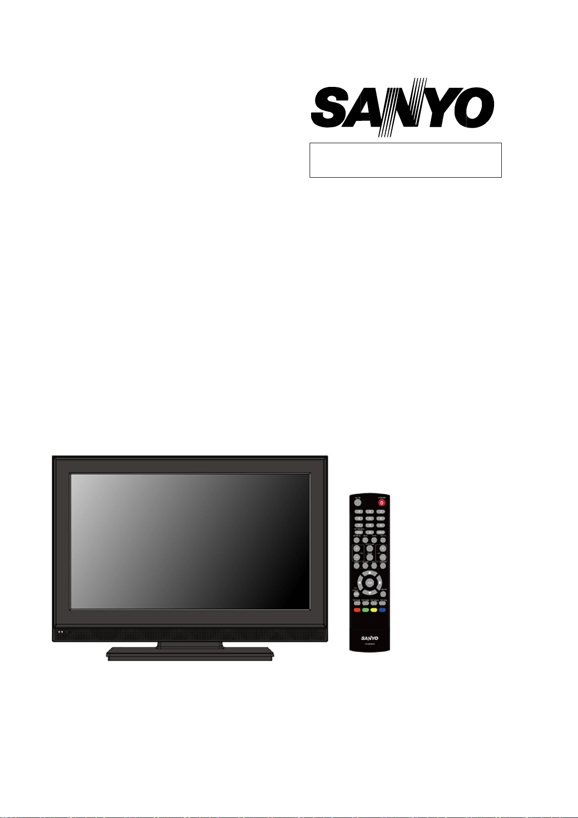
LCD TV
LCD-40E40F
PRODUCT CODE No.: 168234974 (3P AC Plug)
: 168234975 (2P AC Plug)
CHASSIS No.::::SSB40SM-00
CHASSIS No.::::SSB40SM-01
CHASSIS No.::::SSB40SA-00
CHASSIS No.::::SSB40SA-01
1
REFERENCE No.:
SM0945004-02
Page 2

CONTENTS
1. Safety precautions .................................................................................................
2. Alignment instructions and method of software upgrading.....................................
3. Working principle analysis of the unit ...................................................................
4. Block diagram ......................................................................................................
5. IC block diagram..................................................................................................
6. Wiring diagram ...................................................................................................
7. Troubleshooting guide..........................................................................................
8. Schematic diagram ..............................................................................................35
APPENDIX-A: Assembly list
APPENDIX-B: Exploded View
Removing or Installing the Stand
Wall mounting instructions
1
5
19
20
22
28
31
2
Page 3

Attention:
please read the following points carefully.
Safety precautions
This service manual is only for service personnel to take reference with. Before
servicing
1. Instructions
Be sure to switch off
inserting/plugging in connection wire Anti static measures to be taken (throughout the entire production
process!):
a) Do not touch here and there by hand at will;
b) Be sure to use anti static electric iron;
c) It’s a must for the welder to wear anti static gloves.
Please refer to the detailed list before replacing components that have special safety requirements.
Do not change the specs and type at will.
the power supply before
replacing or welding any components or
2. Points for attention in servicing of LCD
2.1 Screens are different from one model to another and therefore not interchangeable. Be sure to
Use the screen of the original model for replacement.
2.2 The operation voltage of LCD screen is
protecting yourself and the machine when testing the system in the course of normal operation or
right after the power is switched off. Please do not touch the circuit or the metal part of the module
high voltage. Be
sure to take proper measures in
That is in operation mode. Relevant operation is possible only one minute after the power is switched
off.
2.3 Do not use any adapter that is not identical with the TV set. Otherwise it will cause fire or damage
to the set.
2.4 Never operate the set or do any installation work in bad environment such as wet bathroom,
laundry, kitchen, or nearby fire source, heating equipment and devices or exposure to sunlight etc.
Otherwise bad effect will result.
2.5 If any foreign substance such as water, liquid, metal slices or other matters happens to fall into the
module, be sure to cut the power off immediately and do not move anything on the module lest it should
cause fire or electric shock due to contact with the high voltage or short circuit.
2.6 Should there be smoke, abnormal smell or sound from the module, please shut the power off at
once. Likewise, if the screen is not working after the power is on or in the course of operation, the
power must be cut off immediately and no more operation is allowed under the same condition.
2.7 Do not pull out or plug in the connection wire when the module is in operation or just after the
power is off because in this case relatively high voltage still remains in the capacitor of the driving
circuit. Please wait at least one minute before the pulling out or plugging in the connection wire.
2.8 When operating or installing LCD please don’t subject the LCD components to bending, twisting or
extrusion, collision lest mishap should result.
2.9 As most of the circuitry in LCD TV set is composed of CMOS integrated circuits, it’s necessary to
pay attention to anti statics. Before servicing LCD TV make sure to take anti static measure and
ensure full grounding for all the parts that have to be grounded.
2.10 There are lots of connection wires between parts behind the LCD screen. When servicing or
moving the set please take care not to touch or scratch them. Once they are damaged the screen
would be unable to work and no way to get it repaired.
If the connection wires, connections or components fixed by the thermo tropic glue need to disengage
when service, please soak the thermo tropic glue into the alcohol and then pull them out in case of
damage.
3
Page 4
2.11 Special care must be taken in transporting or handling it. Exquisite shock vibration may lead to
breakage of screen glass or damage to driving circuit. Therefore it must be packed in a strong case
before the transportation or handling.
2.12 For the storage make sure to put it in a place where the environment can be controlled so as to
prevent the temperature and humidity from exceeding the limits as specified in the manual. For
prolonged storage, it is necessary to house it in an anti-moisture bag and put them altogether in one
place.
The ambient conditions are tabulated as follows:
Temperature
Scope for operation
5
~+ 35
oC
Humidity
2.13
Display of a fixed picture for a long time may result in appearance of picture residue on the
screen, as commonly called “ghost shadow”. The extent of the residual picture varies with the maker
of LCD screen. This phenomenon doesn’t represent failure. This “ghost shadow” may remain
in the picture for a period of time (several minutes). But when operating it please avoid displaying still
picture in high brightness for a long time.
Scope for storage
Scope for operation
Scope for storage
0 ~
+ 40oC
0% ~
90
0% ~ 90%
%
3. Points for attention during installation
3.1 The front panel of LCD screen is of glass. When installing it please make sure to put it in place.
3.2 For service or installation it’s necessary to use specified screw lest it should damage the screen.
3.3 Be sure to take anti dust measures. Any foreign substance that happens to fall down between the
screen and the glass will affect the receiving and viewing effect
3.4 When dismantling or mounting the protective partition plate that is used for anti vibration and
insulation please take care to keep it in intactness so as to avoid hidden trouble.
3.5 Be sure to protect the cabinet from damage or scratch during service, dismantling or mounting.
4
Page 5
Alignment instructions
1. Test equipment
VG-848 (YPbPr, VGA signal generator)
VG-849 (HDMI signal generator)
FLUKE 54200(TV signal generator)
CA210
2. Power test
(white balancer)
Connect main board, power board and IR board according the wiring diagram, connect
the power and press power key (Remote controller or Keypad) button to turn on the TV.
a) Test the pin voltage of P802/power board , the data is shown in table1:
Table1 voltage data of P802
P802 Pin1,2
Voltage
Pin3,4 Pin5,6,7
GND 22.8-25.2V
For 40”
Pin8,9 Pin10,11,12
GND 11.4-12.6V 4.75-5.25V
On:2V-5.5V
Off: 0-0.5V
b) Test the pin voltage of P803/power board, the data is shown in table2:
Table2 voltage data of P803
P803 Pin1,2,3,4,5 Pin6,7,8,9,10
Voltage
22.8-25.2V GND NC 2.5V-5V 2.5-5V PWM NC
For 40”
Pin11 Pin12 Pin13 Pin14
Pin13 Pin14
<0.6V 2.5-5V PWM 2-5V
Pin15 Pin16
5
Page 6
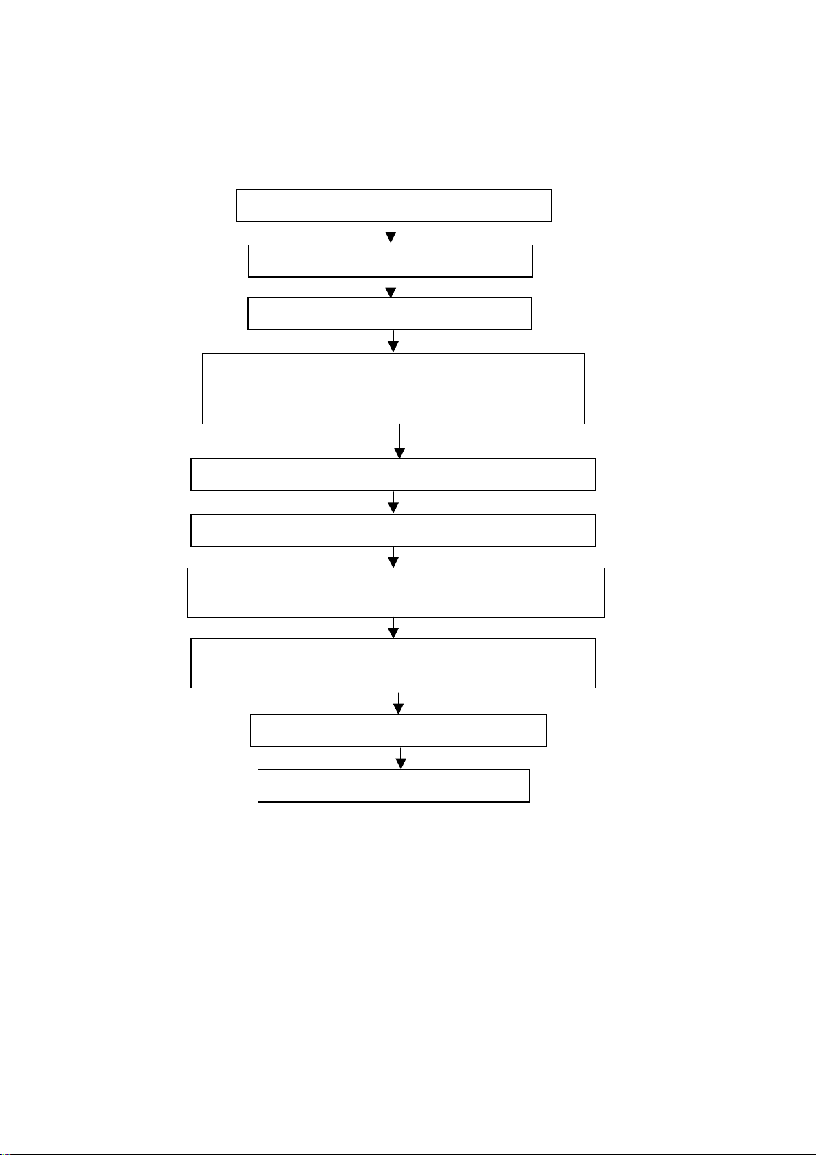
3. Alignment flow-chart
The alignment flow-chart is shown as fig-1
Connect to the center signal source and check each
Function of TV (station leaking, analog control, etc.)
Check the output of earphone and speaker.
Check if DDC, HDCP KEY, FLASH are written
Combined test for general assembly
White balance adjustment
Input AV/SVIDEO signal and check the function
Input HD signal and check the function of YPbPr
Input VGA signal and check if the display is normal, check
the function (analog control), horizontal/vertical center, etc.
Input HDMI signal and check if the display is normal, check
the function (analog control), horizontal/vertical center, etc.
Preset ex-factory
Check the accessories and packing
Fig-1 adjustment flow-chart
6
Page 7
4. Adjustment instruction
At any input source then press the “Mute” and “ Menu (key pad) to enter factory mode
During Factory menu, if “MENU” key is pushed, system will exit factory mode.
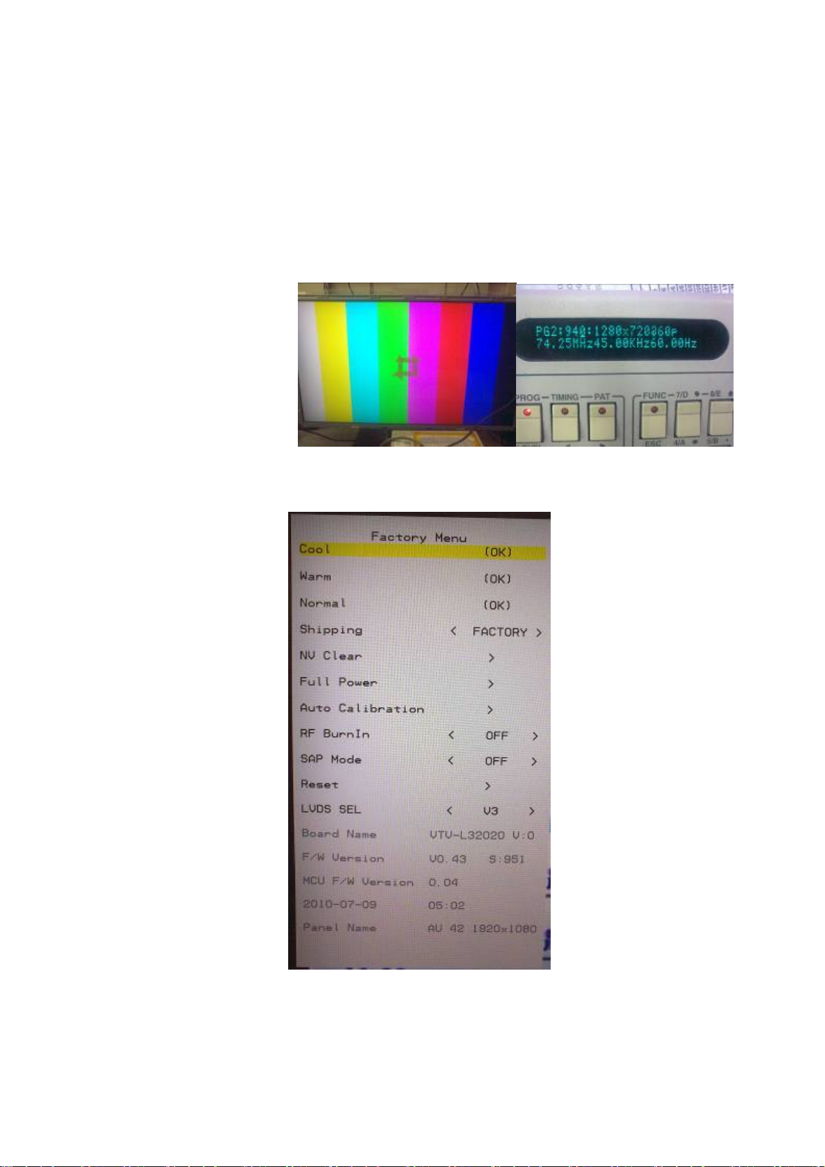
4-1. Source Calibration
4-1.1. Set the signal generator to input sources Video3 (Component) on LCD-TV; ASTRO-859 signal setting
to720P/60
(PG2 mode Timing 940 and Pattern 924 100% Color Bar.)
4-1.2. Entering into factory Mode: Press up or down key of remote control to select “Auto Calibration”, Press
「RIGHT」 key to enter the item.
-> Source calibration performed automatically when finished that will show OK.
7
Page 8
Repeat step 2 to do VGA input sources,
ASTRO-859 signal setting to1024X768 60Hz. (PG2 mode: Timing 963 and Pattern 924 100% color bar.)
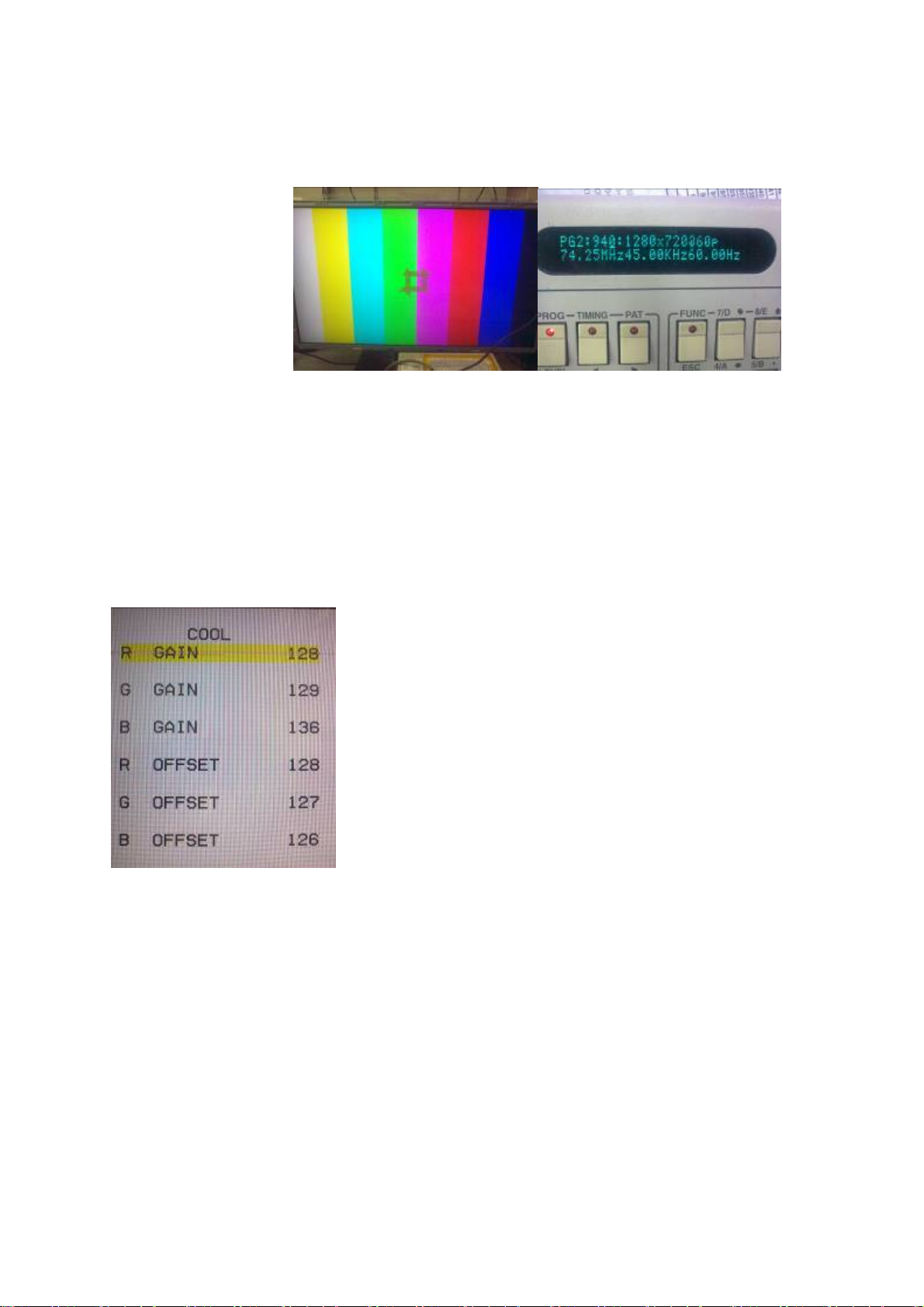
4-2. Color Temperature Adjustment & Check
4-2.1. Set the signal generator to RGB, 1024*768, 60HZ(ASTRO-859: PG1 856), Level:0.56V(80%). Full
white pattern.
4-2.2. Press up or down key of remote control to select “Cool”, Press 「ENTER」 key to enter the item.
RGAIN, GGAIN, BGAIN, ROFFSET, GOFFSET, BOFFSET, drive values are set for COOL, NORMAL, and
WARM independently.
4-2.3. Select 「Cool 」
Step 1.First Turning Gain parts of RGB.
(1) Cool spec.:
x= 0.267±0.030
y= 0.271±0.030
(2) If the x and y value are larger than specification,
Decrease R GAIN drive from default value.
Increase B GAIN drive from default value.
(3) If the x or y or both x and y value is/are smaller than specification.
Decrease B GAIN drive from default value
(4) According to a x and y value, please following adjustment of (4)-1 or (4)-2.
(4)-1 If x value is higher than spec
Decrease R GAIN drive from default value.
8
Page 9

Increase B GAIN drive from default value.
(4)-2 If y value is higher than spec,
Decrease B GAIN drive from default value
Step 2.When finsh Gain parts, then turning OFFSET parts
Set the signal generator to RGB, 1024*768, 60HZ(ASTRO-859: PG2 963), Level:0.217V(31%).
Full white pattern.
(1) Cool spec.: (Same as the Gain session )
x= 0.267±0.030
y= 0.271±0.030
(2) If the x and y value are larger than specification,
Decrease R OFFSET drive from default value.
Increase B OFFSET drive from default value.
(3) If the x or y or both x and y value is/are smaller than specification.
Decrease B OFFSET drive from default value
(4) According to a x and y value, please following adjustment of (4)-1 or (4)-2.
(4)-1 If x value is higher than spec
Decrease R OFFSET drive from default value.
Increase B OFFSET drive from default value.
(4)-2 If y value is higher than spec,
Decrease B OFFSET drive from default value
Step 3.When finsh OFFSET parts, then recheck Gain parts .unitl Both of them meet the
target specification
4-2.4. Select [NORMAL]
NORMAL spec.:
x=0.281±0.030
y=0.288±0.030
Adjust R drive (RED) or B drive (BLUE) to set x and y above.
4-2.5. Select [WARM]
WARM spec.:
x=0.301±0.030
y=0.31±0.030
Adjust R drive (RED) or B drive (BLUE) to set x and y above.
4-2.6. Exit Factory Mode:
After finish adjusting color temperature,press [MENU] to exit factory mode.
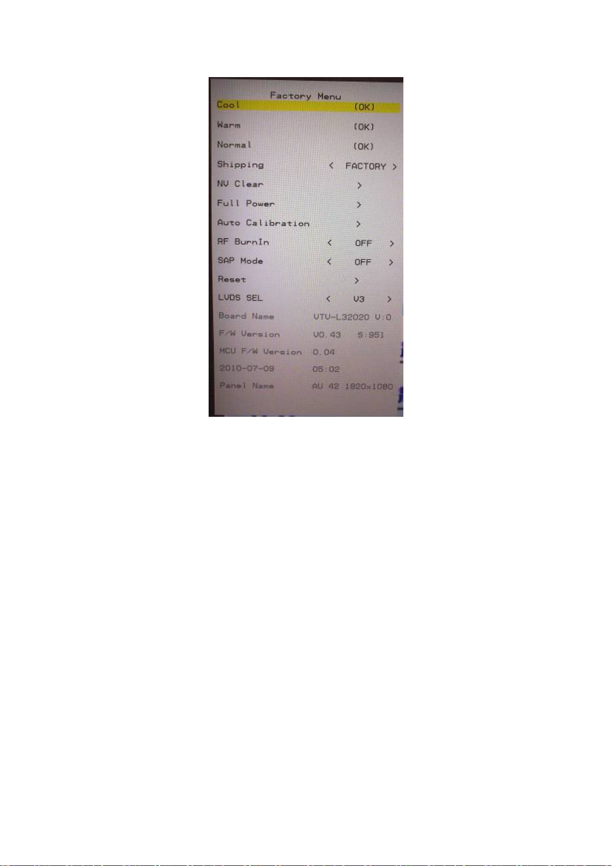
5. Items of Factory menu
Vendor may customize design and add adjustment items Factory menu as far as all required items are
included.
Press up and down key can move high light item from Cool ->Warm -> Normal ->Shipping-> NV clear-> Full
Power -> Auto Calibration -> RF Burn In -> SAP mode->Reset.
The NVRAM Clear and Reset to Default items will have a check dialog “yes or no” to do or not.
Push “OK” key can select high light item function. (Press right key can adjust value)
Display Board name, firmware version, Panel name and released date on bottom.
9
Page 10
5-1) Cool
Press up or down key can select high light item function.
Press OK key to enter the item.
Following data for color temp shall be edited manually.
-R, G, B data for each preset.
-Press “Up” or “Down” key to select “R”, “G”, “B” Gain and Offset item
-Press “Left” or “Right” key to set the “R”, “G”, “B” Gain and Offset value.
- Press “MENU” or “BACK” item to exit to factory mode
5-2) Warm
Press up or down key can select high light item function.
Press OK key to enter the item.
Following data for color temp shall be edited manually.
-R, G, B data for each preset.
-Press “Up” or “Down” key to select “R”, “G”, “B” Gain and Offset item
-Press “Left” or “Right” key to set the “R”, “G”, “B” Gain and Offset value.
- Press “MENU” or “BACK” item to exit to factory mode
5-3) Normal
Press up or down key can select high light item function.
Press OK key to enter the item.
Following data for color temp shall be edited manually.
-R, G, B data for each preset.
-Press “Up” or “Down” key to select “R”, “G”, “B” Gain and Offset item
-Press “Left” or “Right” key to set the “R”, “G”, “B” Gain and Offset value.
10
Page 11

-Press “MENU” or “BACK” item to exit to factory mode
5-4)Shipping
Press up or down key can select high light item function
Press “Left” & “Right” key to select the item. Default set in Factory mode
Following shipping area to select the item(ME)
5-5) NVRAM Clear
Initialize program’s default values to NVRAM for following adjustment items accuracy.
In factory mode it is the first and important step to make sure all values are default value and correct.
- Reset settings: Gamma table, Channel table (Favorite channel, Channel label etc.), Model table
(H/V Position, Clock, Phase), Source dependent setting (Contrast, Brightness etc.), Common
setting (Volume, Language etc.), Parental Control (Rating, Password etc).
To avoid a mistake initial process after factory setting is done. This item will have a check dialog “yes or no”
to do the initial or not.
NOTICE:
This item just enabled in PC input and after this item is processed then the DUT needs to be powered off
then AC powered off.
5-6) Full power
This is for power consumption testing.
To measure the maximum power consumption of TV set, we adjust the value of following items to maximum.
- Contrast
- Brightness
- Audio output
5-7) Auto Calibration
Auto Calibration (gain/offset) must be adjusted color by firmware automatic adjustment in PC and
Video3(Component) input source.
5-8) RF Burn In
Use “snow” pattern for burn in. Selected items are “On” and “Off”.
While turn on burn in mode, firmware will automatically turn off “Auto power off” function.
If there is no power supply suddenly, firmware will re-enter burn in mode automatically when power supply is back.
Selected RF Burn In items to Off or Reset Items to reset TV , firmware will turn off burn in mode
Burn in mode: Source is “ANT”, Input Configuration is “Antenna” and channel is NTSC channel 2.
5-9) SAP Mode.
N/A
5-10) Reset
Reset all settings of OSD menu to default value and will go to standby mode.
- Reset settings: Channel table, Model table (H/V Position, Clock, Phase), Source dependent setting
(Contrast, Brightness etc.), Common setting (Volume, Language etc.)
11
Page 12
6. Dealer Mode Function
7. Performance check
7-1 TV function
Connect RF to the center signal source, enter Channel menu → auto tuning, check if there are channels be
skipped, check if the picture and speaker are normal.
7-2 AV/S-Video terminals
Input AV/S-Video signal, check if the picture and sound are normal.
7-3 YPbPr/YCbCr terminal
Input YUV signal (VG848 signal generator), separately input the YUV signals listed in table4 and check if the
display and sound are normal at any situation (power on, channel switch and format convert, etc.)
7-4 VGA terminal
Input VGA signal (VG848 signal generator), separately input the signals listed in table5 and check the display and
sound. If the image is deflection of the Horizontal and vertical, select Menu->Setup->Auto Adjust to perform autocorrect.
Table4 YUV signal format
Table5 VGA signal format
12
Page 13
7-5 HDMI terminal
Input HDMI signal (VG849 signal generator), separately input the signals listed in table4 and table5 and check the
display and sound (32 KHz, 44.1 KHz, 48 KHz) at any situation (power on, channel switch and format convert,
etc.)
7-6 other functions check
a) Check the turn on/turn off timer, sleep timer, picture/sound mode, OSD, stereo and analog TV Teletext, etc.
8. Software instruction
Update S/W tool
Tools setting.
Connector to PC and VTV_T42006 use USB cable
Connect VTV_L32020 and VTV_T42006 use special VGA cable.
13
Page 14
Don’t push blue Key.
SoftWare seeting.
1. press Option to check ISP mode, Packet size and Default baud rate then press OK
2. select communication COM port.
14
Page 15
15
Page 16
3. press Select File then select update F/W file.
4. press Start
16
Page 17
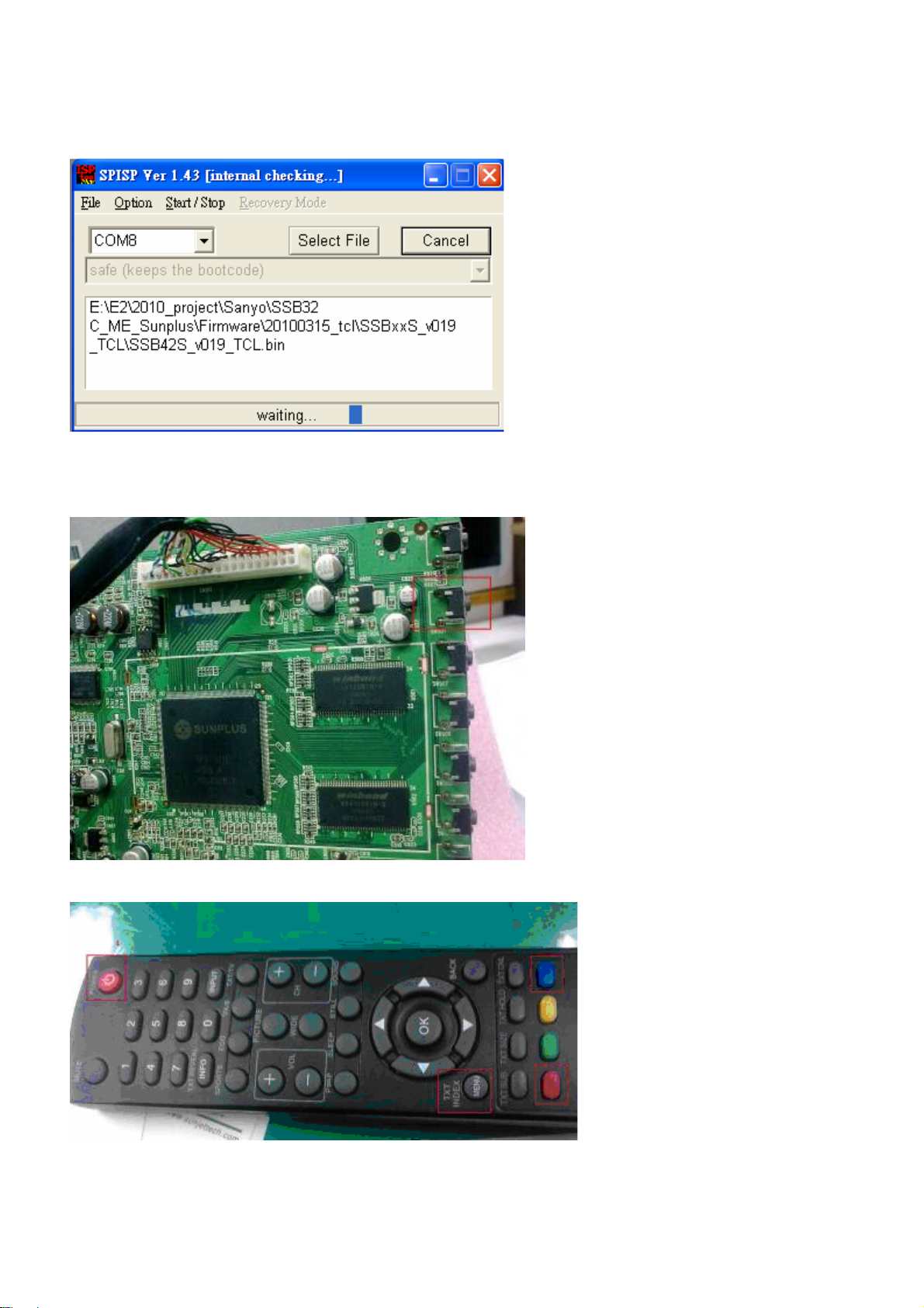
5.start update F/W, there has two method to start update F/W
(1)keep push Channel up key and turn on the power.
(2)press Menu key then red key then blue key then Power key to update F/W.
17
Page 18

6.Erasing EE PROM
7.Build in F/W on the EE PROM.
8. update success.
18
Page 19

Working principle analysis of the unit
1. PAL/SECAM
Antenna reception, B/G, I, D/K, signal will be send to tuner M40CPT-2PNB-E,
demodulating and output standard video signal TV-CVBS, and sound SIF signal
and NTSC
signals flow:
t he n T u n er w i l l b e
.
TV-CVBS will send to the master control IC SPV7101P to video decode, de-interlace and scaler, then
output
LVDS level drive for panel display.
The
sound IF (SIF) will be fed into SPV7101P, after demodulating, pre-amplifying, bass adjusting
and volume control, the sound signal will
tr a n sf o rm into d ig i ta l I2S s ig n al
speaker, another will be sent analog sound signal to
2. Composite/S-Video signal flow
Composite signal and S-Video signal path AV signal switch
be ou t p ut t wo w a y s , o n e w a y w i ll b e
and sent to digital amplifier STA335BW,
earphone amplifier TPA6132.
then sent to
by menu “Setup”->“Video1 Input”
via
terminal socket to Video switch IC NC7SB3157, then signal and the Video2 path AV signal will be
fed to SPV7101P to perform video decode, de-interlace and scaler, then output LVDS drive level for
panel display.
Audio signal from Composite/S-Video
adjust and volume control, the sound signal will
tr a n sf o rm in t o d i gi t al I 2 S si g na l
speaker, another will be sent analog sound signal to
3. PC/Video3 signal flow
PC and the Video3 path
via terminal
to back end module to Video decode,
drive
for panel display.
Sound signal of PC/YPrPb
adjust
and volume control, the sound signal will
tr a n sf o rm in t o d i gi t al I 2 S si g na l
speaker, another will be sent analog sound signal to
4. HDMI signal flow
socket
terminal
via matched resistance is fed to SPV7101P to bass
b e o u t p u t t w o w a y s , o n e w a y w il l b e
and sent to digital amplifier STA335BW,
earphone amplifier TPA6132.
Composite/
YPbPr signal
switch by menu”SET UP”->”Video3 Input”
sent to SPV7101P A/D conversion(YPbPr),
de- interlace and
image scale, then send to LVDS level
t e r m i n a l
via matched resistance
b e o u t p u t t w o w a y s , o n e w a y w il l b e
and sent to digital amplifier STA335BW,
earphone amplifier TPA6132.
PC/YP b Pr
a n d
sent to SPV7101P to bass
then sent to
output R/G/B of 24 bit
then sent to
Three HDMI video signals via switcher IT6633P are directly fed to the master control IC SPV7101P to
digital
decode, image scale, then output LVDS drive level for panel display. HDMI audio signal via
decoder built-in SPV7101P to bass adjust and volume control, the sound signal will
wa y s , o ne wa y w i l l b e t r an s f o r m i n to di g it a l I 2 S s ig n a l
STA335BW,
TPA6132.
then sent to speaker, another will be sent analog sound signal to
and sent to digital amplifier
b e o u tp u t t w o
earphone amplifier
19
Page 20

I. Block Diagram
Sanyo 40” Block Diagram
20
Page 21

Block diagram-POWER-40”
21
Page 22

IC block diagram
1.SUNPLUS SPV7101P
Feature:
Graphics and Video Input Port
Integrate 150MHz 10-bit ADC/PLL
Dual CCIR656 digital video ports to support 2 input or 1 input/1output
Support SDTV at 480i/576i and 480p 576p
Support HDTV at 720p,1080i and 1080p
Support PC graphics VGA, SVGA, XGA, WXGA, SXGA@75Hz(135M)
Built-in sync. Processor for separate, composite or sync onY/G
Image Format Detection/Auto Image Positioning/Auto Phase Detection
Full SCART support including RGB fast blank
HDMI
HDMI1.2 compliant and DVI 1.0 compliant receiver
HDCP 1.1 compliant receiver
HDMI 1.3 CEC protocol compliant
Support 480i/576i/480p576p/720p/1080i/1080p resolutions
S/PDIF output supports PCM, Dolby Digital, DTS digital audio with bypass
mode
Four I2S audio outputs to SSD(Stereo Sound Decoder) with bypass mode
Auto audio error detection with programmable soft mute
Built-in OTP for HDCP key
3D Video Decoder
Enhanced NTSC/PAL/SECAM video decoder
3D comb filter for NTSC, PAL I(B,G,H,D,N), PAL-M, PAL-N
Enhanced NTSC/PAL/SECAM auto detection
4 analog input and one analog video output
Enhanced Cross-color reduction for NTSC by 3-line comb filtering
Enhanced Cross-color reduction for PAL by 5-line comb filtering
Enhanced Motion adaptive 3D Y/C separation comb filter for NTSC/PAL system
Enhanced Multi-standard VBI data decoder, Teletext 2.5, WSS,VPS,
Closed-caption and V-chip
Macrovision detection
VBI data(C.CTTX2.5, V-chip)overlay display
High Quality Video Processing
Enhanced pixel-based SDTV/HDTV 3D motion adaptive de-interlacing
Enhanced 2:2/3:2 film mode detection
Support Graphics mode frame rate conversion
Support Video mode frame rate conversion
2D Edge enhancement
Enhanced Dynamic Peaking Filter
Enhanced Digital Luma Transient Improvement(DLTI)
Enhanced Digital Chroma Transient Improvement(DCTI)
Black/White Level Expansion and Dynamic Contrast
Enhanced RGBYMC color adjustment
Dark and Gray area UV suppression
Enhanced 3D motion adaptive noise reduction
De-blocking and de-mosquito filters
Enhanced color management/color temperature adjustment
Brightness/Contrast/Hue/Saturation adjustment
Support RGB color correction
Built-in three 256-point gamma tables with 10 bits resolution
Color space conversion, both YCbCr to RGB and RGB toYCbCr
Built-in temporal/spatial color dithering
10-bit video/image processing
22
Page 23

High Quality Video Scaling Engine
Advanced fourth-generation scaling engine
Support 4:3 /16:9 with non-linear scaling
Support moiré Canceling
Multi-standard TV Sound Decoder
Fidel proven TV sound decoder
Support BTSC, A2/Zweiton, NICAM, EIAJ, SECAM, and FM stereo
Automatic TV-standard detection(ADS)
Non-standard carrier compatible
SAP decoding where applicable
Auto fallback from NICAM where applicable
Embedded OSD and VBI controller
Built-in programmable OSD engine for two OSD windows(bitmap OSD)
1,2,4 and 8-bit per pixel(bitmap OSD)
Support hardware cursor
Support programmable 512 font-based OSD and Graphics-based OSD
Support VBI decoder(CC, V-Chip and Teletext)
Support VBI CC/TTX/Menu with more than 1000 char-fonts
Embedded SDR/DDR SDRM Controller
Integrated SDR/DDR SDRAM controller with DLL(DDR)
Support 32-bit DRAM bus with memory size from 16Mb(limited functions) to
256Mb
Programmable Digital Output for LCD
Support output sequence mapping for TI and Thine
Built-in dual-channel 8-bit LVDS Transmitter or single channel 10-bit LVDS
Transmitter
Support display output up to 1920X1200 @60Hz WUXGA reduced blanking
mode(Supported by SPV7101Px only)
Support Power Down Sequence
4-channel PWM backlight intensity control
Note Dolby Surround is the Trade Mark of Dolby Laboratories SRS TurSurround is
the Trademark of SRS
CPU
Powerful 32-bit RISC CPU
Simple memory management stub(SMMU)
MIPS-I instruction with DSP instruction set extension
2K byte 2-way instruction cache
4K bytes direct-mapped data cache
8K byes data memory for DMA operation
EJTAG interface
One UART up to 115200 baud rate
Four 24-bit up/down timers
3K byes IMEM for power saving mode.
Audio Processor
Support S/PDIF input
Support S/PDIF output(signal could come from S/PDIF input or SSD)
Support up to 8 channels I2S I/O
4channels audio DAC output
4channels audio ADC input
Channel: L,R,C,S,Sub, Aux1,2 and 3 @ 32KHz
5-band equalizer
3D surround sound
Bass management
Volume control
Support sub-woofer output
Sample rate converter
23
Page 24

SSD could output up to 3 sources
Dolby Surround (VDSII 422 and 423)(Supported by SPV7101PD only)
SRS TruSurround(XT, WOW,3D sound)(Supported by SPV7101PS only)
Miscellaneous
Built-in TV remote control via infra-red receiver interface
2-channel 6-bit ADC for key scan function
Built-in pattern generator for auto testing
256-pin LQFP(SPV7100P pin-to-pin compatible)
2. M40CTP-2PNB-E
Analog terrestrial video module
3. STA335BW
20-W Stereo Digital Audio Power Amplifier with EQ and DRC
24
Page 25

4. IT6633E-P
3-to-1 HDMI 1.3 Active Switch with EDID RAM
25
Page 26

5. TPA6132A2
25-mW DIRECTPATH STEREO HEADPHONE AMPLIFIER WITH POP
SUPPRESSION
26
Page 27

6. WT6702F
The WT6702F is a microcontroller for system power manager with 1)Turbo 8051
compatible(3T) CPU2) 8K bytes flash memory, 3)256 bytes SRAM, 4) 2
PWMs,5)DPMS detector, 6)8051 2 timers and UART,7)Three Slave IIC interface,
8) 4 Channel 8-bit A/D converter, 9) Real Time Clock, 10) watch-dog timer, 11)
Embedded ISP, 12)Power down mode, 12) Embedded ICE mode.
27
Page 28

I. BLOCK
Sanyo 40-inch Wiring Diagram
28
Page 29

II. Wiring Connection
CMO panel
29
Page 30

Samsung panel
30
Page 31

Trouble shooting
1. Fault clearance
31
Page 32

Change to new power board.
Check
Check L21
OK
NG
H
L
Power LED no
Change MAIN
Change LED
NG
2. Troubleshooting guide
The flow chart shown below will help you to troubleshoot your Televison set with it doesn’t display
normally. Each procedure offers a simple way to check for system errors. Before starting, ensure
that there is a signal in and that the Televison is turned on.
2-1 Power LED no light
Light
+5V_IN
CN2
Pin 2
Check
LED
P/N:
PK101V1110I or PK101V2070I
PCB
PCB
32
Page 33

Change to new power board.
2-2 Has audio but no video out
P/N: PK101V1110I or
PK101V2070I
33
Page 34

Change to new power board.
2-3 Has video but no audio out step 1
2-4 Has video but no audio out step 2
P/N:
PK101V1110I or
PK101V2070I
34
Page 35

8.SCHEMATIC DIAGRAM
ELECTRON (LCD-40E40F)
Page 36

5
C823
C823
82pF
C803
C803
R801 10KR801 10K
C811
C811
22pF/50V
22pF/50V
82pF
1uF/50V/0805
1uF/50V/0805
3.3nF/50V
3.3nF/50V
R804
R804
6.2K/1%
6.2K/1%
APW7085
APW7085
C809
C809
D D
C C
scaler
1.8V digital- 0.75A
1.8V analog - 0.34A
3.3V digital- 45mA MAX
3.3V analog- 55mA MAX
100k ----> 10k
SPV7100 Power (1.8V/2.5V/3.3V)
4
L802
L802
BLM21PG300SN1D
C802
C802
SE22uF/16V
SE22uF/16V
U801
U801
4
2
6
BLM21PG300SN1D
1
VIN
VCC
EN
COMP
below current measure timming
1080P 60
full white pattern
UGND
LX
FB
GND
8
THERMAL
9
3
5
7
+5V_SW
C804
C804
1uF/50V/0805
1uF/50V/0805
R806
R806
10K/1%
10K/1%
3
Vout=0.8(1+R1/R2)
C808 D801close U801
L804
L804
SMTDR43-3.3uH/1.44A
SMTDR43-3.3uH/1.44A
D801
D801
SM540B
SM540B
1 2
1 2
R805
R805
13K/1%
13K/1%
C812
C812
270pF/50V
270pF/50V
Del C813 1/13
HDMI 690mA
PC 620mA
L801
L801
BLM21PG300SN1D
BLM21PG300SN1D
+
+
C808
C808
SE100uF/16V
SE100uF/16V
1.85V~1.88V
+1V8
VCC3_3
C844
C844
82pF
82pF
2
U802
U802
LD1117AL-ADJ-223-1 A
LD1117AL-ADJ-223-1 A
3
VIN
1
C807
C807
0.1uF
0.1uF
C0603D
C0603D
C810
C810
SE10uF/16V
SE10uF/16V
ADJ
VOUT
TAB
2
4
R802
R802
121/1%/
121/1%/
R803
R803
54.9/1%
54.9/1%
C805
C805
0.1uF
0.1uF
C0603D
C0603D
G_PWR
C806
C806
SE100uF/16V
SE100uF/16V
L803
L803
L1206D
L1206D
1
HDMI 1.mA
Analog 74.2 mA
pc 163mA
+1V8_ADCA
+5V_SW
U803 UTC1084-3.3V-252U803 UTC1084-3.3V-252
GND
OUT
TAB
1
2
4
R807
R807
910/1%/
910/1%/
R808
R808
1K/1%
1K/1%
2
C820
C820
SE100uF/16V
SE100uF/16V
G_PWR
DDR
C826
C826
0.1uF
0.1uF
C0603D
C0603D
G_PWR
C816
C816
100nF
100nF
HDMI 160mA
KC PBMA-L11-321611-300LMA60T
KC PBMA-L11-321611-300LMA60T
C827
C827
SE100uF/16V
SE100uF/16V
VIN3VOUT
C818
C818
SE100uF/16V/NC
SE100uF/16V/NC
B B
+5V_SW
A A
del C825 7/27
C821
C821
82pF
82pF
C822
C822
82pF
82pF
SE10uF/16V
SE10uF/16V
C819
C819
100nF
100nF
U806
U806
LD1117AL-ADJ-223-1 A
LD1117AL-ADJ-223-1 A
3
VIN
GND
1
C828
C828
0.1uF
0.1uF
C0603D
C0603D
C829
C829
Ypbpr/PC 340mA AV 90mA
L807
L807
KC PBMA-L11-321611-300LMA60T
KC PBMA-L11-321611-300LMA60T
KC PBMA-L11-321611-300LMA60T
KC PBMA-L11-321611-300LMA60T
KC PBMA-L11-321611-300LMA60T
KC PBMA-L11-321611-300LMA60T
KC PBMA-L11-321611-300LMA60T
KC PBMA-L11-321611-300LMA60T
All source 190mA
L812
L812
71mA
L808
L808
L809
L809
L810
L810
HDMI/other 170mA ATV 220mA
切切
other source 仍仍160mA, 不仍HDMI source
+2V5
VCC3_3
+3V3
+3.3V_HD
+3V3_STBC
應應應應
10mA
C824
C824
82pF
82pF
MCU
+5V_S
Power & Ground 4
5
4
3
U804
U804
LD1117-3.3V-223-1A
LD1117-3.3V-223-1A
3
VIN
C814
C814
100nF
100nF
TP801TP801
2
OUT
4
TAB
GND
1
C815
C815
100nF
100nF
2
C817
C817
SE100uF/16V
SE100uF/16V
G_PWR
L806
L806
KC PBMA-L11-321611-300LMA60T
KC PBMA-L11-321611-300LMA60T
Title
Title
Title
Size Docum ent Number Rev
Size Docum ent Number Rev
Size Docum ent Number Rev
B
B
B
Date: Sheet of
Date: Sheet of
Date: Sheet of
3V3_MCU
COMPAL OPTOELECTRONICS CO., LTD
COMPAL OPTOELECTRONICS CO., LTD
COMPAL OPTOELECTRONICS CO., LTD
SCHEMATIC, M/B VTV-L32020, SSB32S
SCHEMATIC, M/B VTV-L32020, SSB32S
SCHEMATIC, M/B VTV-L32020, SSB32S
401C2M
401C2M
401C2M
2 15Tuesday, July 27, 2010
2 15Tuesday, July 27, 2010
2 15Tuesday, July 27, 2010
1
0A
0A
0A
Page 37

5
D D
4
3
2
1
R306
R306
RX
TX
B_IN
R_IN
SOG_IN
B_IN <6>
G_IN <6>
R_IN <6>
SOG_IN <6>
R307
R307
R308
R308
R302 100R /0402R302 100R /0402
R303 100R /0402R303 100R /0402
R304 100R /0402R304 100R /0402
R305 100R /0402R305 100R /0402
C302 0.01uF /0402/50VC302 0.01uF /0402/50V
C303 0.01uF /0402/50VC303 0.01uF /0402/50V
C304 0.01uF /0402/50VC304 0.01uF /0402/50V
C301 1nF/04 02/50VC301 1nF/04 02/50V
Close to SCALER IC
R361
D314
D314
R361
R362
R362
D315
D315
D302
D302
0R/0402
0R/0402
0R/0402
0R/0402
D303
D303
D-SUB INPUT
C C
VSI
HSI
DSUB-15P/FEMALE/V
DSUB-15P/FEMALE/V
JP301
JP301
15
14
13
12
11
5
10
4
9
3
8
2
7
1
1611
1611
6
16 17
+5V_PC
VGA_B+
VGA_G+ G_IN
VGA_R+
TXD <6,8>
RXD <6 ,8>
D304
D304
D305
D305
These components close to SPV7100
75R/0402/1%
75R/0402/1%
75R/0402/1%
75R/0402/1%
QV1AA10P-R05/NC
QV1AA10P-R05/NC
QV1AA10P-R05/NC
QV1AA10P-R05/NC
QV1AA10P-R05/NC
QV1AA10P-R05/NC
HSI HS_VGA
B B
D301
C305
C305
D301
QV1AA10P-R05/NC
QV1AA10P-R05/NC
D308
D308
QV1AA10P-R05/NC
QV1AA10P-R05/NC
0.1uF/0402/16V
0.1uF/0402/16V
U301
U301
1
NC
2
NC
3
NC
GND4SDA
24C02/SOP8
24C02/SOP8
4
R315
R315
4.7K/0402
4.7K/0402
VCC
VCLK
SCL
8
7
6
5
D306
D306
QV1AA10P-R05/NC
QV1AA10P-R05/NC
D307
D307
QV1AA10P-R05/NC
QV1AA10P-R05/NC
A A
5
+5V_SW
TP301TP301
+5V_PC
1
2
D309 BAT54C/SOT -23D309 BAT 54C/SOT-23
3
QV1AA10P-R05/NC
QV1AA10P-R05/NC
R316
R316
4.7K/0402
4.7K/0402
R318
R318
10K/0402
10K/0402
QV1AA10P-R05/NC
QV1AA10P-R05/NC
R317
R317
100R/0402
100R/0402
PC_WP
QV1AA10P-R05/NC
QV1AA10P-R05/NC
100R/0402
100R/0402
R301
R301
75R/0402/1%
SCL_VGA
SDA_VGA
75R/0402/1%
PC_WP <6>
SCL_VGA <8>
SDA_VGA <8>
3
Change1
R309 1K/0402R309 1K/0402
R310 10K/0402R310 10K/0402
R311 1K/0402R311 1K/0402
R312 10K/0402R312 10K/0402
HS_VGA <6>
VS_VGAVSI
COMPAL OPTOELECTRONICS CO., LTD
COMPAL OPTOELECTRONICS CO., LTD
COMPAL OPTOELECTRONICS CO., LTD
Title
Title
Title
SCHEMATIC, M/B VTV-L32020, SSB32S
SCHEMATIC, M/B VTV-L32020, SSB32S
SCHEMATIC, M/B VTV-L32020, SSB32S
ize Docum ent Number Rev
Size Docum ent Number Rev
Size Docum ent Number Rev
S
B
B
B
Date: Sheet of
Date: Sheet of
2
Date: Sheet of
401C2M
401C2M
401C2M
VS_VGA <6>
1
0A
0A
0A
3 15Monday, September 20, 2010
3 15Monday, September 20, 2010
3 15Monday, September 20, 2010
Page 38

5
CVBS & Ypbpr AV input
JP302B
JP302B
D D
MKC21-029PV
MKC21-029PV
Ypbpr_G
T5
S5
SC1_AU_LOUT
CVBS_TU_OUT1
C327 2.2uFC327 2.2uF
C330 2.2uFC330 2.2uF
R347
R347
47K
47K
AOUT0L
AOUT0R
R348
R348
47K
47K
T6
S6
T7
S7
T8
B8
S8
Side AV input
R343
C C
270pF/25V/0402
JP304
JP304
FRON-AV-KYOYAKU
FRON-AV-KYOYAKU
R_S
R_S
3
2
R
GND
R
GND
1
L_S
L_S
6
5
L
GND
L
GND
4
V_S
V_S
9
8
CVBS
GND
CVBS
GND
7
Video Output
+5V_SW
L301
L301
FBMA-300LMT
FBMA-300LMT
C334
CVBSO
C334
10uF/0805/10V
10uF/0805/10V
GNDV
C336
C336
10uF/0805/10V
10uF/0805/10V
B B
CVBSO<6>
270pF/25V/0402
270pF/25V/0402
270pF/25V/0402
100pF/25V/0402/NC
100pF/25V/0402/NC
C335
C335
0.1uF
0.1uF C314
R351
R351
R352
R352
220R
220R
10K
10K
C
Q302
Q302
B
PMBT3904
PMBT3904
E
R357
R357
R356
R356
75R
75R
12K
12K
GNDV
R343
10K
10K
C328
C328
C331
C331
C333
C333
R3530RR353
0R
R344
R344
6.8K
6.8K
R345
R345
10K
10K
R346
R346
6.8K
6.8K
L312
L312
1.8uH
1.8uH
C348
C348
C347
C347
220pF
220pF
220pF
220pF
EC
Q301
Q301
B
PMBT3906
PMBT3906
R354
R354
75R
75R
C363 SE10uF/16VC363 SE10uF/16V
CVBS0_IN_A
C362 SE10uF/16VC362 SE10uF/16V
AOUT0L <6>
AOUT0R <6>
SC1_AU_ROUT
MMBT3904L
MMBT3904L
Add Q303 Q304 R364 R365 for Fix DC/ON Po noise 7/23
C329
C329
560pF/25V/0402
560pF/25V/0402
C332
C332
560pF/25V/0402
560pF/25V/0402
R35075R350
75
C364
C364
+
+
CVBS_TU_OUT1
220uF 6.3V
220uF 6.3V
VGA audio input
L307
2
1
L307
KHB0805Q300SA
KHB0805Q300SA
L308
L308
KHB0805Q300SA
KHB0805Q300SA
270pF/25V/0402
270pF/25V/0402
270pF/25V/0402
270pF/25V/0402
JP305
JP305
R
T
3
S
PhoneJack-SHI-BLU 3P
PhoneJack-SHI-BLU 3P
A A
PC Audio
Input
5
R355
R355
10K
10K
C337
C337
C339
C339
R358
R358
6.8K
6.8K
R359
R359
10K
10K
R360
R360
6.8K
6.8K
AIN3R
C338
C338
560pF/25V/0402
560pF/25V/0402
AIN3L
C340
C340
560pF/25V/0402
560pF/25V/0402
Y/CVBS SWITCH
R387
R387
4.7K/0402
4.7K/0402
R385
R385
4.7K/0402
4.7K/0402
+5V_SW
R364
R364
C
Q304
Q304
E
AIN1L
R349
R349
CVBS2_IN
100/1%/0402
100/1%/0402
AIN3R <6>
AIN3L <6>
4
+5V_SW
GND
SC1_AU_LOUT
MMBT3904L
MMBT3904L
4.7K
4.7K
AVout_Mute
AVout_Mute
B
AIN1R
JP306
JP306
1
EARPHONE/SW/KYOYAKU
EARPHONE/SW/KYOYAKU
4
SW_CON Output
0 CVBS1
1 S_Video
R388
R388
4.7K/0402
4.7K/0402
1
2
3
NC7SB3157P6X
GND
+5V_SW
R365
R365
4.7K
4.7K
C
B
E
AVout_Mute <6>
AIN1L <6>
AIN1R <6>
CVBS2_IN <6>
NC7SB3157P6X
Close SPV7101
AVout_Mute
JP303
JP303
JALCO / AV SV-IN_V
JALCO / AV SV-IN_V
R386
R386
4.7K/0402
4.7K/0402
Q303
Q303
EARPHONE
678
2L3R
4L5R
91011
B1
GND
B0
U302
U302
Vcc
5
CVBS
CVBS
Audio L
Audio L
Audio R
Audio R
6
S
5
4
A
6
S_SWS_GND
S_SWS_GND
TOP_C
TOP_C
TOP_Y
TOP_Y
GND
GND
GND
GND
GND
GND
+5V_SW
R3840R384
0
R331
R331
100/1%/0402
100/1%/0402
C345
C345
0.1uF/25V/0402
0.1uF/25V/0402
GND
JP302A
JP302A
MKC21-029PV
MKC21-029PV
T1
S1
T2
S2
T3
S3
T4
B4
S4
S-AV Input
4
3
GND
GND
2
GND
GND
1
YT
100pF/25V/0402/NC
YS
WT
WS
RT
RB
RS
D316
D316
QV1AA10P-R05/NC
QV1AA10P-R05/NC
100pF/25V/0402/NC
D317
D317
D318
D318
QV1AA10P-R05/NC
QV1AA10P-R05/NC
QV1AA10P-R05/NC
QV1AA10P-R05/NC
L314
L314
3
SW_CONSV_Y_IN
CVBS0_IN <6>
GND_IO
100pF/25V/0402/NC
100pF/25V/0402/NC
100pF/25V/0402/NC
100pF/25V/0402/NC
270pF/25V/0402
270pF/25V/0402
270pF/25V/0402
270pF/25V/0402
C350
C350
L313
L313
430pF/0603/50V/NC
430pF/0603/50V/NC
3.3uH/KSI0603
3.3uH/KSI0603
3.3uH/KSI0603
3.3uH/KSI0603
3
SW_CON <6>
C311
C311
C314
C344
C344
C358
C358
C343
C343
C352
C352
470pF/0603/50V
470pF/0603/50V
L317
L317
KHB0805Q300SA
KHB0805Q300SA
L0805D
C308
430pF/NC
430pF/NC
C312
C312
C316
C316
C323
C323
L309
L309
1.8uH
1.8uH
L310
L310
1.8uH
1.8uH
L316
L316
1.8uH
1.8uH
220pF
220pF
R368
R368
6.8K
6.8K
430pF/0603/50V/NC
430pF/0603/50V/NC
L315
L315
3.3uH/KSI0603
3.3uH/KSI0603
C342
C342
220pF
220pF
C359
C359
220pF
220pF
C355
C355
L0805D
KHB0805Q300SA
KHB0805Q300SA
KHB0805Q300SA
KHB0805Q300SA
R369
R369
6.8K
6.8K
C353
C353
KHB0805Q300SA
KHB0805Q300SA
KHB0805Q300SA
KHB0805Q300SA
KHB0805Q300SA
KHB0805Q300SA
AIN2R
Ypbpr_G HD1Y
430pF/NC
430pF/NC
430pF/NC
430pF/NC
C320
C320
270pF/25V/0402
270pF/25V/0402
270pF/25V/0402
270pF/25V/0402
C361
C361
220pF
220pF
C360
C360
220pF
220pF
C356
C356
220pF
220pF
R367
R367
10K
10K
R371
R371
10K
10K
C351
C351
L302
L302
L0805D
L0805D
L303
L303
L0805D
L0805D
L304
L304
L0805D
L0805D
L305
L305
L0805D
L0805D
L306
L306
L0805D
L0805D
R32275R322
75
R32875R328
75
0/1%/0402
0/1%/0402
R33675R336
75
AIN2L
C357
C357
560pF/25V/0402
560pF/25V/0402
C341
C341
560pF/25V/0402
560pF/25V/0402
470pF/0603/50V
470pF/0603/50V
R321
R321
100/1%/0402
100/1%/0402
R370
R370
+3.3V_SW
C354
C354
R363
R363
CVBS1_IN <6>
100
100
C309
C309
10pF/NC
10pF/NC
R319
R319
C313
C313
75/1%
75/1%
10pF/NC
10pF/NC
GND_IOGND_IOGND_IO
R330
R330
C317
C317
75/1%
75/1%
10pF/NC
10pF/NC
R333
R333
10K
10K
R334
R334
R335
R335
47K/NC
47K/NC
6.8K
6.8K
GND_IO
R338
R338
10K
10K
R339
R339
R340
R340
47K/NC
47K/NC
6.8K
6.8K
GND_IO
C1_IN
R327
R327
SV_Y_IN
0/1%/0402
0/1%/0402
CVBS0_IN_A
(1)When plug in the earphone cable,
"HP_DET" connects to GND.
(2)If plug out the earphone cable,
"HP_DET" was floating.
R382
R382
4.7K
4.7K
0.1uF/0603/16V
0.1uF/0603/16V
HP_OUTR <11>
HP_DET <6>
HP_OUTL <11>
2
D311
D311
QV1AA10P-R05/NC
QV1AA10P-R05/NC
GND_IOGND_IO GND_IOGND_IO
HD1CBSC1_AU_ROUT
D312
D312
QV1AA10P-R05/NC
QV1AA10P-R05/NC
GND_IO
HD1CR
D313
D313
QV1AA10P-R05/NC
QV1AA10P-R05/NC
GND_IOGND_IOGND_IOGND_IO
C319
C319
560pF/25V/0402
560pF/25V/0402
GND_IOGND_IOGND_IO
C325
C325
560pF/25V/0402
560pF/25V/0402
GND_IOGND_IOGND_IO
C1_IN <6>
AIN2L <6>
AIN2R <6>
2
1
R320
R320
100
100
R3240R324
R323
R323
75/1%
75/1%
R326
R326
100
100
R329
R329
100
100
0
C349
C349
0.01uF/0402/50V
0.01uF/0402/50V
C315
C315
0.01uF/0402/50V
0.01uF/0402/50V
PB1_IN
PR1_IN
C306
C306
10pF/NC
10pF/NC
C307
C307
0.01uF/0402/50V
0.01uF/0402/50VC308
C310
C310
1000pF
1000pF
GND_IO
PB1_IN <6>
PR1_IN <6>
SOY1_IN
R3251MR325
1M
10M modify to 1M
9/29
Y1_IN <6>
SOY1_IN <6>
These components close to SPV7100
AIN0L
AIN0R
AIN0L <6>
AIN0R <6>
GND_IO
COMPAL OPTOELECTRONICS CO., LTD
COMPAL OPTOELECTRONICS CO., LTD
COMPAL OPTOELECTRONICS CO., LTD
Title
Title
Title
SCHEMATIC, M/B VTV-L32020,SSB32S
SCHEMATIC, M/B VTV-L32020,SSB32S
SCHEMATIC, M/B VTV-L32020,SSB32S
ize Document Number Rev
Size Document Number Rev
Size Document Number Rev
S
C
C
C
401C2M
401C2M
401C2M
Date: Sheet of
Date: Sheet of
Date: Sheet of
1
4 15Monday, September 20, 2010
4 15Monday, September 20, 2010
4 15Monday, September 20, 2010
0A
0A
0A
Page 39

5
HD5V_0
HDMI-1
JP402
JP402
HDMI-19PV-SMD-JALCO
HDMI-19PV-SMD-JALCO
R404
22
H0_SCL
H0_SDA
QV1AA10P-R05/NC
QV1AA10P-R05/NC
QV1AA10P-R05/NC
QV1AA10P-R05/NC
QV1AA10P-R05/NC
QV1AA10P-R05/NC
HD5V_1
HD5V_1
22
H1_SCL
H1_SDA
R404
CEC/DDC GND
DDC SCL
D D
C C
B B
A A
DDC SDA
Dat2 shield
Dat1 shield
Dat0 shield
clk shield
DAT0-
DAT0+
DAT1-
DAT1+
DAT2-
DAT2+
GND20GND21GND22GND23GND24GND
HDMI-2
JP403
JP403
HDMI-19PV-SMD-JALCO
HDMI-19PV-SMD-JALCO
CEC/DDC GND
DDC SCL
DDC SDA
Dat2 shield
Dat1 shield
Dat0 shield
clk shield
GND20GND21GND22GND23GND24GND
CEC
HPD
clk-
clk+
25
DAT0-
DAT0+
DAT1-
DAT1+
DAT2-
DAT2+
+5V
CEC
HPD
clk-
clk+
25
R43722R437
15
R436 22R436 22
16
13
19
2
5
8
D403
D403
11
D404
D404
D405
D405
D401 QV1AA10P-R05/NCD401 QV1AA10P-R05/NC
12
10
9
7
6
4
3
1
18
17
R43822R438
15
R439 22R439 22
16
13
19
2
5
8
11
D409 QV1AA10P-R05/NCD409 QV1AA10P-R05/NC
D410 QV1AA10P-R05/NCD410 QV1AA10P-R05/NC
D411 QV1AA10P-R05/NCD411 QV1AA10P-R05/NC
D412 QV1AA10P-R05/NCD412 QV1AA10P-R05/NC
12
10
9
7
6
4
3
1
5
CEC
CHPD
CEC
BHPD
HD5V_0
18
+5V
17
R405
R405
10K/0402
10K/0402
R403
R403
10K/0402
10K/0402
C401
C401
10K/0402
10K/0402
0.1uF/0402/16V
0.1uF/0402/16V
R413
R413
20K/0402/NC
20K/0402/NC
D406
D406
QV4AA20P-0R1/NC
QV4AA20P-0R1/NC
2
3
4
5
D407
D407
QV4AA20P-0R1/NC
QV4AA20P-0R1/NC
2
3
4
5
R409
R409
10K/0402
10K/0402
R414
R414
D413
D413
QV4AA20P-0R1/NC
QV4AA20P-0R1/NC
2
3
4
5
D414
D414
QV4AA20P-0R1/NC
QV4AA20P-0R1/NC
2
3
4
5
1
6
1
6
C403
C403
0.1uF/0402/16V
0.1uF/0402/16V
20K/0402/NC
20K/0402/NC
1
6
1
6
D402
D402
BAT54C/SOT-23
BAT54C/SOT-23
3
R416
R416
100K/0402
100K/0402
L401
L401
QTC28CG900/1012D
QTC28CG900/1012D
10
1
9
2
8
3
7
4
1
10
2
9
3
8
4
7
L402
L402
QTC28CG900/1012D
QTC28CG900/1012D
R415
R415
100K/0402
100K/0402
L403
L403
QTC28CG900/1012D
QTC28CG900/1012D
1
10
2
9
3
8
4
7
10
1
9
2
8
3
7
4
L404
L404
QTC28CG900/1012D
QTC28CG900/1012D
2
1
5
6
7
8
5
6
7
8
D408
D408
BAT54C/SOT-23
BAT54C/SOT-23
3
4
Change5
+5V_SW
HD5V_0
CRXCM
CRXCP
CRX0M
CRX0P
CRX1M
CRX1P
CRX2M
CRX2P
2
+5V_SW
1
HD5V_1
5
6
7
8
5
6
7
8
4
BRXCM
BRXCP
BRX0M
BRX0P
BRX1M
BRX1P
BRX2M
BRX2P
H1_SDA
H1_SCL
3
Side HDMI
HDMI-3
JP401
JP401
HDMI-19PV-SMD-JALCO
HDMI-19PV-SMD-JALCO
18
+5V
17
CEC/DDC GND
15
DDC SCL
16
DDC SDA
13
CEC
19
HPD
2
Dat2 shield
5
Dat1 shield
8
Dat0 shield
11
clk shield
DAT0-
DAT0+
DAT1-
DAT1+
DAT2-
DAT2+
GND20GND21GND22GND23GND24GND
+3V3_HDMI_SW +5V_SW
HD5V_0
CRX0P
CRX2M
CRX1P
CRX0M
CRX2P
CRX1M
C405
C405
82pF
BHPD
HD5V_1
HD5V_2
AHPD
BRXCM
BRXCP
BRX0M
BRX0P
BRX1M
BRX1P
BRX2M
BRX2P
10uF/0805/10V
10uF/0805/10V
82pF
+3V3_HDMI_SW
C420
C420
C0805D
C0805D
10
11
12
13
14
15
16
1
2
3
4
5
6
7
8
9
R442
R442
10K
10K
U401
U401
BHPD
BSDA
BSCL
BRXCM
BRXCP
BRPWR5V
BRX0M
BRX0P
VSS
BRX1M
BRX1P
VCC
BRX2M
BRX2P
APWR5V
AHPD
64
58
59
62
61
60
63
NC
VCC
CRX1P
CRX2P
CRX1M
CRX2M
IT6633P
IT6633P
ASDA18ASCL
ARXCM20ARXCP21VCC22ARX0M23ARX0P24VSS25ARX1M26ARX1P27NC28ARX2M29ARX2P30REXT
RESET
19
17
ARX0M
ARXCP
ARXCM
H2_SDA
H2_SCL
R434 0R/0402R434 0R/0402
3
55
56
57
VSS
CRX0P
CRX0M
ARX1M
ARX0P
clk-
clk+
25
CRXCM
CRXCP
53
54
CRXCP
CPWR5V
ARX1P
CRXCM
H0_SCL
52
CSCL
ARX2M
12
10
9
7
6
4
3
1
TP401TP401
CHPD
H0_SDA
51
50
CSDA
31
ARX2P
HDMI_5V_DET
100K/0402
100K/0402
49
CHPD
32
R433
R433
510
510
Reset
High Active
D416 QV1AA10P-R05/NCD416 QV1AA10P-R05/NC
D417 QV1AA10P-R05/NCD417 QV1AA10P-R05/NC
D418 QV1AA10P-R05/NCD418 QV1AA10P-R05/NC
D419 QV1AA10P-R05/NCD419 QV1AA10P-R05/NC
R435
R435
TXPWR5V
TXSDA
TXHPD
PCADR0
PCSCL
PCSDA
NC
RESETN_HDMI <6>
HD5V_2
R410
R410
R411
R411
HD5V_2
22
H2_SCL
R44022R440
R441 22R441 22
CEC
AHPD
6633 DDC bus is 5v / 3v tolerant
depend on Scaler requirement
48
47
TXSCL
46
TXCM
45
TXCP
44
43
TX0M
42
TX0P
41
VSS
40
TX1M
39
TX1P
38
VCC
37
TX2M
36
TX2P
35
34
33
H2_SDA
HDMI_5V_DET <6>
R421
R421
0R/0402/NC
0R/0402/NC
R423
R423
R429
R429
0R/0402
0R/0402
+3V3_HDMI_SW
10K/0402
10K/0402
10K/0402
10K/0402
2
3
4
5
2
3
4
5
+3V3_HDMI_SW
R424
R424
47K/0402
47K/0402
47K/0402
47K/0402
RXCM
RXCP
TXHPD_HDMI
RXM0
RXP0
RXM1
RXP1
RXM2
RXP2
R430
R430
10K/0402/NC
10K/0402/NC
R412
R412
D420
D420
QV4AA20P-0R1/NC
QV4AA20P-0R1/NC
D421
D421
QV4AA20P-0R1/NC
QV4AA20P-0R1/NC
BAT54C/SOT-23
BAT54C/SOT-23
3
R417
R417
C402
C402
0.1uF/0402/16V
0.1uF/0402/16V
100K/0402
100K/0402
20K/0402/NC
20K/0402/NC
10
9
8
7
1
6
10
9
8
7
1
6
R422
R422
0R/0402
0R/0402
R426 22R426 22
R427 22R427 22
C404
C404
NC / 220pF
NC / 220pF
L409
L409
FBMA-L11-321611-102LMA10T
FBMA-L11-321611-102LMA10T
10uF/0805/10V
10uF/0805/10V
2
D415
D415
2
1
L405
L405
QTC28CG900/1012D
QTC28CG900/1012D
1
2
3
4
1
2
3
4
L406
L406
QTC28CG900/1012D
QTC28CG900/1012D
R428 0R/0402R428 0R/0402
C406
C406
NC / 220pF
NC / 220pF
4.7K/0402/NC
4.7K/0402/NC
+3V3_HDMI_SW+3.3V_HD
C415
C415
C0805D
C0805D
2
+5V_SW
HD5V_2
ARXCM
5
ARXCP
6
ARX0M
7
ARX0P
8
ARX1M
5
ARX1P
6
ARX2M
7
ARX2P
8
From Scaler to reply HPD signal
R443
R443
0/NC
0/NC
R425
R425
100
100
SDA_HDMI <6>
SCL_HDMI <6>
RXCM <6>
RXCP <6>
RXM0 <6>
RXP0 <6>
RXM1 <6>
RXP1 <6>
RXM2 <6>
RXP2 <6>
PCSCL, PCSDA control IT6633 by
R432
R432
R431
R431
+3V3_HDMI_SW
TP402TP402
C416
C416
0.1uF/0402/16V
0.1uF/0402/16V
4.7K/0402/NC
4.7K/0402/NC
C417
C417
0.1uF/0402/16V
0.1uF/0402/16V
C418
C418
software mode
C419
C419
0.1uF/0402/16V
0.1uF/0402/16V
0.1uF/0402/16V
0.1uF/0402/16V
Title
Title
Title
ize Document Number Rev
Size Document Number Rev
Size Document Number Rev
S
C
C
C
Date: Sheet of
Date: Sheet of
Date: Sheet of
1
HPD_HDMI <6>
DDC bus connect to
Scaler RX DDC bus
TMDS bus connect to
Scaler HDMI TMDS
input
SCL_M <6,8,11>
SDA_M <6,8,11>
COMPAL OPTOELECTRONICS CO., LTD
COMPAL OPTOELECTRONICS CO., LTD
COMPAL OPTOELECTRONICS CO., LTD
SCHEMATIC, M/B VTV-L32020,SSB32S
SCHEMATIC, M/B VTV-L32020,SSB32S
SCHEMATIC, M/B VTV-L32020,SSB32S
401C2M
401C2M
401C2M
1
5 15Monday, September 20, 2010
5 15Monday, September 20, 2010
5 15Monday, September 20, 2010
0A
0A
0A
Page 40

5
SDRAM Data Bus
MA[0..11]<6>
D D
C C
B B
A A
RASN<6>
BA0<6>
BA1<6>
WEN<6>
CASN<6>
CKE<6>
SDCLKP<6>
SDCLKN<6>
DQS0L<6>
DQM0L<6>
DQS0H<6>
DQM0H<6>
DQS1L<6>
DQM1L<6>
DQS1H<6>
DQM1H<6>
MA0 MA0_0
MA3 MA3_0
MA6 MA6_0
MA10 MA10_0
MA11 MA11_0
MA5 MA5_1
MA6 MA6_1
MA7 MA7_1
MA10 MA10_1
MA11 MA11_1
MD[0..15]<6>
MA[0..11]
RASN
BA0
BA1
WEN
CASN
CKE
SDCLKP
SDCLKN
DQS0L
DQM0L
DQS0H
DQM0H
DQS1L
DQM1L
DQS1H
DQM1H
MD[16..31]<6>
5
MA1_0MA1
MA2_0MA2
MA4_0MA4
MA5_0MA5
MA7_0MA7
MA8_0MA8
MA9_0MA9
MA0_1MA0
MA1_1MA1
MA2_1MA2
MA3_1MA3
MA4_1MA4
MA8_1MA8
MA9_1MA9
MD[0..15]
MD[16..31]
MD0
MD1
MD2
MD3
MD4
MD5
MD6
MD7
MD8
MD9
MD10
MD11
MD12
MD13
MD14
MD15
DQM0L
DQS0L
MD16
MD17
MD18
MD19
MD20
MD21
MD22 DDR_MD22
MD23
MD24
MD25
MD26
MD27
MD28
MD29
MD30
MD31
DQM1L
DQS1L
1 8
2
3
4 5
47R/0804
1 8
2
3
4 5
1 8
2
3
4 5
1 8
2
3
4 5
R510
R510
47R
47R
R511
R511
47R
47R
1 8
2
3
4 5
1 8
2
3
4 5
1 8
2
3
4 5
1 8
2
3
4 5
R512
R512
47R
47R
R513
R513
47R
47R
47R/0804
47R/0804
47R/0804
47R/0804
47R/0804
RP501
RP501
RP502 47R /0804RP502 47R /0804
RP503 47R/0804RP503 47R/0804
RP504
RP504
RP505 47R/0804R P505 47R /0804
RP506 47R/0804R P506 47R /0804
RP507 47R/0804R P507 47R /0804
RP508
RP508
7
6
7
6
7
6
7
6
7
6
7
6
7
6
7
6
4
DDR_MD0
DDR_MD1
DDR_MD2
DDR_MD3
DDR_MD4
DDR_MD5
DDR_MD6
DDR_MD7
DDR_MD8
DDR_MD9
DDR_MD10
DDR_MD11
DDR_MD12
DDR_MD13
DDR_MD14
DDR_MD15
DDR_DQM0L
DDR_DQS0L
DDR_MD16
DDR_MD17
DDR_MD18
DDR_MD19
DDR_MD20
DDR_MD21
DDR_MD23
DDR_MD24
DDR_MD25
DDR_MD26
DDR_MD27
DDR_MD28
DDR_MD29
DDR_MD30
DDR_MD31
DDR_DQM1L
DDR_DQS1L
4
GNDM
GNDM
U501
U501
+2V5
DDR_MD15
+2V5
DDR_MD14
DDR_MD13
DDR_MD12
DDR_MD11
+2V5
DDR_MD10
DDR_MD9
DDR_MD8
+2V5
DQS0H
+2V5
DQM0H
WEN
CASN
RASN
CSN
BA0
BA1
MA10
MA0_0
MA1_0
MA2_0
MA3_0 MA4_0
+2V5
DDR data bus & clk
signal end trace impedance
differential impedance = 100 ohm.
+2V5
DDR_MD31
+2V5
DDR_MD30
DDR_MD29
DDR_MD28
DDR_MD27
+2V5
DDR_MD26
DDR_MD25
DDR_MD24
+2V5
DQS1H
+2V5
DQM1H
WEN
CASN
RASN
CSN
BA0
BA1
MA10_1
MA0_1
MA1_1
MA2_1
MA3_1 MA4_1
+2V5
1
VDD
2
DQ0
3
VDDQ
4
DQ1
5
DQ2
6
VSSQ
7
DQ3
8
DQ4
9
VDDQ
10
DQ5
11
DQ6
12
VSSQ
13
DQ7
14
NC
15
VDDQ
16
LDQS
17
NC
18
VDD
19
NC
20
LDM
21
WE
22
CAS
23
RAS
24
CS
25
NC
26
BA0
27
BA1
28
AP/A10
29
A0
30
A1
31
A2
32
A3
33
VDD
W9412G6JH-5
W9412G6JH-5
GNDM GNDM
All traces must have the same length
W9412G6JH-5(128Mb/2Mx16x4B)
建建建建建建, 同同建同同(可可可可可
U502
U502
1
VDD
2
DQ0
3
VDDQ
4
DQ1
5
DQ2
6
VSSQ
7
DQ3
8
DQ4
9
VDDQ
10
DQ5
11
DQ6
12
VSSQ
13
DQ7
14
NC
15
VDDQ
16
LDQS
17
NC
18
VDD
19
NC
20
LDM
21
WE
22
CAS
23
RAS
24
CS
25
NC
26
BA0
27
BA1
28
AP/A10
29
A0
30
A1
31
A2
32
A3
33
VDD
W9412G6JH-5
W9412G6JH-5
GNDM GNDM
All traces must have the same length
W9412G6JH-5(128Mb/2Mx16x4B)
VSS
DQ15
VSSQ
DQ14
DQ13
VDDQ
DQ12
DQ11
VSSQ
DQ10
DQ9
VDDQ
DQ8
NC
VSSQ
UDQS
NC
VREF
VSS
UDM
CK
CK
CKE
NC
NC/A12
A11
A9
A8
A7
A6
A5
A4
VSS
盡可盡盡盡
VSS
DQ15
VSSQ
DQ14
DQ13
VDDQ
DQ12
DQ11
VSSQ
DQ10
DQ9
VDDQ
DQ8
NC
VSSQ
UDQS
NC
VREF
VSS
UDM
CK
CK
CKE
NC
NC/A12
A11
A9
A8
A7
A6
A5
A4
VSS
3
66
65
64
63
62
61
60
59
58
57
56
55
54
53
52
51
50
49
48
47
46
45
44
43
42
41
40
39
38
37
36
35
34
50 ohm.
66
65
64
63
62
61
60
59
58
57
56
55
54
53
52
51
50
49
48
47
46
45
44
43
42
41
40
39
38
37
36
35
34
3
DDR_MD0
DDR_MD1
DDR_MD2
DDR_MD3
DDR_MD4
DDR_MD5
DDR_MD6
DDR_MD7
DDR_DQS0L
DDR_DQM0L
MCLKN_0
MCLKP_0
CKER_0
MA11_0
MA9_0
MA8_0
MA7_0
MA6_0
MA5_0
).
DDR_MD16
DDR_MD17
DDR_MD18
DDR_MD19
DDR_MD20
DDR_MD21
DDR_MD22
DDR_MD23
DDR_DQS1L
DDR_DQM1L
MCLKN_1
MCLKP_1
CKER_1
MA11_1
MA9_1
MA8_1
MA7_1
MA6_1
MA5_1
+2V5
+2V5
+2V5
+2V5
+1.25V
+1.25V
+2V5
GNDM
+2V5
GNDM
R502
R502
120R_1%
120R_1%
R503
R503
120R_1%
120R_1%
R516
R516
120R_1%
120R_1%
R518
R518
120R_1%
120R_1%
C502
C502
0.1uF
0.1uF
C503
C503
0.1uF
0.1uF
C512
C512
0.1uF
0.1uF
C513
C513
0.1uF
0.1uF
These components close to DDR
These components close to DDR
GNDM
2
SDRAM CONTROLLER
SIGNAL
R506 10RR506 10R
R507 10RR507 10R
R509 10RR509 10R
SOURCE POWER/GND (2.5V)
C508
C508
C525
C525
C507
C504
C504
0.1uF
0.1uF
C522
C522
0.1uF
0.1uF
C523
C523
C505
C505
0.1uF
0.1uF
82pF
82pF
C528
C528
C521
C521
82pF
82pF
0.1uF
0.1uF
*Short these ground planes on PCB
2
C507
C506
C506
0.1uF
0.1uF
82pF
0.1uF
0.1uF
C518
C518
0.1uF
0.1uF
Title
Title
Title
Size Docum ent Number Rev
Size Docum ent Number Rev
Size Docum ent Number Rev
B
B
B
Date: Sheet of
Date: Sheet of
Date: Sheet of
82pF
0.1uF
0.1uF
C516
C516
C519
C519
0.1uF
0.1uF
0.1uF
0.1uF
COMPAL OPTOELECTRONICS CO., LTD
COMPAL OPTOELECTRONICS CO., LTD
COMPAL OPTOELECTRONICS CO., LTD
SCHEMATIC, M/B VTV-L32020,SSB32S
SCHEMATIC, M/B VTV-L32020,SSB32S
SCHEMATIC, M/B VTV-L32020,SSB32S
401C2M
401C2M
401C2M
+2V5
R501
R501
22K
22K
+2V5 +1.25V
+2V5
C509
C509
GNDMGNDM
10uF/0805/10V
10uF/0805/10V
+2V5
C527
C527
C517
C517
82pF
82pF
GNDMGNDM
10uF/0805/10V
10uF/0805/10V
R504
R504
R519
R519
22K
22K
C510
C510
1uF
1uF
C515
C515
1uF
1uF
47R
47R
1
1
+1.25V
R521
R521
47R
47R
C524
C524
82pF
82pF
C514
C514
1000pF
1000pF
R505
R505
47R
47R
R508
R508
NC/220R
NC/220R
R522
R522
47R
47R
R520
R520
NC/220R
NC/220R
C501
C501
1000pF
1000pF
C526
C526
82pF
82pF
6 15Friday, September 10, 2010
6 15Friday, September 10, 2010
6 15Friday, September 10, 2010
CKER_0CKE
MCLKP_0SDCLKP
MCLKN_0SDCLKN
CKER_1
MCLKP_1
MCLKN_1
C511
C511
0.1uF
0.1uF
C520
C520
0.1uF
0.1uF
0A
0A
0A
Page 41

5
Crystal Circuit
Y201
Y201
27MHz
27MHz
CRYSTAL\SMD\4MA
CRYSTAL\SMD\4MA
R2071MR207
1M
C203
C203
D D
15pF
15pF
C204
C204
15pF
15pF
These components close to SPV7100
RESET<11>
RESETN
RESETN<8>
RXD
RXD<2,8>
TXD
TXD<2,8>
IR_DAT
IR_DAT<8>
SD1_FLASH
SD1_FLASH<8>
SD0_FLASH
SD0_FLASH<8>
WP#<8>
MCU_INT High Keep current staus.
MCU_INT Low TV turn off
Add R255 for Fix AV out PO noise
MCU_INT<8>
C C
SDA_HDMI<4>
SCL_HDMI<4>
B B
CVBS0_IN<3>
CVBS1_IN<3>
CVBS2_IN<3>
CVBS3_IN<10>
A A
CEN_FLASH
SCK_FLASH
BL_ON
AVout_Mute<8>
MCU_INT
SDA_HDMI
SCL_HDMI
RXCM
RXCM<4>
RXCP
RXCP<4>
RXM0
RXM0<4>
RXP0
RXP0<4>
RXM1
RXM1<4>
RXP1
RXP1<4>
RXM2
RXM2<4>
RXP2
RXP2<4>
HS_VGA
HS_VGA<2>
VS_VGA
VS_VGA<2>
B_IN
B_IN<2>
G_IN
G_IN<2>
SOG_IN
SOG_IN<2>
R_IN
R_IN<2>
Y1_IN
Y1_IN<3>
SOY1_IN
SOY1_IN<3>
PB1_IN
PB1_IN<3>
PR1_IN
PR1_IN<3>
CVBS0_IN
CVBS1_IN
CVBS2_IN
CVBS3_IN
C1_IN
C1_IN<3>
SARIN0
SARIN0<8>
Light_SEN
Light_SEN<8>
AIN0L
AIN0L<3>
AIN0R
AIN0R<3>
AIN1L
AIN1L<3>
AIN1R
AIN1R<3>
AIN2L
AIN2L<3>
AIN2R
AIN2R<3>
AIN3L
AIN3L<3>
AIN3R
AIN3R<3>
SIFAIN0R
SIFAIN0R<10>
CVBSO
CVBSO<3>
PC_WP
PC_WP<2>
CLKIN
CLKOUT
C202
C202
NC/10pF
NC/10pF
C205
C205
22pF
22pF
IR_DAT
CEN_FLASH <8>
SCK_FLASH <8>
+DVDD
AUSD3
+CVDD
MCU_INT
BL_ADJ
Del LED_PWM_C 3/10
*change value
+3V3_ADCP
C212
C212
8200pF
8200pF
+3V3
R205 10K/0402R205 10K/0402
R206 10K/0402R206 10K/0402
R211 10K/0402/NCR211 10K/0402/NC
R246 10K/0402R246 10K/0402
C206
C206
22pF
22pF
WP#
R243 33RR243 33R
PANEL_ON
PC_WP
AUBCK
AUWS
R225 0/0402R225 0/0402
C209
C209
22pF
22pF
+3V3_TMDS
C211 390pFC211 390pF
R230
R230
5.6K
5.6K
R203
R203
22R
22R
RESET
C208
C208
22pF
22pF
R255 0/0402R255 0/0402
R224 0/0402/NCR224 0/0402/NC
Chnage MCU_INT from pin 219 to pin72 2/8
dd LED_PWM_C 2/8
A
These components close to SPV7100
VCM_AUI
RXD
TXD
RESETN
RESET
SD1_FLASH
R213 33RR213 33R
SD0_FLASH
R214 33RR214 33R
CEN_FLASH
SCK_FLASH
R215 33RR215 33R
HOLD_FLASH
AUMCK
R218 0/0402R218 0/0402
R221 0/0402R221 0/0402
R220 0/0402R220 0/0402
R222 0/0402R222 0/0402
R223 0/0402R223 0/0402
+3V3_XTAL
+1V8_AUD
+CVDD
FILT
MCU_7100<8>
C213
C213
1uF
1uF
GND_ADC GND_ADC
C231
C231
C232
C232
0.1uF
0.1uF
10uF/0805/10V
10uF/0805/10V
RXD
TXD
Del R244 R245 12/16
IR_DAT
MCU_INT
193
194
195
196
197
198
199
200
201
202
203
204
205
206
207
208
209
210
211
212
213
HPD_HDMI
SDA_HDMI
SCL_HDMI
CLKIN
CLKOUT
GND_TMDS
GND_ADC
C201
C201
1uF
1uF
C233
C233
0.1uF
0.1uF
214
215
216
217
218
219
220
221
222
223
224
225
226
227
228
229
230
231
232
233
234
235
236
237
238
239
240
241
242
243
244
245
246
247
248
249
250
251
252
253
254
255
256
GND_AUO
MSDA_MCU_A
MSCL_MCU_A
RXCM
RXCP
RXM0
RXP0
RXM1
RXP1
RXM2
RXP2
HS_VGA
VS_VGA
MIDSCV
+1V8_ADCA_A
MIDSCV VCM
VCM_AUO
U201A
U201A
4
LVDS Output
+3V3_LVDS
GNDP
TX0M0
TX0P0
TX0M1
TX0P1
TX0M2
TX0P2
TXCLK0M
TXCLK0P
TX0M3
191
189
187
185
190
192
UART_RX
UART_TX
RESETN
AVSS33_LVDS
AVDD33_LVDS
PWM3/EXINT1
PWM2/WP_FLASH
IR_DAT
SD1_FLASH
SD0_FLASH
CEN_FLASH
SCK_FLASH
HOLD_FLASH
TESTMODE
DVSS33
I2SDA3/SPDIFO
I2SDA2/SPDIFI
I2SMCLKA/JCLK
I2SDA1/JTMS
I2SDA0/JTDO
DVDD33
I2SCLKA/JTDI
I2SWSA/JRSTN
DVDD18
HPD_HDMI
SDA_VGA
SCL_VGA
SDA_HDMI
SCL_HDMI
PWM1//EXINT2
PWM0
DPLLVSS33
DPLLVDD33
AVDD33_REG
AVDD33_XTL
XTALI
XTALO
PVSS18_AUD
PVDD18_AUD
PVSS33_TMDS
PVDD33_TMDS
AVDD33_TMDS
RXCM
RXCP
AVSS33_TMDS
AVDD33_TMDS
RXM[0]
RXP[0]
AVSS33_TMDS
AVDD33_TMDS
RXM[1]
RXP[1]
AVSS33_TMDS
AVDD33_TMDS
RXM[2]
RXP[2]
AVSS33_TMDS
DVSS18_TMDS
DVDD18_TMDS
PVDD33_ADC
FILT
PVSS33_ADC
HSYNC1
VSYNC1
HSYNC0
VSYNC0
MIDSCV
BIN2GIN3SOG4RIN5Y18SOY19PB110PR111Y215SOY216PB217PR218CVBS023CVBS125CVBS227CVBS328C124C2
AVDD18_ADC
1
B_IN
G_IN
SOG_IN
C234
C234
10uF/0805/10V
10uF/0805/10V
181
188
186
184
183
182
TX0P[0]
TX0P[1]
TX0P[2]
TX0M[0]
TX0M[1]
TX0M[2]
TXCLK0P
TXCLK0M
AVDD18_ADC
AVSS18_ADC
7
6
12
R_IN
Y1_IN
SOY1_IN
PB1_IN
PR1_IN
VGA/YUV Input
TX1M0
TX0P3
179
177
178
180
TX0P[3]
TX0M[3]
TX1M[0]
AVSS33_LVDS
AVDD33_LVDS
VCM
AVDD18_ADC
AVSS18_ADC
13
14
TP205TP205
TP207TP207
VCM
TP206TP206
+3V3_ADCB
TX1P0
TX1M1
TX1P1
TX1M2
TX1P2
TXCLK1M
TXCLK1P
TX1M3
TX1P3
175
173
169
176
174
172
168
171
170
TX1P[0]
TX1P[1]
TX1P[2]
TX1M[1]
TX1M[2]
TX1M[3]
TXCLK1P
TXCLK1M
SPV7101
SPV7101
AVDD18_ADC
AVSS18_ADC
BVDD33_ADC21BVSS33_ADC
22
19
20
TP208TP208
C215 2.2uFC215 2.2uF
C214 2.2uFC214 2.2uF
R332
R332
C221 2.2uFC221 2.2uF
C1_IN
0/1%/0402
0/1%/0402
CVBS1_IN
CVBS0_IN
R372
R372
75/NC
75/NC
Video Input
+CVDD
CKE
SDCLKP
SDCLKN
DQM0L
167
166
163
161
162
164
165
CKE
CLKP
CLKN
DQM0L
TX1P[3]
DVDD18
PVSS33_LVDS
PVDD33_LVDS
CAFE
CVBSOUT
AVSS18_ADC
DVDD18
DVSS18
26
30
29
32
31
C216 2.2uFC216 2.2uF
C222 2.2uFC222 2.2uF
CVBSO
CVBS2_IN
CVBS3_IN
+CVDD
Add R372 R373 1/28
3
Memory I/O
*default NC
MD8
MD9
MD10
MD11
MD12
MD13
MD0
MD1
MD2
MD3
MD4
MD5
MD6
158
157
156
155
154
MD[0]
MD[1]
MD[2]
SVSS25
AVDD33_SAR35AVSS33_SAR
36
C217 1uFC217 1uF
C218 1uFC218 1uF
C223 1uFC223 1uF
AIN0L
AIN1L
AIN0R
*delete R136
MD7
153
152
151
150
149
MD[3]
MD[4]
MD[5]
MD[6]
MD[7]
C220 1uFC220 1uF
C219 1uFC219 1uF
C224 1uFC224 1uF
C226 1uFC226 1uF
C225 1uFC225 1uF
AIN1R
AIN2L
AIN2R
AIN3L
AIN3R
+3V3_AUI
DQS0L
160
159
DQS0L
SVDD25
SARIN033SARIN134AIN0L37AIN0R38AIN1L39AIN1R40AIN2L41AIN2R42AIN3L43AIN3R44VCM_AUI45VRP_SIF50VCM_SIF51VRN_SIF52SIFAIN053SIFAIN1
SARIN0
Light_SEN
+DVDD
Audio Input
MD14
145
144
143
142
148
147
146
MD[8]
MD[9]
MD[10]
MD[11]
MD[12]
MD[13]
SVSS25
SVDD25
AVDD33_AUI46AVSS33_AUI47AVDD33_SIF49AVSS33_SIF
48
VCM_AUI
VRP_SIF
VCM_SIF
VRN_SIF
C228 0.1uFC228 0.1uF
C227 0.1uFC227 0.1uF
C229 0.1uFC229 0.1uF
+3V3_AUI
﹜﹜﹜﹜
R137
Audio Output
2
IO Trap
SCK_FLASH
<Trap0>
(Pin-201)
DQS0H
DQM0H
+CVDD
R208
R208
R209
R209
+1V25_0
10R
10R
10R
10R
MD15
WEN
CASN
RASN
GNDM
129
133
134
141
140
136
138
137
130
DQS0H
SVSS25
AOUT0L55AOUT0R56AOUT1L61AOUT1R62VCM_AUO
AUO_0L
AUO_0R
R233 180RR233 180R
R232 180RR232 180R
+3V3_AUO
AOUT0L
AOUT0R
131
132
135
WEN
RASN
CASN
DQM0H
VREF_0
VSSR_0
DVSS18
DVDD18
SVDD25
SVSS25
SVDD25
SVSS25
DLLVSS18
DLLVDD18
MPLLVDD33
MPLLVSS33
VSSR_1
VREF_1
GPIO/DQM1L
GPIO/DQS1L
I2SWSB/MD[16]
I2SCKB/MD[17]
I2SDB0/MD[18]
I2SDB1/MD[19]
I2SMCLKB/MD[20]
I2SDB2/MD[21]
I2SDB3/MD[22]
PWM2/MD[23]
DVDD18
VDO[0]/MD[24]
VDO[1]/MD[25]
VDO[2]/MD[26]
VDO[3]/MD[27]
VDO[4]/MD[28]
VDO[5]/MD[29]
VDO[6]/MD[30]
VDO[7]/MD[31]
VCLKO/DQS1H
GPIO/DQM1H
DVDD18
DVDD33
SCL_M
SDA_M
DVDD18
AVDD33_AUO57AVSS33_AUO59AVSS33_AUO
CLK24P63CLK24N/EXINT0
58
60
64
GND_AUO
*Close to SPV7 100
AUO_1L
AUO_1R
VCM_AUO
R150,C117;
R151,C118;
R148,C115;
R149,C116
R234 180RR234 180R
R201 180RR201 180R
AUO_HPL
AUO_HPR
C236 1nFC236 1nF
139
MD[14]
MD[15]
SVDD25
54
R231 1KR231 1K
C230 56pFC230 56pF
SIFAIN0R
C235 1nFC235 1nF
MA[10]
MA[0]
MA[1]
MA[2]
MA[3]
MA[4]
MA[5]
MA[6]
MA[7]
MA[8]
MA[9]
MA[11]
SVDD
SVSS
SVDD
SVSS
DVSS
VD[0]
VD[1]
VD[2]
VD[3]
VD[4]
VD[5]
VD[6]
VD[7]
VCLK
+MVDD
Pin 116
BA0
128
BA0
BA1
BA1
127
126
125
MA10
124
MA0
123
MA1
122
MA2
121
MA3
120
MA4
119
MA5
118
MA6
117
116
115
MA7
114
MA8
113
MA9
112
MA11
111
110
109
108
107
106
105
DQM1L
104
DQS1L
103
MD16
102
MD17
101
MD18
100
MD19
99
98
97
MD20
96
MD21
95
MD22
94
MD23
93
92
MD24
91
MD25
90
MD26
89
MD27
88
87
86
MD28
85
MD29
84
MD30
83
MD31
82
R249 10RR249 10R
81
R252 10RR252 10R
80
79
78
77
DCR/BRT
76
LVDS_SEL
75
MUTE_AMP
74
MUTE_HP
73
TCON_RDY
72
SW_CON
71
RESETN_HDMI
70
HDMI_5V_DET
69
HP_DET
68
SCL_M
67
SDA_M
66
65
Chnage MCU_INT from to Pin72 2/8
Chnage MCU_INT from Pin 72 to Pin219 3/22
CEN_FLASH
<Trap1>
(Pin-200)
HOLD_FLASH
(Pin-202)
HPD_HDMI
<Trap3>
(Pin-214)
(Pin-205)
CKE
<Trap5>
(Pin-164)
﹜﹜﹜﹜
126
﹜﹜﹜﹜
139
﹜﹜﹜﹜
149
Memory I/O
+1V8_DLLVDD
+3V3_MPLL
+1V25_1
DQS1H
DQM1H
C290
C290
22pF
22pF
* change C200-203 nets
﹜﹜﹜﹜
159
+CVDD
妏妏妏妏妏妏妏妏
C210
C210
22pF
22pF
R202 NC/10KR202 NC/10K
R204 10K/0402/NCR204 10K/0402/NC
R242 10K/0402/NCR242 10K/0402/NC
R210 NC/10KR210 NC/10K
R212 4.7KR212 4.7K
SDRAM
DDR VREF
+1V25_0 +MVDD
L201
L201
FBMA-300LMT
FBMA-300LMT
R219
R219
4.7K_1%
4.7K_1%
GNDM
+CVDD
GNDM
奀奀奀奀奀奀奀奀奀奀奀奀
3.3V
R216
R216
4.7K_1%
4.7K_1%
C207
C207
0.1uF
0.1uF
Default Pull Setting
BL_ON
+DVDD
GND_AUOGND_TMDSGND_ADC GNDMGNDP
DDR VREF
+1V25_1 +MVDD
L210
L210
FBMA-300LMT
FBMA-300LMT
R248
R248
4.7K_1%
4.7K_1%
GNDM
+3V3
R226
R226
47K
47K
R228
R228
NC/10K
NC/10K
DCR/BRT
LVDS_SEL
SW_CON
RESETN_HDMI
HDMI_5V_DET
PANEL_ON
TCON_RDY
BL_ADJ
BL_ON
MUTE_AMP
MUTE_HP
HP_DET
HPD_HDMI
SCL_M
SDA_M
AOUT0L
AOUT0R
AUO_HPL
AUO_HPR
AUMCK
AUBCK
AUWS
AUSD3
R247
R247
4.7K_1%
4.7K_1%
MUTE_AMP
C271
C271
0.1uF
0.1uF
1
TX0M0
TX0P0
TX0M1
TX0P1
TX0M2
TX0P2
TXCLK0M
TXCLK0P
TX0M3
TX0P3
TX1M0
TX1P0
TX1M1
TX1P1
TX1M2
TX1P2
TXCLK1M
TXCLK1P
TX1M3
TX1P3
HOLD_FLASH
CKE
SDCLKP
SDCLKN
MD[0..15]
DQS0L
DQM0L
DQM0H
DQS0H
WEN
CASN
RASN
MA[0..11]
BA0
BA1
DQM1L
DQS1L
DQS1H
DQM1H
MD[16..31]
+3V3
R227
R227
NC/10K
NC/10K
MUTE_HP
R229
R229
10K/0402
10K/0402
DCR/BRT <9>
LVDS_SEL <9>
SW_CON <3>
RESETN_HDMI <4>
HDMI_5V_DET <4>
PANEL_ON <12>
TCON_RDY <12>
BL_ADJ <12>
BL_ON <12>
MUTE_AMP <11>
MUTE_HP <11>
HP_DET <3>
HPD_HDMI <4>
SCL_M <4,8,11>
SDA_M <4,8,11>
AOUT0L <3>
AOUT0R < 3>
AUO_HPL <11>
AUO_HPR <11>
AUMCK <11>
AUBCK <11>
AUWS <11>
AUSD3 <11>
TX0M0 <9>
TX0P0 <9>
TX0M1 <9>
TX0P1 <9>
TX0M2 <9>
TX0P2 <9>
TXCLK0M <9>
TXCLK0P <9>
TX0M3 <9>
TX0P3 <9>
TX1M0 <9>
TX1P0 <9>
TX1M1 <9>
TX1P1 <9>
TX1M2 <9>
TX1P2 <9>
TXCLK1M <9>
TXCLK1P <9>
TX1M3 <9>
TX1P3 <9>
HOLD_FLASH <8>
CKE <5>
SDCLKP <5>
SDCLKN <5>
MD[0..15] <5>
DQS0L <5>
DQM0L <5>
DQM0H <5>
DQS0H <5>
WEN <5>
CASN <5>
RASN <5>
MA[0..11] <5>
BA0 <5>
BA1 <5>
DQM1L <5>
DQS1L <5>
DQS1H <5>
DQM1H <5>
MD[16..31] <5>
+3V3
R254
R254
NC/10K
NC/10K
R253
R253
10K/0402
10K/0402
*Short these ground planes on PCB
COMPAL OPTOELECTRONICS CO., LTD
COMPAL OPTOELECTRONICS CO., LTD
COMPAL OPTOELECTRONICS CO., LTD
Title
Title
Title
SCHEMATIC, M/B VTV-L32020,SSB32S
SCHEMATIC, M/B VTV-L32020,SSB32S
SCHEMATIC, M/B VTV-L32020,SSB32S
ize Document Number Rev
Size Document Number Rev
Size Document Number Rev
S
C
C
C
401C2M
401C2M
401C2M
Date: Sheet of
Date: Sheet of
5
4
3
2
Date: Sheet of
1
7 15Monday, August 30, 2010
7 15Monday, August 30, 2010
7 15Monday, August 30, 2010
0A
0A
0A
Page 42

5
+3V3
+3V3<1,6,8,9,11>
+1V8<1>
GND
D D
+3V3
+1V8
+1V8
TMDS AUD PLL POWER/GND (1.8V)
+1V8_AUD+1V8
L204
L204
FBMA-300LMT
FBMA-300LMT
ADC POWER/GND (1.8V/3.3V)
+1V8_ADCA
C C
+3V3_STBC
L213
L213
FBMA-300LMT
FBMA-300LMT
C248
C248
10uF/0805/10V
10uF/0805/10V
L207
L207
FBMA-300LMT
FBMA-300LMT
L208
L208
FBMA-300LMT
FBMA-300LMT
+1V8_ADCA_A
GND_ADC
+3V3_ADCP
+3V3_ADCB
Pin7 Pin14 Pin22Pin1
C249
C249
0.1uF
0.1uF
C253
C253
10uF/0805/10V
10uF/0805/10V
C258
C258
10uF/0805/10V
10uF/0805/10V
C250
C250
0.1uF
0.1uF
Pin249
GND_ADC
Pin21
GND_ADC
C254
C254
0.1uF
0.1uF
C259
C259
0.1uF
0.1uF
C251
C251
0.1uF
0.1uF
C237
C237
0.1uF
0.1uF
C252
C252
82pF
82pF
SOURCE POWER/GND (1.8V/2.5V/3.3V)
+1V8 +CVDD
L212
L212
120/100M/3A
B B
120/100M/3A
+2V5 +MVDD
L211
L211
120/100M/3A
120/100M/3A
+3V3
GNDM
+DVDD
Pin65 Pin79 Pin92Pin32
C265
C265
C266
0.1uF
0.1uF
C266
0.1uF
0.1uF
C264
C264
10uF/0805/10V
10uF/0805/10V
Pin126 Pin139 Pin149Pin116 Pin159
C276
C276
10uF/0805/10V
10uF/0805/10V
C284
C284
10uF/0805/10V
10uF/0805/10V
Pin77
C277
C277
0.1uF
0.1uF
C285
C285
0.1uF
0.1uF
Pin210
C278
C278
0.1uF
0.1uF
C286
C286
0.1uF
0.1uF
C267
C267
0.1uF
0.1uF
Pin87 Pin98
C289
C289
0.1pF
0.1pF
Pin35
C287
C287
0.1uF
0.1uF
C268
C268
0.1uF
0.1uF
C291
C291
0.1pF
0.1pF
Pin165 Pin213Pin132
C269
C269
0.1uF
0.1uF
C279
C279
0.1uF
0.1uF
Add C278 C289 for DDR power
Del +SVDD 10/6
C288
C288
82pF
82pF
C272
C272
0.1uF
0.1uF
C280
C280
0.1uF
0.1uF
Pin248
C273
C273
0.1uF
0.1uF
C281
C281
82pF
82pF
C274
C274
82pF
82pF
4
XTAL POWER/GND (3.3V)
+3V3
C244
C244
C243
C243
0.1uF
0.1uF
1uF
1uF
Ferrite Beed Spec:
FB : Rdc=0.2 , Z=300 /100MHz , Idc=500mA ~ MCB2012S301H
FB_L : Rdc=0.015 , Z=12 0/100MHz , Idc=6000mA ~ MHC3216S121W
FB_S : Rdc=0.35 , Z=75/1 00MHz , Idc=300mA ~ MCB1608U750F
GND_AUO GND_TMDSGNDPGNDMGND_ADC
*Short these ground planes on PCB
TMDS POWER/GND (1.8V/3.3V)
+3V3_STBC
+3V3_TMDS
GND_TMDS
C260
C260
10uF/0805/10V
10uF/0805/10V
Pin231
C262
C262
C261
C261
0.1uF
0.1uF
1uF
1uF
跦跦
Layout
SARADC/SIF/AUDIO POWER/GND (3.3V)
Del +3V3_SIF L210 C271
+3V3_STBC
L209
L209
FBMA-300LMT
FBMA-300LMT
+3V3_STBC
L202
L202
FBMA-300LMT
FBMA-300LMT
*Close to SPV7 101
+
+
+3V3_AUO
C275
C275
100uF/16V
100uF/16V
C283
C283
+
+
100uF/16V
100uF/16V
+3V3_AUI
GND_AUO
C270
C270
0.1uF
0.1uF
GND_AUO
C282
C282
0.1uF
0.1uF
3
L205
L205
FBMA-300LMT
FBMA-300LMT
C245
C245
10uF/0805/10V
10uF/0805/10V
G_PWR
Pin235 Pin2 39 Pin243
C263
C263
1000pF
1000pF
党党党党党
Pin222, Pin223, Pin22 4
+3V3_XTAL
C241
C241
1uF
1uF
GNDV
C242
C242
0.1uF
0.1uF
SPV7101 E-Pad
U201B
U201B
257
EPad
258
EPad
259
EPad
260
EPad
261
EPad
262
EPad
263
EPad
264
EPad
265
EPad
266
EPad
267
EPad
268
EPad
269
EPad
270
EPad
271
EPad
272
EPad
273
EPad
274
EPad
275
EPad
276
EPad
277
EPad
278
EPad
279
EPad
280
EPad
281
Epad
282
EPad
283
EPad
284
EPad
285
EPad
286
EPad
287
EPad
288
EPad
289
EPad
290
EPad
291
EPad
292
EPad
293
EPad
294
EPad
295
EPad
296
EPad
297
EPad
E-Pad
E-Pad
SPV7101
SPV7101
EPad
EPad
EPad
EPad
EPad
EPad
EPad
EPad
EPad
EPad
EPad
EPad
EPad
EPad
EPad
EPad
EPad
EPad
EPad
EPad
EPad
EPad
EPad
EPad
EPad
EPad
EPad
EPad
EPad
EPad
EPad
EPad
EPad
EPad
EPad
EPad
EPad
EPad
EPad
EPad
2
PLL POWER/GND (3.3V/1.8V)
+3V3_STBC
L203
L203
FBMA-300LMT
FBMA-300LMT
+1V8
L206
L206
FBMA-300LMT
FBMA-300LMT
+3V3_MPLL
C238
C238
10uF/0805/10V
10uF/0805/10V
+1V8_DLLVDD
C246
C246
10uF/0805/10V
10uF/0805/10V
C239
C239
0.1uF
0.1uF
C247
C247
0.1uF
0.1uF
1
C240
C240
82pF
82pF
LVDS POWER/GND (3.3V)
+3V3_STBC
+3V3_LVDS
C256
C256
C257
0.1uF
0.1uF
C257
0.1uF
0.1uF
C255
C255
10uF/0805/10V
10uF/0805/10V
GNDP
298
299
300
301
302
303
304
305
306
307
308
309
310
311
312
313
314
315
316
317
318
319
320
321
322
323
324
325
326
327
328
329
330
331
332
333
334
335
336
337
A A
COMPAL OPTOELECTRONICS CO., LTD
COMPAL OPTOELECTRONICS CO., LTD
COMPAL OPTOELECTRONICS CO., LTD
Title
Title
Title
SCHEMATIC, M/B VTV-L32020,SSB32S
SCHEMATIC, M/B VTV-L32020,SSB32S
SCHEMATIC, M/B VTV-L32020,SSB32S
Size Document Number Rev
Size Document Number Rev
Size Document Number Rev
C
C
C
401C2M
401C2M
401C2M
Wednesday, July 28, 2010
Date: Sheet of
Wednesday, July 28, 2010
Date: Sheet of
Wednesday, July 28, 2010
5
4
3
2
Date: Sheet
1
8
8
8
0A
0A
0A
15
15
15
of
Page 43

5
4
3
2
1
Flash Interface
R909
R909
10K
10K
CEN_FLASH
SD0_FLASH
+3V3
R910
R910
10K/0402
10K/0402
1
DO
2
WP#
3
U902
U902
A25L016
A25L016
MX25L16\SOP8\209mil\16M
MX25L16\SOP8\209mil\16M
CE#
SO
HOLD#
WP#
GND4SI
8
VDD
7
6
SCK
5
C
DIO
IR&LED Interface
FRONT PANEL CONNECTOR
CN902
CN902
D D
8
7
KHB0805Q300SA/NC
KHB0805Q300SA/NC
6
5
4
3
2
1
JWT A2001WV2-8P
JWT A2001WV2-8P
L902
L902
LED_Y
LED_R
LED_O
+5V_S 3V3_MCU
R913
R913
100/1%/0402
100/1%/0402
62K1% S#
R951
R951
1 2
62K1%/NC
62K1%/NC
IR_DAT
12
R952
R952
200K_1%/NC
200K_1%/NC
Light_SEN <6>
L901
L901
HOLD#
SCK_FLASH
SD1_FLASH
3V3_MCU
FBMA-300LMT/NC
FBMA-300LMT/NC
C902
C902
R911
R911
0.1uF
0.1uF
10K/0402
10K/0402
R921
R921
10K/0402
10K/0402
AC_OFF
HOLD_FLASH
Q905
Q905
PMBT3906
PMBT3906
EC
R937
R937
B
1K/0402
1K/0402
3V3_MCU
R920
R920
10K/0402
10K/0402
1
4
GND
GND
SW902
SW902
3
2
SW PUSH/4P/90D/1.3MM
SW PUSH/4P/90D/1.3MM
POWER
R912
R912
10K/0402
10K/0402
POWERKEY
CH_UP
D901
D901
NC/ESD/0603
NC/ESD/0603
SW903
SW903
1
GND
GND
4 3
SW PUSH/4P/90D/1.3MM
SW PUSH/4P/90D/1.3MM
Hardware Reset
VCC3_3
C C
B B
3V3_MCU
Del Y901 C908 C909
A A
GND
MCU_RESET
I2C_SW
MCU_7100
MCU_7100<6>
U904
U904
/Reset
C
VCC
GND
UTC_81C29_2.9V
UTC_81C29_2.9V
R934
R934
10K
10K
R9470R947
0
Reset Circuit
E
B
C907
C907
10uF/0805/10V
10uF/0805/10V
R943 33RR943 33R
R944 33RR944 33R
R945 33RR945 33R
5
Del SW908
Reset
Switch
NRST
GND
LED_R
LED_Y
AC_OFF
POWERKEY
GPIOA4_PwON
VCC3_3
R9141KR914
1K
C901
C901
2200pF
2200pF
MCU_RESET
MCU
SDA_VGA<2>
SCL_VGA<2>
POWER_ON<12>
MCU_INT<6>
IR_DAT<6>
U901
U901
1
32KOSCO
2
32KOSCI
VSS
3
VSS
NRST
4
NRST
5
PWM1/GPIOC1
6
PWM0/GPIOC0
7
RXD/IRQ3/GPIOB7
8
TXD/IRQ2/GPIOB6
GPIOB5
9
HIN/GPIOB5
GPIOB4
10
VIN/GPIOB4
GPIOB3
11
IRQ1/P1.3/GPIOB3
IRQ0/P1.2/GPIOB212GPIOB1/SDA2
6702F-OG240WT
6702F-OG240WT
RESETN
R918
R918
0/0603
0/0603
R928 0/0603R928 0/0603
R931 0/0603R931 0/0603
SDA_M
R935 33RR 935 33R
SCL_M
R936 33RR 936 33R
GPIOA0/AD0
GPIOA1/AD1
GPIOA2/AD2
GPIOA3/AD3/IR
GPIOA4/SCL3/P1.0
GPIOA5/SDA3/P1.1
GPIOA6/SCL1
GPIOA7/SDA1
GPIOB0/SCL2
3V3_MCU
EEPROM
3V3_MCU
C904
C904
0.1uF
0.1uF
R922 10KR 922 10K
R923 4.7KR923 4.7K
Add R935 R936 12/16
Del MCU_SCL2 MCU_SDA2 12/16
24
VDD_RTC
23
VDD
GPIOA0
22
AD1
21
AD2
20
19
18
17
16
15
R901 0/0603R901 0/0603
14
13
change I2C
4
U903
U903
A01VCC
A12WP
A23SCL
GND4SDA
24LC32
24LC32
AC_OFF
MMBT3904L
MMBT3904L
R924 4.7KR924 4.7K
R926 4.7K/NCR926 4.7K/NC
R927 4.7K/NCR927 4.7K/NC
R929 33RR 929 33R
R932 33RR 932 33R
R933 33RR 933 33R
R938 33RR 938 33R
VDD_MCU
GPIOA3_IR
MCU_SCL2
MCU_SDA2
SCL1
SDA1
MCU_INT
LED_O
HOLD_FLASH
MSCL_MCU
MSDA_MCU
R940 0/0603R940 0/0603
R941 0/0603R941 0/0603
R942 0/0603R942 0/0603
R946 0/0603R946 0/0603
SOP8
SOP8
8
7
6
5
3V3_MCU
R925
R925
4.7K
4.7K
Q901
Q901
MCU_SDA2
C
E
MCU_SCL2VSS
MSCL_MCU
MSDA_MCU
R930
R930
B
4.7K
4.7K
SDA1
SCL1
GPIOA4_PwON
MCU_INT
GPIOA3_IR
4.7UF/10V/NC
4.7UF/10V/NC
del C910 11/17
IIC level shift
+5V_SW
R915
R915
R916
R916
10K/0402
10K/0402
10K/0402
10K/0402
R917 0/0603R917 0/0603
SCL_M
R919 0/0603R919 0/0603
SDA_M
C906
C906
C905
C905
47pF
47pF
47pF
47pF
AC_OFF_DET <11,12>
change MSCL_MCU MSDA_MCU to MCU_SDA2 MCU_SCL2 12/16
L903
L903
KC PBMA-L11-321611-300LMA60T
KC PBMA-L11-321611-300LMA60T
C911
C911
C912
C912
4.7UF/10V
4.7UF/10V
GND
3V3_MCU
L904
L904
KC PBMA-L11-321611-300LMA60T
KC PBMA-L11-321611-300LMA60T
C913
C913
0.1UF/16V
0.1UF/16V
3
KEY Interface
R905
R902
R902
1.2K
1.2K
C903
C903
0.1uF
0.1uF
SARIN0
2
SDA_5V
Change MCU_5V to +5V_S 12/16
R9032KR903
2K
SOURCE M ENU VOL_DOWN VOL_UP CH_DOWN CH_UP
SW905
2
R948
R948
4.7K/NC
4.7K/NC
SW905
1
4 3
SW PUSH/4P/90D/1.3MM
SW PUSH/4P/90D/1.3MM
R939
R939
4.7K/NC
4.7K/NC
B
MSCL_MCU
GND
GND
+5V_S
GND
R957 33RR 957 33R
R958 33RR 958 33R
SW904
SW904
1
GND
GND
4 3
SW PUSH/4P/90D/1.3MM
SW PUSH/4P/90D/1.3MM
R950
R950
4.7K/NC
4.7K/NC
I2C_SW
MSDA_MCU SDA_M
R905
R904
R904
2.4K
2.4K
3.6K
3.6K
SW906
SW906
1
2
GND
GND
4 3
SW PUSH/4P/90D/1.3MM
SW PUSH/4P/90D/1.3MM
SCL_M<4,6,11>
SDA_M<4,6,11>
SCL_5V<10>
SDA_5V<10>
RXD
TXDSCL_5V
SCK_FLASH<6>
CEN_FLASH<6>
RESETN
IR_DAT
SARIN0
HOLD_FLASH
C
E
RXD <2,6>
TXD <2,6>
WP#<6>
SD0_FLASH<6>
SD1_FLASH<6>
I2C control
I2C SW MCU SPI7100
High Low
Q902
Q902
MMBT3904L/NC
MMBT3904L/NC
Q903
Q903
2N7002/NC
2N7002/NC
D
D
G
G
S
S
Q904
Q904
2N7002/NC
2N7002/NC
R906
R906
6.2K
6.2K
VOL_UP CH_DOWN CH_UPMENUSOURCE VOL_DOWN
2
SCL_M
SDA_M
SCL_5V
SDA_5V
WP#
SD0_FLASH
SD1_FLASH
SCK_FLASH
CEN_FLASH
RESETN < 6>
IR_DAT <6>
SARIN0 <6>
HOLD_FLASH <6>
S
S
G
G
D
D
2
1
SCL_M
SW907
SW907
GND
GND
4 3
R907
R907
11K
11K
2
1
SW PUSH/4P/90D/1.3MM
SW PUSH/4P/90D/1.3MM
CH+VOL- VOL+MENU CH-INPUT/EXIT
RS-232 Interface
SDA_M
R908NCR908
NC
SW901
SW901
2
GND
GND
SW PUSH/4P/90D/1.3MM
SW PUSH/4P/90D/1.3MM
4 3
+5V_SW
CN901
CN901
1
2
RXD
3
TXD
4
SIP4-2.54
SIP4-2.54
Move over cove r
+5V_S
CN903
CN903
4
FP_LED1_G
3
2
1
JWT A2001WV2-4P
JWT A2001WV2-4P
LED_Y
R953 0/0402/NCR953 0/0402/NC
Title
Title
Title
ize Document Number Rev
Size Document Number Rev
Size Document Number Rev
S
C
C
C
Date: Sheet of
Date: Sheet of
Date: Sheet of
LED_PWM_C
R949 0/0402R949 0/0402
R954
R954
1K/NC
1K/NC
COMPAL OPTOELECTRONICS CO., LTD
COMPAL OPTOELECTRONICS CO., LTD
COMPAL OPTOELECTRONICS CO., LTD
SCHEMATIC, M/B VTV-L32020,SSB32S
SCHEMATIC, M/B VTV-L32020,SSB32S
SCHEMATIC, M/B VTV-L32020,SSB32S
401C2M
401C2M
401C2M
LED_O
+5V_SW+3.3V_SW
R955
R955
1K/NC
1K/NC
R956
R956
1K/NC
1K/NC
D
D
Q906
Q906
G
G
2N7002/NC
2N7002/NC
S
S
1
LED_PWM_C
C915
C915
C914
C914
10uF/0805/10V/NC
10uF/0805/10V/NC
0.1uF/16V/0402/NC
0.1uF/16V/0402/NC
0A
0A
9 15Monday, September 20, 2010
9 15Monday, September 20, 2010
9 15Monday, September 20, 2010
0A
Page 44

5
TX0M0
TX0M0<6>
TX0P0
TX0P0<6>
TX0M1
TX0M1<6>
TX0P1
D D
C C
B B
TX0P1<6>
TX0M2<6>
TX0P2<6>
TXCLK0M<6>
TXCLK0P<6>
TX1M2<6>
TX1P2<6>
TXCLK1M<6>
TXCLK1P<6>
TCON_RDY<6>
TX0M2
TX0P2
TXCLK0M
TXCLK0P
TX0M3
TX0M3<6>
TX0P3
TX0P3<6>
TX1M0
TX1M0<6>
TX1P0
TX1P0<6>
TX1M1
TX1M1<6>
TX1P1
TX1P1<6>
TX1M2
TX1P2
TXCLK1M
TXCLK1P
TX1M3
TX1M3<6>
TX1P3
TX1P3<6>
TCON_RDY
+3V3 +3V3
R236
R236
1K/NC
1K/NC
R235
R235
100/NC
100/NC
LVDS_SEL
+3V3
R238
R238
0/0402/NC
0/0402/NC
R240
R240
10K/0402/NC
10K/0402/NC
DCR/BRT_LVDS
R241
R241
0/0402
0/0402
LVDS_SEL<6>
DCR/BRT<6>
4
R237
R237
0/0402/NC
0/0402/NC
BIT_SEL
R239
R239
0/0402/NC
0/0402/NC
TX0M0
TX0P0
TX0M1
TX0P1
TX0M2
TX0P2
TXCLK0M
TXCLK0P
TX0M3
TX0P3
TX1M0
TX1P0
TX1M1
TX1P1
TX1M2
TX1P2
TXCLK1M
TXCLK1P
TX1M3
TX1P3
3
CN202
CN202
39
37
35
33
31
29
27
19
17
15
13
11
9
7
5
3
1
A2006WV0-2X20P
A2006WV0-2X20P
2
+3V3
40
38
36
34
32
30
28
2625
2423
2221
20
18
16
14
12
10
8
6
4
2
DCR/BRT_LVDS
BIT_SEL
LVDS_SEL
R250 0/0603R250 0/0603
R251 0/0603R251 0/0603
R244
R244
220
220
TCON_RDY
del c293 c294 11/10
C295
C295
82pF
82pF
LVDS_PWR
1
LVDS OUT
A A
COMPAL OPTOELECTRONICS CO., LTD
COMPAL OPTOELECTRONICS CO., LTD
COMPAL OPTOELECTRONICS CO., LTD
Title
Title
Title
SCHEMATIC, M/B VTV-L32020,SSB32S
SCHEMATIC, M/B VTV-L32020,SSB32S
SCHEMATIC, M/B VTV-L32020,SSB32S
ize Docum ent Number Rev
Size Docum ent Number Rev
Size Docum ent Number Rev
S
B
B
B
401C2M
401C2M
Date: Sheet of
Date: Sheet of
5
4
3
2
Date: Sheet of
401C2M
10 15Monday, August 30, 2010
10 15Monday, August 30, 2010
10 15Monday, August 30, 2010
1
0A
0A
0A
Page 45

5
LG Tuner
T101
T101
D D
20
GND
19
GND
18
GND
17
GND
TAFT-Z712D/NC
TAFT-Z712D/NC
GND
B+(5V)
RF AGC
GND
DATA
CLOCK
IF OUT
1
NC
2
NC
3
4
5
6
7
8
9
AS
10
NC
11
12
NC
13
NC
14
NC
15
NC
16
NC
NC T101 R103 R101 C107 C105 C106 12/21
TP101TP101
VS_RF
IF_AGC
SDA
SCL
AS
VIDEO_OUT
0/0402/NC
0/0402/NC
C107
C107
R101 0/0402/NCR101 0/040 2/NC
R103
R103
SIF
0.1uF/0402/16V/NC
0.1uF/0402/16V/NC
TU_CVBS
C105
C105
1nF/0402/50V/NC
1nF/0402/50V/NC
AS pin:
Select the tuner address
C C
0 ohm address is C0
NC address is C2(Need use C2)
4
T102
T102
M40CTP-2PN-E
M40CTP-2PN-E
NC01NC02AS03SDA04SCL05NC06VCC07AGC08NC09AOUT10VOUT
C106
C106
0.1uF/0402/16V/NC
0.1uF/0402/16V/NC
VS_RF
SCL
SDA
R108
R108
0/0402
1nF/0402/50V
1nF/0402/50V
C123
C123
ADD T102 C123 C128 C127 D101 R120 R156 R108 12/21
0/0402
GND
GND
GND
GND
M40CTP-2PN-E
M40CTP-2PN-E
11
3
TCL Tuner
12
13
14
15
R120 0/0402R120 0/0402
D101
D101
C127
C127
C128
C128
10pF/0402
10pF/0402
10uF/0805/10V
10uF/0805/10V
1N4148W
1N4148W
R156
R156
12K/0402
12K/0402
TU_CVBS
SIF
IF_AGC
VCC12_0
L109
L109
KHB0805Q300SA
KHB0805Q300SA
Del R117 R118
VCC12_0
KHB0805Q300SA/NC
KHB0805Q300SA/NC
C121
C121
100nF
100nF
C115
C115
82pF
82pF
L110
L110
2
TUNER
U101
U101
78D05L
78D05L
TO-252
TO-252
1
IN
C104
C104
100nF
100nF
78D09L
78D09L
U102
U102
TO-252
1
TO-252
IN
3
OUT
GND
C120
C120
47uF/16V
47uF/16V
2
GND
2
OUT
SE100uF/16V
SE100uF/16V
VCC9_0
G_PWR
3
C102
C102
KHB0805Q300SA
KHB0805Q300SA
C119
C119
100nF
100nF
L107
L107
G_PWR
1
+5V_TUNER
192mA
C103
C103
100nF
100nF
L103 L1206DL103 L1206D
VS_RF
Tuner
C112
C112
82pF
82pF
Close to SCALER ICClose to Tuner
R104
SIF
C101
C101
R105
R105
2.2K/0402/NC
2.2K/0402/NC
22pF/0402/50V/5%
B B
TU_CVBS
A A
22pF/0402/50V/5%
R111
R111
75R/0402/1%/NC
75R/0402/1%/NC
R104
47R/0402
47R/0402
47pF/50V/0402/5%
47pF/50V/0402/5%
R110
R110
0/0402
0/0402
SIFAIN0R <6>
SCL
SDA
C108
C108
CVBS_TV
R106 22R/04 02R106 22R/040 2
R107 22R/04 02R107 22R/040 2
C109
C109
47pF/50V/0402/5%
47pF/50V/0402/5%
C116
C116
470pF
470pF
GNDV GNDVG NDVGNDV
100pF/0402/50V/5%/NC
100pF/0402/50V/5%/NC
C113
C113
220pF
220pF
L105
L105
1.8uH
1.8uH
C117
C117
330pF
330pF
C110
C110
L106
L106
1uH
1uH
C114
C114
470pF
470pF
C118
C118
220pF
220pF
These components close to SPV7100
SCL_5V
SDA_5V
C111
C111
100pF/0402/50V/5%/NC
100pF/0402/50V/5%/NC
SCL_5V <8>
SDA_5V <8>
(to SPV7100)
CVBS3_IN
L101
L101
1uH
1uH
R112
R112
75/1%
75/1%
CVBS3_IN <6>
+5V_SW
L111
L111
KHB0805Q300SA/NC
KHB0805Q300SA/NC
C124
10uF/0805/10V/NC
10uF/0805/10V/NC
C124
G_PWR
R159
R159
4.7K/0402/NC
4.7K/0402/NC
U103
U103
TJ3964SF5/SOT-23 5L/N C
TJ3964SF5/SOT-23 5L/N C
5
IN
OUT
1
ADJ
EN
GND
2
COMPAL OPTOELECTRONICS CO., LTD
COMPAL OPTOELECTRONICS CO., LTD
COMPAL OPTOELECTRONICS CO., LTD
VCC5_Tuner
4
R157
R157
390R/0402/1%/NC
390R/0402/1%/NC
3
R158
R158
120R/0402/1%/NC
120R/0402/1%/NC
G_PWRG_PWR
C122
C122
100nF/NC
100nF/NC
L112
L112
KHB0805Q300SA/NC
KHB0805Q300SA/NC
C125
C125
100uF/16V/NC
100uF/16V/NC
G_PWR
VS_RF
Title
Title
Title
SCHEMATIC, M/B VTV-L32020,SSB32S
SCHEMATIC, M/B VTV-L32020,SSB32S
SCHEMATIC, M/B VTV-L32020,SSB32S
Size Docum ent Number Rev
Size Docum ent Number Rev
Size Docum ent Number Rev
B
B
B
Date: Sheet of
Date: Sheet of
5
4
3
2
Date: Sheet of
401C2M
401C2M
401C2M
11 15Wedne sday, July 28, 2010
11 15Wedne sday, July 28, 2010
11 15Wedne sday, July 28, 2010
1
0A
0A
0A
Page 46

5
0.1uF/16V/0402
0.1uF/16V/0402
AVSS
PWRDN
+3.3V_SW_AVDD
L703
L703
FBMA-300LMT
FBMA-300LMT
L705
L705
FBMA-300LMT
FBMA-300LMT
C711
C711
0.1uF
0.1uF
C712
C712
L706
L706
FBMA-300LMT
FBMA-300LMT
G_ADO
SDA_M<4, 6,8>
SCL_M<4,6,8>
Add C747 C748 for EMI solution
R729 to G_ADO 1/9
+3V3 +3.3V_SW
L702
L702
FBMA-300LMT
FBMA-300LMT
D D
AC_OFF_DET<8,12>
MUTE_AMP<6>
C C
Del C711 C712 C713 C714 C715
R702
R702
0/0402
0/0402
R703
R703
0/0402
G_ADO
0/0402
D701
D701
1
3
2
BAT54C
BAT54C
+3.3V_SW_AVDD
C702
C702
10uF/0805/10V
10uF/0805/10V
+5V_SW
R705
R705
10K
10K
R709
R709
B
22K
22K
R710
R710
22K
22K
G_ADO
G_ADO
high:normal
low:mute
C703
C703
C
Q702
Q702
PMBT3904
PMBT3904
E
Close EarPhone Jack
HP_OUTL<3>
R701
R701
1K/0603
1K/0603
AUO_HPL<6>
AUO_HPR<6>
B B
HP_OUTL
C739
C739
1uF/0603/16V
1uF/0603/16V
C744
C744
1uF/0603/16V
1uF/0603/16V
C745
C745
1uF/0603/16V
1uF/0603/16V
C742
C742
1uF/0603/16V
1uF/0603/16V
1
2
3
4
0.1uF
0.1uF
INL-
INL+
INR+
INR-
G_ADO
R729 100RR729 100R
G_ADO
1uF/0603/16V
1uF/0603/16V
16
4
C704
C704
0.1uF
0.1uF
C714680pF C714680pF
C718
C718
2.2K
2.2K
4.7nF
4.7nF
R707
R707
AUMCK<6>
AUBCK<6>
AUWS<6>
AUSD3<6>
RESET<6>
INT_LINE
R711 100RR711 100R
15
SGND
R713 100RR713 100R
R715 10kR715 10k
C747
C747
1nF
1nF
C737 10uF/0805/10VC737 10uF/0805/10V
14
VDD
+3.3V_SW
C736
C736
OUTL
U702
U702
TPA6132A2/QFN16
TPA6132A2/QFN16
OUTR5G06G17HPVSS
PWRDN
C729
C729
0.1uF
0.1uF
100uF/35V
100uF/35V
FBMA-300LMT
FBMA-300LMT
1uF/0603/16V/NC
1uF/0603/16V/NC
13
EN
HPVDD
CPP
CPN
PAD
PGND
8
C748
C748
C746
C746
20pF
20pF
L709
L709
MUTE_HP_A
12
11
9
17
10
G_ADO
C731
C731
100uF/35V
100uF/35V
C738
C738
C741
C741
1uF/0603/16V
1uF/0603/16V
3
U701 STA335WU701 STA335W
19
OUT4A
20
OUT4B
21
VDD_DIG
22
VSS_DIG
23
POWRDN
24
VDD_PLL
25
FILTER_PLL
26
GND_PLL
27
XTI
28
BICKI
29
LRCKI
30
SDI
31
RESET
32
INT_LINE
33
SDA
34
SCL
35
GND_DIG
36
VDD_DIG
C730
C730
1nF
1nF
VCC24_0
C701
C701
0.1uF/50V
0.1uF/50V
G_ADO
+5V_SW
+5V_SW
Q701
Q701
PMBT3904
PMBT3904
R736
R736
4.7K/0603
4.7K/0603
C740
C740
2.2uF/0603/6.3V
2.2uF/0603/6.3V
Add R718 10K C738 1uF 7/17
Add R736 R737 Delete R735 for fixed AC off PO noise 7/17
Del C738 fix PO noise 9/2
18
OUT3A
17
OUT3B
16
CONFIG
15
VDD
14
GND_REG
13
OUT1A
12
GND1
11
VCC1
10
OUT1B
9
OUT2A
8
VCC2
7
GND2
6
OUT2B
5
VCC_REG
4
VSS
3
TEST_MODE
2
SA
1
GND_SUB
HEAT_SINK
37
G_ADO
C732
C732
change C732 C734 to 0805D 7/12
Delete C735
R718
R718
10K
10K
C
E
C734
C734
C733
C733
1uF50V
1uF/50V
1uF/50V
1uF50V
0.1uF/50V
0.1uF/50V
NC R718 for fix ear phone po noise 1/25
R721
R721
0/NC
0/NC
R722
R722
B
22K
22K
R723
R723
22K
22K
MUTE_HP_A
C7100.1uF C7100.1uF
VCC24_0
3
BAT54C
BAT54C
R735
R735
0/NC
0/NC
D702
D702
G_ADO
1
2
+5V_SW
C706 330pFC706 330pF
R70620R R70620R
L707 22uHL707 22uH
L708 22uHL708 22uH
C722 330pFC722 330pF
R71420R R71420R
R7371KR737
1K
AC_OFF_DET <8,12>
L704 22uHL704 22uH
L701 22uHL701 22uH
MUTE_HP <6>
C713
C713
0.1uF/50V
0.1uF/50V
C716
C716
0.1uF/50V
0.1uF/50V
C721
C721
0.1uF/50V
0.1uF/50V
C726
C726
0.1uF/50V
0.1uF/50V
0.1uF/50V
0.1uF/50V
C705
C705
6.2R
6.2R
R704
R704
0.1uF/50V
0.1uF/50V
C715
C715
6.2R
6.2R
R708
R708
0.1uF/50V
0.1uF/50V
C719
C719
6.2R
6.2R
R712
R712
0.1uF/50V
0.1uF/50V
C728
C728
6.2R
6.2R
R716
R716
2
1nF/50V
1nF/50V
C708470nF/50V C708470nF/ 50V
G_ADO G_ADO
1nF/50V
1nF/50V
C724
C724
470nF/50V
470nF/50V
1nF/50V
1nF/50V
G_ADO
G_ADO
1nF/50V
1nF/50V
R7340R734
0
R7330R733
0
R7320R732
0
R7310R731
0
R7300R730
0
R7170R717
0
R7190R719
0
R7200R720
0
G_ADO
1
C707
C707
C7091nF/50V C7091nF/50V
SPK_OUTL+
C717
C717
SPK_OUTLSPK_OUTR+
SPK_OUTR-
C723
C723
SPEAKER OUT
C7251nF/50V C7251nF/50V
C727
C727
SPK_OUTR+
SPK_OUTRSPK_OUTLSPK_OUTL+
STEREO
10Wt/Ch x
8 Ohm
CN701
CN701
4
3
2mm
2mm
2
1
JWT A2001WV2-4P
JWT A2001WV2-4PC7200.1uF C7200.1uF
To SPK/BTL
HP_OUTR<3>
R726
R726
1K/0603
1K/0603
A A
5
HP_OUTR
4.7K/0603/NC
4.7K/0603/NC
R727
R727
R728
R728
4
4.7K/0603/NC
4.7K/0603/NC
R724 4.7K/0603R724 4.7K/0603
R725 4.7K/0603R725 4.7K/0603
C743
C743
2.2uF/0603/6.3V
2.2uF/0603/6.3V
Gain Setting
G0 G1 Gain
0 0 -6(db)
0 1 0
1 0 3
1 1 6
+3.3V_SW
+3.3V_SW
COMPAL OPTOELECTRONICS CO., LTD
COMPAL OPTOELECTRONICS CO., LTD
COMPAL OPTOELECTRONICS CO., LTD
Title
Title
Title
SCHEMATIC, M/B VTV-L32020,SSB32S
SCHEMATIC, M/B VTV-L32020,SSB32S
SCHEMATIC, M/B VTV-L32020,SSB32S
ize Document Number Rev
Size Document Number Rev
Size Document Number Rev
S
C
C
C
401C2M
401C2M
401C2M
Date: Sheet of
Date: Sheet of
3
2
Date: Sheet of
1
12 15Friday, September 10, 2010
12 15Friday, September 10, 2010
12 15Friday, September 10, 2010
0A
0A
0A
Page 47

5
R815
R815
10K
10K
B
+5V_SW
C
E
R810
R810
10K
10K
R811
R811
100
100
Q802
Q802
PMBT3904
PMBT3904
BKLT_EN
C831
C831
0.1uF/16V/0402
0.1uF/16V/0402
BLK ON
D D
BL_ON<6>
4
R812
R812
4.7K/1206
4.7K/1206
VCC24_0
AC_OFF_DET<8,11>
R813
R813
4.7K/1206
4.7K/1206
R814
R814
4.7K/1206
4.7K/1206
VCC12_0
R8160R816
0
L813
L813
2.2uH
2.2uH
+5V_S
C832
C832
0.1uF/16V/0402
0.1uF/16V/0402
12V PANEL
5V PANEL
POWER_EN
3
BL_CNTRL
BKLT_EN
C833
C833
0.1uF/16V/0402/NC
0.1uF/16V/0402/NC
CN801
CN801
1
2
3
4
5
6
7
8
9
10
11
12
13
14
15
16
JWT A2001WV2 -16P
JWT A2001WV2 -16P
2
1
Backlight control
+5V_SW+3.3V_SW
NC R818 , Add R817 to 1K ohm 2/8
R8171KR817
1K
C C
BL_ADJ<6>
HDMI 380mA
B B
Panel Power Control
VCC12_0
L814
L814
KHB1206N601SA 2A
KHB1206N601SA 2A
+5V_SW
L815
L815
SE100uF/16V
KHB1206N601SA 2A/NC
KHB1206N601SA 2A/NC
SE100uF/16V
R818
R818
1K/NC
1K/NC
R8191KR819
1K
D
D
Q803
C839
C839
Q803
C834
C834
2N7002
2N7002
S
S
C845
C845
C830
+
+
C830
82pF
82pF
G
G
C825 c826 NC 4/21
C836
C836
0.1uF/16V/0402/NC
0.1uF/16V/0402/NC
R824
R824
10K/NC
10K/NC
0.1uF/50V/0805
0.1uF/50V/0805
BL_CNTRL
10uF/10V/0805/NC
10uF/10V/0805/NC
Power switch control
+5V_SW
+
C837
+
C837
SE100uF/16V/pana
SE100uF/16V/pana
2N7002
2N7002
1
2
3
R825
R825
10K
10K
C840
C840
0.1uF/50V/0805
0.1uF/50V/0805
4
U808
U808
8
7
6
5
UT4435
UT4435
R8211KR821
1K
D
D
Q805
Q805
S
S
U807
U807
S
S
S
G
UT4435
UT4435
0.1uF/50V/0805
0.1uF/50V/0805
+5V_S
1
S
D
D
D
D
D
D
D
D
S
S
G
G
G
LVDS_PWR
8
7
6
5
C841
C841
2
3
4
POWER_ON<8>
R820 10KR820 10K
C838
C838
SE22uF/16V
SE22uF/16V
R8291KR829
1K
C835
C835
0.1uF/25V/0805
0.1uF/25V/0805
R822
R822
POWER_ON
10K
10K
R823
R823
0/0402
0/0402
+
+
C842
C842
+
+
SE100uF/16V/pana
SE100uF/16V/pana
R809
R809
10K
10K
POWER_EN
C
Q804
Q804
B
PMBT3904
PMBT3904
E
C843
C843
0.1uF/16V/0402/NC
0.1uF/16V/0402/NC
R8300R830
A A
PANEL_ON<6>
5
R8280R828
0
0
C
Q806
Q806
B
PMBT3904/NC
PMBT3904/NC
E
R827
R827
56K
56K
C847
C847
10uF/10V/0805
10uF/10V/0805
R8261KR826
1K
C
Q801
Q801
B
PMBT3904
PMBT3904
E
4
3
2
COMPAL OPTOELECTRONICS CO., LTD
COMPAL OPTOELECTRONICS CO., LTD
COMPAL OPTOELECTRONICS CO., LTD
Title
Title
Title
SCHEMATIC, M/B VTV-L32020,SSB32S
SCHEMATIC, M/B VTV-L32020,SSB32S
SCHEMATIC, M/B VTV-L32020,SSB32S
Size Docum ent Number Rev
Size Docum ent Number Rev
Size Docum ent Number Rev
B
B
B
Date: Sheet of
Date: Sheet of
Date: Sheet of
401C2M
401C2M
401C2M
13 15Monday, September 20, 2010
13 15Monday, September 20, 2010
13 15Monday, September 20, 2010
1
0A
0A
0A
Page 48

5
4
3
2
1
PCBA IO POSITION
D D
CN801
POWER INPUT
C C
CN902
PC/HDMI
Audio
RCA R/L
IR
JP303
CN701
Spearker
U701
AUDIO AMP
STA335W
U801
PWR SW
Separate Ground
U901
JP305
U302
NC7SB3157P6
JP301
PC:D-Sub
15P_D-SUB
JP302
CN202
LVDS 2X20
U902
FLASH/2MB
SPV7101
EMI Shield
U301
24LC02
JP402 JP403
HDMI1
U201
HDMI2
U806
2.5V
U501
DDR/8Mx16
W9412G6IH-5
U502
DDR/8Mx16
W9412G6IH-5
U803
U401
3.3V
CAT
IT6633
HDMI3
JP401
SW902 POWER
SW901 CH+
SW907 CH-
SW906 VOL+
SW905 VOL-
SW904 MENU
200mm
SW903 INPUT/EXIT
KEYPAD/SIDE IO
POWER ON/Standby>>>>>LED1
140mm
Limit high 8.5mm
LIGHT SENSOR>>>>>>>>>LS1
COV2
COV2
EMI-CASE-HOLE
EMI-CASE-HOLE
COV1
COV1
EMI-CASE-HOLE
EMI-CASE-HOLE
1
GND
2
GND
GND
1
GND
3
B B
S-VIDEO/CVBS Input
AUDIO IN-R/L
Component/CVBS IN
Audio In/Line Out-R/L
H801
H801
910
11
12
13
14
15
A A
16
17
H8D41X45-TRI
H8D41X45-TRI
1
8
7
6
5
4
3
2
U102
12Vto9V
T102
9Vto5V
A69 ME model list:PCBA SIZE:200mmx140mm
5
Separate Ground
TCL M40CTP-2PNB-E
T101
LG TAFT-Z712D
U101
H802
H802
11
12
13
14
15
16
17
H8D41X53-TRI
H8D41X53-TRI
4
JP304
LS1
U702
TPA6132
910
8
7
6
5
4
3
2
1
JP306
H803
H803
11
12
13
14
15
16
17
H8D34X44-TRI
H8D34X44-TRI
H804
H804
910
8
7
6
5
4
3
2
1
3
11
12
13
14
15
16
17
H85D4.0-HIT-TRI
H85D4.0-HIT-TRI
1
910
8
7
6
5
4
3
2
2
U1
Title
Title
Title
Size Docum ent Number Rev
Size Docum ent Number Rev
Size Docum ent Number Rev
B
B
B
Date: Sheet of
Date: Sheet of
Date: Sheet of
LED1
COMPAL OPTOELECTRONICS CO., LTD
COMPAL OPTOELECTRONICS CO., LTD
COMPAL OPTOELECTRONICS CO., LTD
SCHEMATIC, M/B VTV-L32020,SSB32S
SCHEMATIC, M/B VTV-L32020,SSB32S
SCHEMATIC, M/B VTV-L32020,SSB32S
401C2M
401C2M
401C2M
8P
14 15Monday, September 20, 2010
14 15Monday, September 20, 2010
14 15Monday, September 20, 2010
1
0A
0A
0A
Page 49

5
4
3
2
1
UT4435
LVDS
Power
LVDS
Power
VCC12_0
U102
7809
VCC9_0
U101
7805
+5_TUNER
T102
M40CTP-2PNB-E
VCC24_0+5V_S
U701
STA335BW
+5V_SW
UT4435
+DVDD
U201
SPV7101
+5V_SW
U302
NC7SB3157P6X
+3V3 +3V3_STBC
+3V3_XTAL
+3V3
U902
MX25L32
+3.3V_SW_AVDD
+3.3V_SW
U701
AMP
U701
AMP
+3V3_ADCP
D D
U806
LD1117-ADJ
+2V5
+MVDD
U201
SPV7101
C C
+3.3V_HD
+3V3_HDMI_SW +1V8_ADCA_A
B B
+2V5
U501
W9412G6JH-5
U401
ITE6633
VCC3_3
U806
LD1117-ADJ
+1V8_ADCA
U201
SPV7101
U803
UTC1084-3.3V
VCC3_3
VCC3_3
U904
AIC809
+3V3
U201 LVDS
Pull High
U903
24LC32
+3V3_ADCB
U201
SPV7101
IR
U702
TPA6132
+3V3_MPLL
+3V3_AUO
+3V3_AUI
+3V3_LVDS
+3V3_TMDS
+SVDD
+3V3_LVDS
+CVDD
U801
APW7085
+1.8V
+1.8V
+1V8_AUD
U201
SPV7101
+1V8_DLLVDD
U901
6702F
U804
LD1117_3.3V
3v3_MCU
MX25L16
IRU902
A A
COMPAL OPTOELECTRONICS CO., LTD
COMPAL OPTOELECTRONICS CO., LTD
COMPAL OPTOELECTRONICS CO., LTD
Title
Title
Title
SCHEMATIC, M/B VTV-L32020,SSB32S
SCHEMATIC, M/B VTV-L32020,SSB32S
SCHEMATIC, M/B VTV-L32020,SSB32S
Size Document Number Rev
Size Document Number Rev
Size Document Number Rev
C
C
C
401C2M
401C2M
401C2M
Date: Sheet of
Date: Sheet of
5
4
3
2
Date: Sheet of
1
15 15Monday, September 20, 2010
15 15Monday, September 20, 2010
15 15Monday, September 20, 2010
0A
0A
0A
Page 50

SCHEMATIC DIAGRAM
POWER
(LCD-40E40F)
Page 51

1
2
3
4
5
6
7
8
!
T101:12
T101:8
T101:11
T101:10
T101:9
T101:6
!
T101:13
C208
C220
C218
R219
R239
D211
C219
SECONDARY
D201
D205
D202
D209
+
S4
+
C206
R241
R242
R222
12
PC501:2
U202
R227
1
8
1/O
Vcc
2
7
1/I-
2/O
3
6
Vref
2/I-
5
GND42/I+
R234
R235
R230
R212
5V/2.0A
5V
S5
Q202
L201
24V
24V/6.7A
L202
12V
12V/2.9A
+
C204
GND
L203
24Vaud
24Vaud/0.85A
+
C205
P802
Inv
Dim
ACD
PWR
5V
12V
24Vaud
GND 1
GND
PWR
R232
24V
ACD
16
15
14
13
12
11
10
9
8
7
6
5
4
3
2
P803
14
13
12
11
10
9
8
7
6
5
4
3
2
1
D204
+
R201
C201+C202
+
C203
R207
R213
!
12
PC101:2
D208
C209
!
C214
C213
R240
R215
R217
U201
L204
S5
+
C207
ZD203
Q203
D212
R229 R228
S1
R202
R204
R205
R206
R203
S2
R210
R209
R208
S1
C210
C212
12
R211
R216
R214
R218
R224
R225
!
PC502:2
C216
D103 R121
Q103
C106
D104
R128
C501
D501
12
!
8
U501
7
D
N.C.6GND
1
! !
ZD501
PRIMARY
!
R122
!
R124
Q104
T501:6
R522
T501:4
Q102
R125
!
T501:10
T501:9
T501:8
T501:7
R243
C503
D210
R223
Q101
T101:2
C104
C103
R220
R221
D203
C215
R231
!
P801
L
A A
N
B B
C C
! ! !!
F101
!
CY105
P801:1
!
CY106
P801:3
TH101
R101
VA101
!
LF101:1
1 2
FB101
CX101
LF101:2
!
!
FB102
34
!
R635
R624
Vcc
+
C604
C605
678
U601
R626
R634
L602:1
!
L602:6
R606
R605
R604
B+
R609R607
R608
P1
ZD601
C610
R631
Q603
2345
1
C609
R628
SA101
R627
Q605
R625
D603
C606
!
!
LF102:1
1 2
12
CY102 CY101
CX102
12
34
LF102:2
R622
D605
R632
BD101
!
P2
!
L602:3
L602:8
Q601
!
Q602
!
!
L601
P1
C601
C602
!
!
D601
D602
FB601
12
C612
D606
R623
R633
Q604
R621
!
P1
Q503
R601
R602
R603
ZD503
3 4
R529
PC502:1
!
!
34
PC102:1
C607
C608
!
B+
+
C101
C102
R105
R106
R107
Vcc
+
C105
B+
R111
R112
C114
R133
C115
C117
R504
C116
R134
D106
D504
R527
R528
R505
R132
PC101:1
3 4
C113
R525
R526
Q501
Q502
C508
C509
R506
ZD504
R531
13
U101
12
N.C.
2
VCC
8
Reg
1
Vsen
5
CSS
4
SGND
3
C111
ZD102
R501 R502 R503
P2
C511
D503
Q504
C510
D105
N.C.
SSC9502
FB
R131
+
C505
R532
R127
17
R123
N.C.18N.C.
16
VGH
14
VB
ZD101
15
VS
R126
11
VGL
C107
9
RV
C108
10
PGND
RC
OC
7
6
R130
C109
C110
R129
C112
FB502
1 2
ZD505
R521
C502
FB501
R523
Vcc5D
2
BR
A6069H
C506
3
R524
FB4S/OCP
ZD502
3 4
C507
PC501:1
R630
C603
C611
D D
1
R629
D505
FB503
+
C504
2
3
4
R530
12
T501:2
T501:1
FB201
!
CY103
CY104
5
12
FB202
!
12
PC102:2
S4
R236
12
!
Q201
C221
6
S4
S2
ZD201
ZD202
D207
D206
R237
C211
R238
7
R
全漢企業股份有限公司
FSP GROUP
TILE:
P/N:
APPROVED:
Date: 2010/8/13
File:
FSP Technology Inc.
FSP226-4F01/FSP226-4F02
3BS0263510GP
Gerry Paul Seven
C:\Documents and Settings\sevenwei\桌面\safety\FSP226-4F02-R0-SAFETY.SCH
CHECKED:
PCB File:FSP226-4F02-R0
線路圖
表單編號
:7000P-0106
size:A2 rev:0
DESIGNER:
8
Sheet of00
Page 52

APPENDIX-A: Main assembly
LCD-40E40F Version:02
PARTS No.
REF.
DESCRIPTION
No.
FRONT CABINET
1
SPK SET(SSA19I)
2
IR PCB ASS'Y
3
LCD MODULE
4
5 KEY PLATE PCB ASS'Y CLFBSB400000I
MAIN PCB ASS'Y CL461C2M69L21
6
BACK COVER ASSY
7
BASE ASSY GLOSSY
8
POWER PCB ASS'Y CLPK101V2070I 1
9
REMOTE CTRL
10
USER'S MANUAL CLHDA69B4002I 1 . ← 1
11
EPS FORM(TOP LEFT) CLFJSB400300I 1
12
EPS FORM(TOP RIGHT) CLFJSB400400I 1
13
EPS FORM
14
(BOTTTOM LEFT)
EPS FORM
15
(BOTTOM RIGHT)
EPE BAG for unit CLHK3B420000I 1
16
CARTON CLHB4SB40000I 1
17
ZIPPERED BAG for
18
accessaries
PE BAG-STAND CLHK3TC37000I 1
19
PWR CORD(S) (BLK)
(2pin plug)
20
PWR CORD(S) (BLK)
(UK 3Pin plug)
CHASSIS No.::::
SSB40SM-00
CLAPSB400000I
CLCG101009C0I
CL454C2369L11
CLAC6VM4000R2
CLAPSB400010I
CLAPTD40T030I
CLPK11V01170I
CLFJSB400100I 1
CLFJSB400200I 1
CLHK3OL77801I 1
CLGA02003010I 1 . ← 1
CLGA04003010I 1 . ← 1
1
2
1
1
1
1
1
1
1
CHASSIS No.::::
SSB40SM-01
. ←
. ←
. ←
. ←
. ←
. ←
. ←
. ←
CLPK101V2070I or
CLPK101V1110I
. ←
. ←
. ←
. ←
. ←
. ←
. ←
. ←
. ←
1
2
1
1
1
1
1
1
1
1
1
1
1
1
1
1
1
1
REMARK
Page 53

APPENDIX-A: Main assembly
LCD-40E40F Version:02
REF.
DESCRIPTION
No.
FRONT CABINET
1
SPK SET(SSA19I)
2
IR PCB ASS'Y
3
LCD MODULE
4
5 KEY PLATE PCB ASS'Y CLFBSB400000I
MAIN PCB ASS'Y CL461C2M69L22
6
BACK COVER ASSY
7
BASE ASSY GLOSSY
8
POWER PCB ASS'Y CLPK101V2070I 1 . ← 1
9
REMOTE CTRL
10
USER'S MANUAL CLHDA69B4002I 1 . ← 1
11
EPS FORM(TOP LEFT) CLFJSB400300I 1
12
EPS FORM(TOP RIGHT) CLFJSB400400I 1
13
EPS FORM
14
(BOTTTOM LEFT)
EPS FORM
15
(BOTTOM RIGHT)
EPE BAG for unit CLHK3B420000I 1
16
CARTON CLHB4SB40000I 1
17
ZIPPERED BAG for
18
accessaries
PE BAG-STAND CLHK3TC37000I 1
19
PWR CORD(S) (BLK)
20
(UK 3Pin plug)
CHASSIS No.::::
SSB40SA-00
CLAPSB400000I
CLCG101009C0I
CL454C2369L11
CLAC6VA4008R0
CLAPSB400010I
CLAPTD40T030I
CLPK11V01170I
CLFJSB400100I 1
CLFJSB400200I 1
CLHK3OL77801I 1
CLGA04003010I 1 . ← 1
PARTS No.
1
2
1
1
1
1
1
1
1
CHASSIS No.::::
SSB40SA-01
. ←
. ←
. ←
CLAC6VA4008R1
. ←
CL461C2M69L23
. ←
. ←
. ←
. ←
. ←
. ←
. ←
. ←
. ←
. ←
. ←
1
2
1
1
1
1
1
1
1
1
1
1
1
1
1
1
1
REMARK
Page 54

1
3
5
6
7
4
9
2
8
Page 55

Page 56

MIDDLE EAST SERVICE MANUAL CHANGE LIST
s manual:
DATE Page VERSION CHANGE ITEM
3.Nev 2010 Page 01 Update cover page:
1. Reference NO. change from SM0945004 to
SM0945004-01
APPENDIX-A update:
Change
part number .(Modify P.23;14:9 picture on IB)
And update main board F/W to 1.01 version.
Add the PWR cord number for 3Pin plug.
23.June 2011 Page 02 Update cover page:
1. Reference NO. change from SM0945004-01
2. Chassis NO. add SSB40SA-00 /
3. Update wiring diagram, add Samsung panel
APPENDIX-A update:
Add
SSB40SM-00 / SSB40SM-01 user’
to SM0945004-02
SSB40SA-01
diagram.
SSB40SA-00 / SSB40SA-01 part number
 Loading...