

Page 1
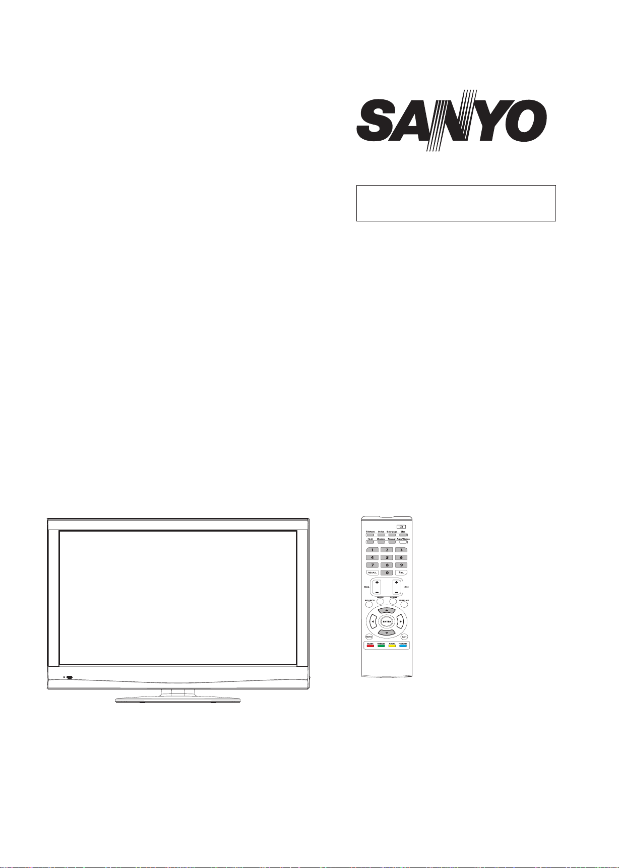
FILE NO.
SERVICE MANUAL
LCD TV
LCD-32XR9K
PRODUCT CODE No.
PRODUCT CODE No.
1 682 348 51: PAL/SECAM
NTSC(AV)
REFERENCE No.:SM0915077
Page 2

CONTENTS
Safety precautions…………………………………………………………………1
Alignment instructions……………………………………………………………..3
Software upgrade method…………………………………………………………8
Block diagram………………………………………………………………………10
IC block diagram……………………………………………………………………11
Troubleshooting guide……………………………………………………………..12
Schematic diagram………………………………………………………………...20
APPENDIX-A: Assembly list
APPENDIX-B: Exploded view
Page 3

Attention: This service manual is only for service personnel to take reference with. Before
servicing please read the following points carefully.
Safety precautions
1. Instructions
Be sure to switch off the power supply before replacing or welding any components or
inserting/plugging in connection wire Anti static measures to be taken (throughout the entire
production process!):
a) Do not touch here and there by hand at will;
b) Be sure to use anti static electric iron;
c) It’s a must for the welder to wear anti static gloves.
Please refer to the detailed list before replacing components that have special safety
requirements. Do not change the specs and type at will.
2. Points for attention in servicing of LCD
2.1 Screens are different from one model to another and therefore not interchangeable. Be sure to
use the screen of the original model for replacement.
2.2 The operation voltage of LCD screen is 700-825V. Be sure to take proper measures in
protecting yourself and the machine when testing the system in the course of normal operation or
right after the power is switched off. Please do not touch the circuit or the metal part of the module
that is in operation mode. Relevant operation is possible only one minute after the power is
switched off.
2.3 Do not use any adapter that is not identical with the TV set. Otherwise it will cause fire or
damage to the set.
2.4 Never operate the set or do any installation work in bad environment such as wet bathroom,
laundry, kitchen, or nearby fire source, heating equipment and devices or exposure to sunlight etc.
Otherwise bad effect will result.
2.5 If any foreign substance such as water, liquid, metal slices or other matters happens to fall into
the module, be sure to cut the power off immediately and do not move anything on the module lest
it should cause fire or electric shock due to contact with the high voltage or short circuit.
2.6 Should there be smoke, abnormal smell or sound from the module, please shut the power off
at once. Likewise, if the screen is not working after the power is on or in the course of operation,
the power must be cut off immediately and no more operation is allowed under the same
condition.
2.7 Do not pull out or plug in the connection wire when the module is in operation or just after the
power is off because in this case relatively high voltage still remains in the capacitor of the driving
circuit. Please wait at least one minute before the pulling out or plugging in the connection wire.
2.8 When operating or installing LCD please don’t subject the LCD components to bending,
twisting or extrusion, collision lest mishap should result.
2.9 As most of the circuitry in LCD TV set is composed of CMOS integrated circuits, it’s necessary
to pay attention to anti statics. Before servicing LCD TV make sure to take anti static measure and
ensure full grounding for all the parts that have to be grounded.
2.10 There are lots of connection wires between parts behind the LCD screen. When servicing or
moving the set please take care not to touch or scratch them. Once they are damaged the screen
1
Page 4
would be unable to work and no way to get it repaired.
If the connection wires, connections or components fixed by the thermotropic glue need to
disengage when service, please soak the thermotropic glue into the alcohol and then pull them
out in case of dagmage.
2.11 Special care must be taken in transporting or handling it. Exquisite shock vibration may lead
to breakage of screen glass or damage to driving circuit. Therefore it must be packed in a strong
case before the transportation or handling.
2.12 For the storage make sure to put it in a place where the environment can be controlled so as
to prevent the temperature and humidity from exceeding the limits as specified in the manual. For
prolonged storage, it is necessary to house it in an anti-moisture bag and put them altogether in
one place. The ambient conditions are tabulated as follows:
Temperature Scope for operation 0 ~ +50 oC
Scope for storage -20 ~ +60 oC
Humidity Scope for operation 20% ~ 85%
Scope for storage 10% ~ 90%
2.13 Display of a fixed picture for a long time may result in appearance of picture residue on the
screen, as commonly called “ghost shadow”. The extent of the residual picture varies with the
maker of LCD screen. This phenomenon doesn’t represent failure. This “ghost shadow” may
remain in the picture for a period of time (several minutes). But when operating it please avoid
displaying still picture in high brightness for a long time.
3. Points for attention during installation
3.1 The front panel of LCD screen is of glass. When installing it please make sure to put it in
place.
3.2 For service or installation it’s necessary to use specified screw lest it should damage the
screen.
3.3 Be sure to take anti dust measures. Any foreign substance that happens to fall down between
the screen and the glass will affect the receiving and viewing effect
3.4 When dismantling or mounting the protective partition plate that is used for anti vibration and
insulation please take care to keep it in intactness so as to avoid hidden trouble.
3.5 Be sure to protect the cabinet from damage or scratch during service, dismantling or
mounting.
2
Page 5
Alignment Instructions
1. Alignment equipments
Digital Multimeter
Signal Generator (54200)
Personal Computer (FLASH writing tool pre-installed)
VG848 & VG849 (VGA, YPbPr, HDMI signal generator)
DVD player with HDMI jack
CA210 (white balancer)
Monitor
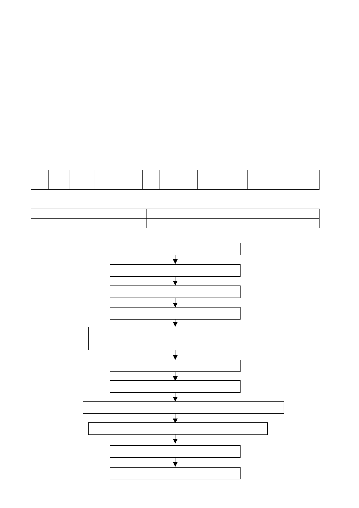
2. Power voltage test and alignment flow chart
2.1 Power voltage test
According to wiring diagram connect all boards correctly. Connect power and press POWER button
to turn on the TV.
a) In turn measure XJ01 all pin voltage. The data is shown below (Table 1).
Table 1: XJ01 all pin voltage
XJ01 Pin1 2 3
Voltage >2.5 V 0~3.3 V 0 11.4 V~12.6 V 0 31.4 V~32.6 V 4.75 V~5.25 V 0 4.75 V~5.25 V 0 >2.5 V
b) In turn measure XV04 all pin voltage, the data is shown below (Table 2).
XV04 Pin1 2 3 4 5
Voltage
22.8 V~25.2 V 22.8 V~25.2 V
4、5 6、7
Table 2 XV04 all pin voltage
8 9 10 11 12 13
0 0 0
2.2 Alignment flow chart (Fig.1)
Check if DDC, FLASH, KEYis written
Data process board making
Complete set alignment
White balance alignment
Input signal and check all TV function (no lost program, analog
control be normal). Check earphone and speaker output is normal.
Check if AV/SVIDEO/SCART input is normal
Check if YPbPrinput is normal
Check if VGA input is normal. Check VGA mode analog control, H/V-center, etc.
Check if HDMI input is normal. Check all the function at this mode.
Defaults preset
Check accessory, then pack the TV
3
Page 6

3. Alignment instructions
3.1 Complete set alignment
3.1.1 According to wiring diagram connect all boards correct ly. Power on the TV, check if the display
is normal.
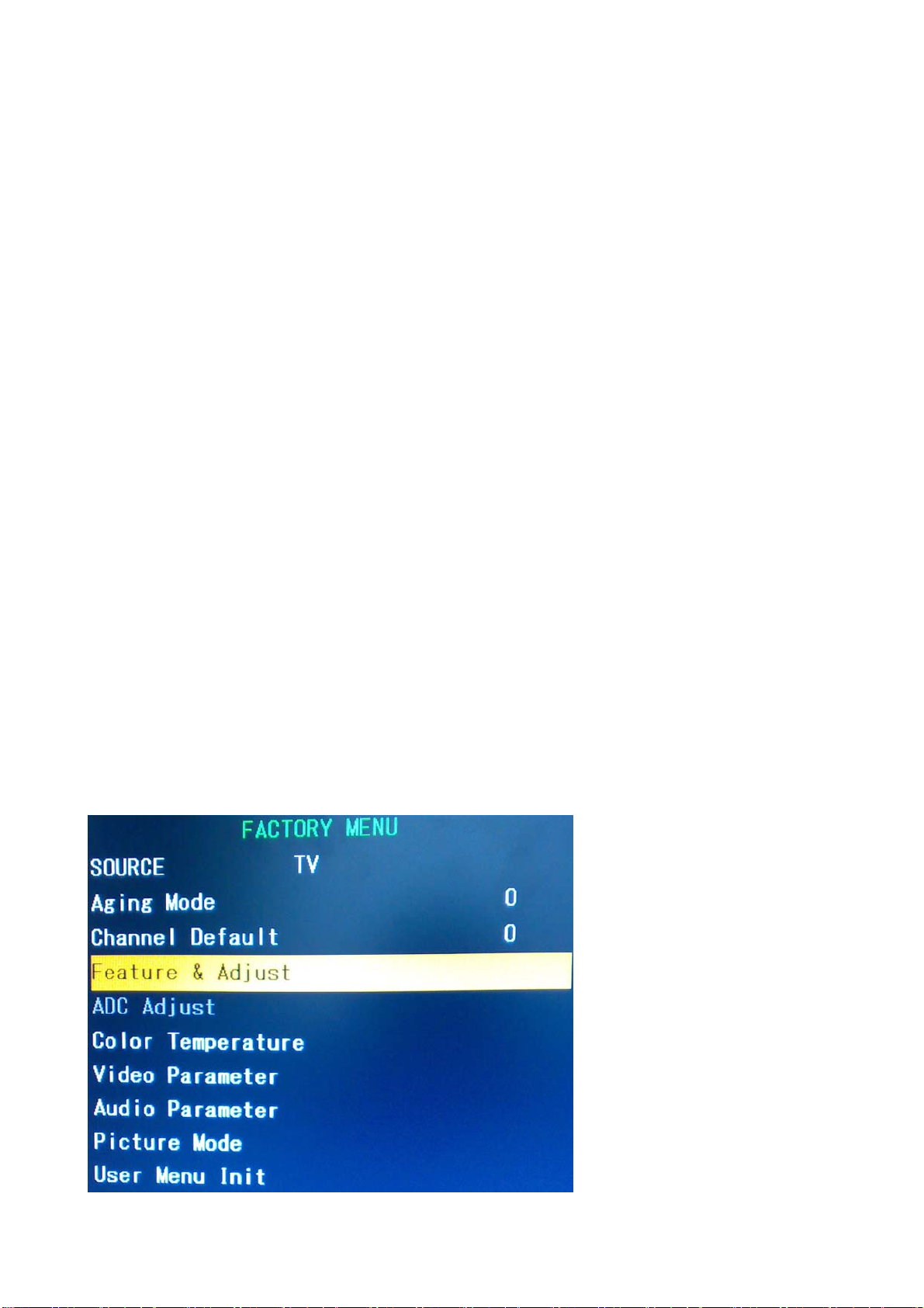
3.1.2 Factory menu usage
a) First press “INPUT” button, then in turn press “2、5、8、0” to access factory main menu.
b) Press “” and “” to select item, then press “” to access.
c) Press “” and “” to move upward or downward and select item.
d) Press “” and “” to adjust.
e) Press “MENU” to return to the previous screen.
3.2 White balance adjustment
3.2.1 Preparations before adjustment
Before white balance adjustment, let the TV work for more than 30 minutes so the TV will be in
stable status. Then use white balancer CA210 to adjust.
a) When adjusting in VGA mode, input VESA800×600/60Hz (for VG848 Timing, input 854) format
signal with crosshatch pattern. Go to user menu, select VGA Settings from Setup menu, then select
Auto to perform auto correction so that the picture can be displayed wholly. Then input signal from
VG848 with PATTERN of 914, go to factory menu and select ADC ADJUST to perform AUTO ADC
until “Complete” appears.
b) When adjusting in YPbPr mode, first input 480i/60 Hz format signal with 75% color bar plus gray
scale (VG848 Timing, input 968, PAT 918). Go to factory menu, select ADC ADJUST to perform
AUTO ADC until “Complete” appears.
c) In this chassis only perform NORMAL color temperature alignment. During alignment please
guarantee that bright step’s color temperature to be △X≤±5, △ Y≤±5, dark step color
temperature to be △X≤±10, △Y≤±10. Depending on different LCD panel type (non-TN panel
& TN panel), the color temperature requirement is different. See below table 3.
Panel type Cool Normal Warm
Non-TN panel 12000K(272、278) 9300K(285、293) 6500K(313、329)
TN panel 10000K(280、288) 8000K(295、305) 6500K(313、329)
Table 3: Color temperature requirements
4
Page 7

3.2.2 Four channels white balance adjustment
3.2.2.1 For AV channel (TV/S-VIDEO/SCART is the same)
Through AV channel, input 8-step gray scale signal (VG848 Timing, input 969, PAT 920), go to
factory menu and access Color Temperature menu page, fix G-GAIN, adjust R-GAIN and B-GAIN to
th
make the 7
B-OFFSET to make the 2
adjust R-GAIN, B-GAIN and R-OFFSET, B-OFFSET until both the first and second steps’
chromaticity coordinates be (285, 293).
3.2.2.2 For DVI channel (HDMI is the same)
Through DVI channel, input 8-step gray scale signal (VG848 Timing input 854, PAT 920), go to
factory menu and access color temperature menu page, fix G-GAIN, adjust R-GAIN and B-GAIN to
make the 7
B-OFFSET to make the 2
step chromaticity coordinates be (285, 293). Fix G-OFFSET, adjust R-OFFSET and
nd
step chromaticity coordinates be (285, 293). In this way repeatedly
th
step chromaticity coordinates be (285, 293). Fix G-OFFSET, adjust R-OFFSET and
nd
step chromaticity coordinates be (285, 293). In this way repeatedly
adjust R-GAIN, B-GAIN and R-OFFSET, B-OFFSET until both the first and second steps’
chromaticity coordinates be (285, 293).
3.2.2.3 For YPbPr channel
Through YPbPr channel input 8-step gray scale signal (VG848 Timing, input 968, PAT 920), go to
factory menu and access color temperature menu page, fix G-GAIN, adjust R-GAIN and B-GAIN to
th
make the 7
B-OFFSET to make the 2
step chromaticity coordinates be (285, 293). Fix G-OFFSET, adjust R-OFFSET and
nd
step chromaticity coordinates be (285, 293). In this way repeatedly
adjust R-GAIN, B-GAIN and R-OFFSET, B-OFFSET until both the first and second steps’
chromaticity coordinates be (285, 293).
3.2.2.4 For VGA channel
Through VGA channel input 8-step gray scale signal (VG848 Timing, input 854, PAT 920), go to
factory menu and access color temperature menu page, fix G-GAIN, adjust R-GAIN and B-GAIN to
th
make the 7
B-OFFSET to make the 2
step chromaticity coordinates be (285, 293). Fix G-OFFSET, adjust R-OFFSET and
nd
step chromaticity coordinates be (285, 293). In this way repeatedly
adjust R-GAIN, B-GAIN and R-OFFSET, B-OFFSET until both the first and second steps’
chromaticity coordinates be (285, 293).
5
Page 8
4. Performance check
4.1 TV function check
Input RF signal. Open the user menu and first go to Channel menu, perform auto scan to check if
there is any program lost. Check speaker output normally and picture is displayed normally.
4.2 AV/SVIDEO/SCART input check
Respectively input signal through AV/SVIDEO/SCART, check if picture and sound are normal.
4.3 YPbPr/YCbCr input check
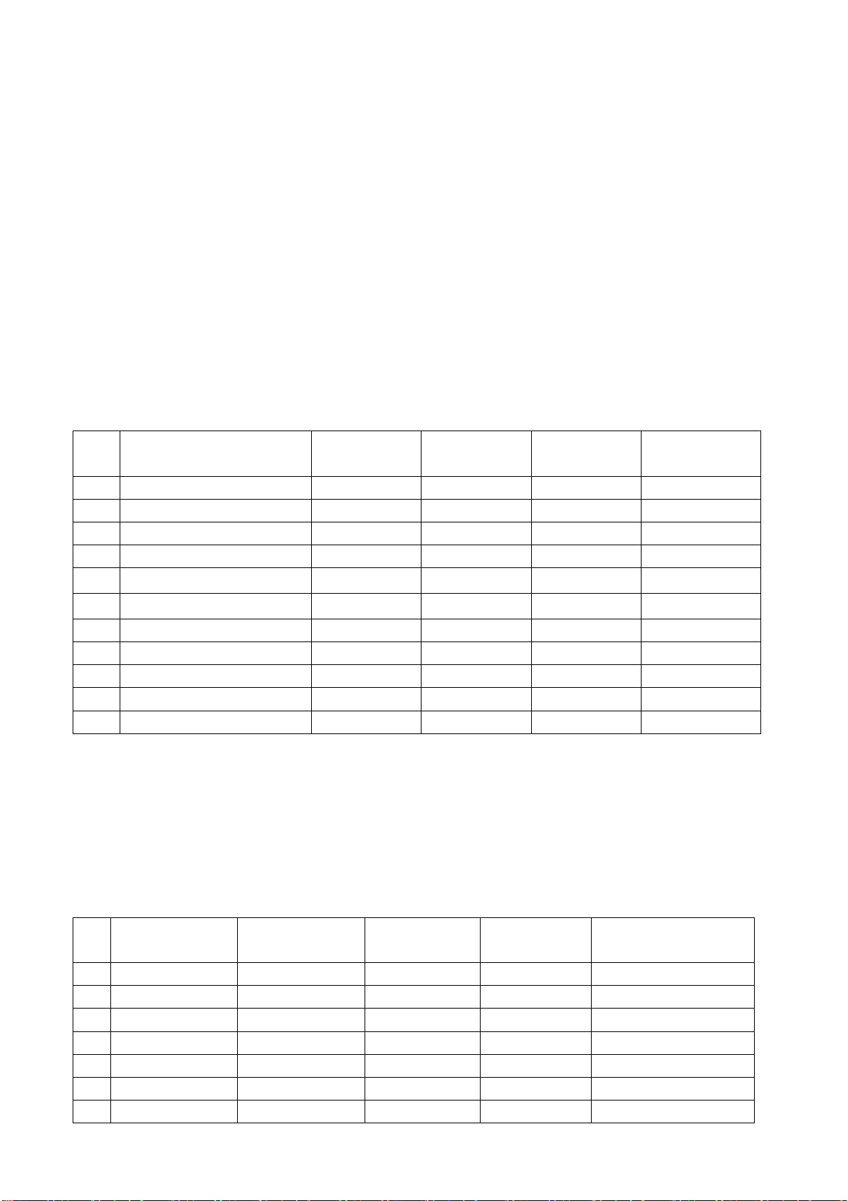
Respectively input all format YUV signal (shown at below table 4) by VG848 signal generator and
check picture display and sound are normal.
Table 4: Component (YUV) signal format
# Resolution
712×484@59.94/60 Hz
1
702×574@50Hz
2
720×483p@59.94/60 Hz
3
720×576p@50 Hz
4
1280×720@50 Hz
5
1280×720p@59.94/60 Hz
6
H-freq.
kHz
15.734 59.94/60 13.50 480i(59.94/60p)
15.625 50 13.50 576i/50
31.469 59.94/60 27.00 480p(59.94/60p)
31.25 50 27.00 576p/50
37.50 50 74.25 720p/50
44.96 59.94 74.18 720p(59.94/60p)
V-freq.
Hz
Dot-clock freq.
MHz
Remarks
7
1920×1080i@50Hz
1920×1080i@59.94/60 Hz
8
1920×1080p@23.98/24 Hz
9
1920×1080p@50Hz
10
1920×1080p@59.94/60 Hz
11
28.125 50 74.25 1080i/50
33.75 59.94 74.25 1080i(59.94/60i)
27.00 23.98/24 74.25 1080p(23.98/24p)
56.25 50 148.50 1080p/50
67.50 60.00 148.50 1080p(59.94/60p)
4.4 VGA input check
Respectively input all format VGA signal (shown at below table 5) by VG848 signal generator.
Check if the display and sound are normal. If picture has deviation in horizontal and vertical
direction, perform auto correction by making use of Setup menu/VGA Settings/Auto item.
Table 5: PC signal format
# Resolution
1
720×400@70 Hz
2
640×480@60 Hz
3
640×480@72 Hz
4
640×480@75 Hz
5
800×600@60 Hz
6
800×600@70 Hz
7
800×600@75 Hz
31.47 70.08 28.32 DOS
31.50 60.00 25.18 VESA
37.90 72.00 31.50 VESA
37.50 75.00 31.50 VESA
37.90 60.00 40.00 VESA
46.90 72.19 49.50 VESA
48.08 75.00 50.00 VESA
H-freq.
kHz
V-freq.
Hz
Dot-clock freq.
MHz
Remarks
6
Page 9

8
1024×768@60 Hz
9
1024×768@70 Hz
10
1024×768@75 Hz
11
1360×768@60 Hz
48.40 60.00 65.00 VESA
56.50 70.00 75.00 VESA
60.00 75.00 78.75 VESA
47.71 60.01 85.50 VESA
4.5 HDMI input check
Respectively input all format HDMI signal (shown at below table 6) by VG849 signal generator,
check if picture display and sound are normal.
Table 6: HDMI signal format
# Resolution H-freq. (kHz) V-freq. (Hz)
712×484@59.94/60 Hz
1
2
3
4
5
6
7
8
9
10
11
702×574@50Hz
720×483p@59.94/60 Hz
720×576p@50 Hz
1280×720@50 Hz
1280×720p@59.94/60 Hz
1920×1080i@50Hz
1920×1080i@59.94/60 Hz
1920×1080p@23.98/24 Hz
1920×1080p@50Hz
1920×1080p@59.94/60 Hz
15.734 59.94/60 13.50 480i(59.94/60p)
15.625 50 13.50 576i/50
31.469 59.94/60 27.00 480p(59.94/60p)
31.25 50 27.00 576p/50
37.50 50 74.25 720p/50
44.96 59.94 74.18 720p(59.94/60p)
28.125 50 74.25 1080i/50
33.75 59.94 74.25 1080i(59.94/60i)
27.00 23.98/24 74.25 1080p(23.98/24p)
56.25 50 148.50 1080p/50
67.50 60.00 148.50 1080p(59.94/60p)
Note: A DVI device also can be connected to the HDMI jack by using a DVI to HDMI adapter cable.
About supported DVI signal format, please refer to table 5 PC signal format and table 6.
Dot-clock freq.
MHz)
Remarks
4.6 HDMI sound supporting format
HDMI sound only supports PCM format, its sample rate supports 32 KHz, 44 KHz and 48 KHz.
5. Default setting for user menu
Go to factory menu “User Menu Init” item, press ENTER button on the remote control, then the TV
will preset all settings to default. After factory alignment, this step must be done surely.
6. Packing
Check accessory then pack the TV.
7
Page 10
Software upgrade method
1 Using USB port to upgrade (it is suggested to use this method in preference)
1.1 Precautions
The upgrade file must be saved under root category of USB device, and the file name must be
changed to “KU19P.BIN” or “ku19p.bin”.
1.2 Upgrade steps:
a) Copy the provided “KU*.bin” file to USB device root category. Then change the file name to
“ku19p.bin” or “KU19P.BIN”.
b) Completely cut off the TV power by unplug the power cord from the power outlet. (Be sure to use
buttons on the remote control or on the TV to completely discharge the TV after power off).
c) Insert the USB device into the USB port. Keep holding any button (except POWER button) on the
TV and then plug the power cord into the power outlet, after about 2-3s release the button, the
software begins to upgrade automatically. Note that during upgrade the USB device can not be
removed and the TV can not be power off.
d) During the process operate according to hints provided on the screen. When complete, remove
the USB device, unplug the power cord and then plug it again, then press POWER to turn on the
TV.
e) After software upgrade the TV must be performed initialization and ADC correction and white
balance alignment again. Below are steps for initialization:
ⅰ. Go to factory menu, select the third item “Feature & Adjust”.
8
Page 11
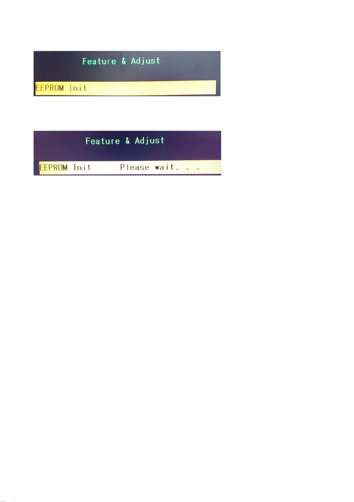
ⅱ. Go to “Feature & Adjust” sub-menu, select “EEPROM Init” at the first line.
ⅲ. Press “” (RIGHT arrow button) to perform initialization. During the process the message
“Please Wait” will be displayed. When complete, “OK” is displayed.
9
Page 12
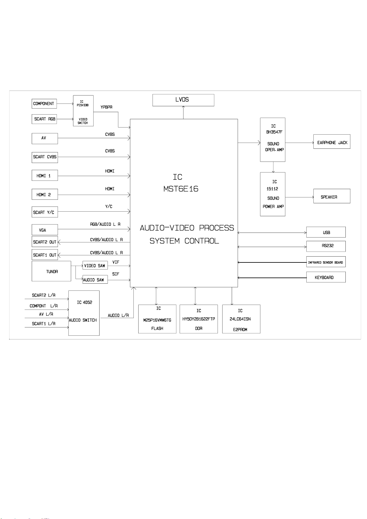
Block Diagram
10
Page 13

IC block diagram
GENERAL DESCRIPTION
The MST6E16GS is a high performance and fully integrated IC for multi-function LCD monitor/TV
with resolutions up to full HD (1920x1080). It is configured with an integrated triple-ADC/PLL, an
integrated DVI/HDCP/HDMI receiver, a multi-standard TV video and audio decoder, a video
de-interlacer, a scaling engine, the MStarACE-3 color engine, an on-screen display controller, an
8-bit MCU and a built-in output panel interface. By use of external frame buffer, PIP/POP is
provided for multimedia applications. Furthermore, 3-D video decoding and processing are
fulfilled for high-quality TV applications. To further reduce system costs, the MST6E16GS also
integrates intelligent power management control capability for green-mode requirements and
spread-spectrum support for EMI management.
11
Page 14

Troubleshooting Guide
Common-trouble judging flow chart
Connect the power.
Check if power supply or
infrared sensor board has trouble,
Check if the indicator
lights red.
Yes, then press
POWER button.
Check if the indicator
lights blue.
Yes
Check if the screen
lights up.
No
or power cord problem.
Check if main chip (MST6E16)
pin44 waveform is sine wave,
FLASH pin6 waveform is square-
No
wave. Check main chip peripheral
circuit and FLASH/EEPROM
peripheral circuit.
Check backlight board, then
No
check main chip pin81 backlight
control status.
Yes
Check if every source
video display is normal.
Check if every source
sound is normal.
Check if signal from its
input to IC pin is normal. If
No
normal, then check IC and
its periphery, and LVDS
output.
No
Check if signal from its
input to IC pin is normal.
If normal, then check IC
and its periphery
12
Page 15

1. No raster (screen is not lit), no picture, no sound
No raster,
no picture & sound
Check if indicator lights up.
Check if indicator
lights blue.
No
Check main chip
pin 156 LED
control status.
Check main chip and
FLASH periphery.
Check NS01 pin 44 waveform
is sine wave or not.
Yes
Check main chip
(NS01), FLASH
(NS02) power.
NormalAbnormal
Check if main chip pin169
(reset receiving signal) is of
low level.
Yes No
Check NS01, confirm NS01
has reset correctly.
NoYes
Check circuit of
infrared sensor board.
Check Standby _ 5V
Normal Abnormal
Disconnect power
board and Data
process board, then
test Standby _ 5V
again.
Normal
Abnormal
Power board
exists
problem.
No
Check NS01 crystal
oscillator circuit.
Yes
Check NS01, NS02, NS04,
NS05 and its periphery.
Note: If detect NS01 (main chip) pin 169 is of high level, you may remove RS14, detect VS01
emitter if first output high level after power on, then output low level continuously. If not, the reset
circuit may have problem. First detect if NS01 (main chip) pin 44 waveform is sine wave, if not,
check NS01 crystal oscillator circuit. When checking periphery of NS01, NS02 and NS05, check
relative component’s welding, then use oscilloscope to detect the joint resistor pin between NS01
and NS05. If the waveform is not regular square-wave, that means either NS01 or NS05 work
abnormally and therefore cause address line and data line be in error. NS05 error probability is
greater. In addition, if joint resistor between NS01 and NS05 is in error, it will also cause no raster,
no picture and no sound.
13
Page 16

2. Sound normal, but no picture
(blue screen and OSD can be displayed.)
Sound is OK,
but no picture.
Check backlight
is lit.
Yes No
Try other source, to
check the picture
display.
Yes No
Check NS01
and its
periphery.
Note: HDMI channel is excluded. For HDMI channel picture and sound check, please refer to procedure
of 5.
Check according to
steps of 4. Picture
OK, but no sound.
Check backlight
board, main chip pin
81 backlight control
status.
3. Sound OK, but no picture (only backlight lights up)
Sound is ok, but
only raster appears.
Check LVDS power
supply is normal.
Check signal from NS01
to XS01 is normal.
Normal Abnormal
Panel LVDS
reception board
has problem.
Check N402 circuit.
Normal Abnormal
Check NJ05 pin 2 is
low level or not.
Check NS01 power
supply and its
peripheral circuit.
Yes No
Check NS01 pin 162
and its inverter circuit.
14
Page 17

4. Picture normal, but no sound
No
Picture is OK,
but no sound.
Check main
board XV05 has
signal output.
Yes
Check power amplifier
relative pins have squarewave signal output.
Check power
amplifier rear
stage peripheral
circuit.
Check NV06
corresponding
channel has signal
input.
Speaker problem
NoYes
Check CV18,
CV22 have signal
input amplification.
YesNo
Check power
amplifier’s peripheral
circuit, the power
supply and MUTE pin
circuit.
Yes No
Check NV06
peripheral circuit
and its power
supply.
Check every stage
circuit along the
audio input channel
15
Page 18

4. Some source channel work abnormally.
a) AV1 channel has no picture
Check CS30 has
signal input.
Yes
Check NS01 peripheral
circuit, crystal oscillator
and its power supply.
b) channel has no picture
SCART CVBS
Check CS28 has
signal input.
Yes No
Check NS01 peripheral
circuit, crystal oscillator
and the power supply.
No
The route from AV 1
socket to NS01 exists
problem.
The route from SCART
CVBS socket to NS01
exists problem.
c)
SCART Y/C
Check NS01 peripheral
circuit, crystal oscillator
and the power supply.
channel has no picture
Check CS25, CS26
has signal input.
Yes No
The route from SCART
Y/C socket to NS01
exists problem.
16
Page 19

d) TV channel has no picture
Check LJ31 has
signal input.
Check NS01
peripheral circuit,
crystal oscillator and
the power supply.
e)
YPbPr/SCART RGB
Yes
Check circuit
between
TUNER1 and
NS01.
channel has no picture
No
Check TUNER1 pin
11 has signal output.
NoYes
Check TUNER1
peripheral
circuit, power
supply and bus.
Check NS01 peripheral
circuit, crystal oscillator
and the power supply.
Check NB06 pin 2,
pin 5, pin 11/3, pin 6,
pin 10 have signal
input.
No Yes
The route between
YPbPr/SCART RGB
socket and
NB06 exists problem.
Check CS21, CS22, CS23,
CS24 have signal input.
Yes No
Check NB06 pin 4, pin 7,
pin 9 have signal output.
No Yes
Check channel
between NB06
output and NS01
input.
Check NB06
peripheral circuit,
the power supply.
17
Page 20

e) VGA channel has no picture
Check NS01 pin 29,
pin 30 have
synchronous signal
input.
Yes
Check CS17, CS18, CS19,
CS20 have signal input.
Yes No
Check NS01
circuit.
Check circuit
between VGA
socket and NS01.
f) HDMI channel has no picture
Check NS01 has digital
signal input.
No
Check circuit
between VGA
socket and NS01.
Yes No
Check NS01 peripheral
circuit, crystal oscillator
and the power supply.
Check circuit between
HDMI socket and
NS01.
Note: To get normal HDMI picture, especially when connect to DVD player with HDCP
information, it must be guaranteed that NV04 and NV05 (HDMI port DDC chip) writing
is correct, and especially bus between NV04, NV05 and HDMI jack must be smooth
and unhindered. Secondly HOTPLUG circuit must be guaranteed (it is of high level at
normal broadcast), otherwise the picture playback can not be normal.
18
Page 21

g) HDMI channel has no sound
Check NS01 has
digital signal input.
Yes
Check NS01 peripheral
circuit, crystal oscillator
and the power supply.
No
Check circuit between
HDMI socket and NS01.
Note: To get normal HDMI sound , especially when connect to DVD player
with HDCP information, it must be guaranteed that NV04 and NV05 (HDMI
port DDC chip) writing is correct, and bus between NV04, NV05 and HDMI
jack must be smooth and unhindered, otherwise the sound playback can
not go
.
19
Page 22

Power Switch
Wiring diagram
Page 23

100n
CB16
5
BC847AW
VB03
RB84
47
RB86
8.2K
10K
2.2u
SC2_R
BC847AW
RB102
VB08
47
RB110
8.2K
SC2_L
HD2_Y
HD2_Pb
HD2_Pr
YPbPr_SOUND 1/2
HJR-413/PB-1
XB02
R1
L1
3
1
330p
CB15
PESD5V0L5UY
NB07
RB60
10K
12K
RB62
560p
CB23
HD1_RIN
SCART2_R
4.7K
CB39
SCART2_L
4.7K
RB109
330p
RB61
12K
CB22
560p
RB83
+12V
100n
RB101
+12V
CB46
100n
1234
6
RB85
47K
RB87
CB40
47K
RB111
10K
2.2u
CB47
11
12 13 14
67
1
234
RB24
RB2547RB23
47
VGA_R
VGA_G
R2
NB09
RB146
100
2.2u
CB60
RB1670RB168
0
SCART2_L
SCART2_VOUT
VGA AUDIO
JY-3541L-01-030
XB06
RB105
10K
12K
RB114
RB113
560p
CB51
PC_LIN
VGA
89
47
SOG
VGA_B
B2
CB29
RB157
0
RB92
150
27K
RB95
BC847AW
VB05
BC847AW
R
G
L
RB104
10K
GND-H
12K
560p
CB50
PC_RIN
15
10
RB27
470
SCART2_VOUT
RB69
470u
BC857AW
VB11
RB96
100
27K
RB97
VB06
4.7K
RB98
GAIN_SW
1
3
4
5
GND-H
5
RB22
2.2K
2.2K
RB26
DDC_SDA
G2
75
16V
BC857AW
VB01
RB70
200
RB71
270
BC847AW
VB04
10u
CB43
CVBSOUT2
PESD5V0L4UG
NB11
100n
CB48
CB49
100n
HC1038-15F-3.08
XB07
RB14
100
HS_RGB
DDC_SCL
R1
RB49
0
RB63
RB64
12K
560p
CB24
100n
CB27
470
RB156
330
RB88
100K
RB89
2
PESD5V0L4UG
2
RB154
47
SV1_YIN
SV1_CIN
5
6
1
3
4
5
RB13
100
VS_RGB
AV IN
B1
RB48
0
AV1_R
10K
+12V
RB68
12K
560p
CB28
AV1_RIN
S1_VIDEO
HJK-3.5-401
G
XB05
G
G
RB103
75
RB112
75
NB12
1
3
4
5
NB17
2
CB55
100n
RB153
47
PESD5V0L5UY
NB01
PESD5V0L4UG
NB04
2
100n
CB03
G1
RB47
0
AV1_L
CB25
330p
RB65
75
RB67
10K
47
AV1_VIN-
AV1_LIN
I2C_UPDATE
C
Y
S
1
3
4
5
TX0
RX0
34
2
1
RB148
G
NC
RB66
R
RB129
100
RXD0
100n
CB01
RB46
0
47
AV1_VIN+
L
RB128
100
TXD0
AV13-06-526
XB03
YPBPRIN
HJR-613/PB-1
R2
B2
G2
RB09
RB10
0
RB11
RB12
75
75
CB09
CB10
2.2u
2.2u
1
4
3
5
PESD5V0L4UG
2
100n
CB11
R2
4
CB14
HD1_LIN
6
2
CB13
330p
RB59
RB54
10K
10K
RB58
12K
560p
CB21
HD2_R
HD2_RIN
BC847AW
VB02
RB79
47
RB81
8.2K
SC1_R
BC847AW
RB100
VB07
47
RB107
8.2K
SC1_L
25V
NB05
47K
RB44
47K
RB45
L2
5
CB12
330p
RB56
10K
RB57
12K
CB20
560p
HD2_L
HD2_LIN
SCART1_R
RB80
47K
RB82
10K
2.2u
CB38
SCART1_L
RB106
47K
RB108
10K
2.2u
CB45
AU_SW1
RB78
4.7K
+12V
CB37
100n
RB99
4.7K
+12V
CB44
100n
0
25V
8
GND
IN
1
1K
RB1620RB163
0
europe
china
AU_SW0
RB04
0
RB08
75
CB08
10V
47u
RB41
47K
RB43
47K
13
15
S2D14S1D
EN
DD
12
RB55
11
12
B1
R1
HD1_Pb
HD1_Pr
RB07
75
RB06
75
CB07
CB06
2.2u
2.2u
25V
25V
47K
RB42
47K
10
5
S1B6S2B
S2C11S1C
PI5V330
NB06
DB
DC
7
9
RB53
RB52
47
PR+
SCART2 (CVBS+YC)IN/MONITOROUT
10
470
47
SOY
PB+
RB40
RB51
RS232
470n
CB63
470n
CB64
100n
CB65
1
C1+2V+3C1-4C2+5C2-6V-7T2OUT8R2IN
MAX3232CSE
NB18
R1OUT
T1OUT
R1IN
GND16Vcc
12
13
14
15
+5V_STB
RB159
RB158
100
100
CB70
10u
SCART2_ROUT
SCART2_LOUT
0
HD2_L
CB67
100n
30p
CB68
30p
CB69
TX0
RX0
RB144
HD2_R
8.2K
RB127
RB141
1.5K
RB155
RB145
0
SC2_FS
SCART2_VOUT
TXD0
R2OUT
RB161
0
T2IN11T1IN
9
RB160
RXD0
CB66
470n
10
0
G1
75
CB05
S1A3S2A
DA
Y+
0
RB05
47u
2
4
47
3456789
47
RB150
VCC
RB50
HD1_Y
10V
16
100n
25V
10u
CB19
CB36
100n
PESD5V0L4UG
NB10
AV2_L
1
2
0
RB125
RB126
SV1_CIN
SV1_YIN
XB01
RB38
47K
CB18
STPB3216-310PT
RCA-302A-01
2
AV2_R
XB09
TJC10-12A
0
RB133
0
1
4
3
5
CB04
100n
RB32
47K
LB01
NB03
PESD5V0L4UG
2
RB34
RB36
RB35
RB37
47K
47K
47K
47K
+5V
R
XB04
5
4
3
RB152
1
0
AV2_R
RB72
RB73
10K
RB75
RB74
12K
12K
560p
560p
CB35
CB34
AV2_RIN
HJ-2105F
XB08
6
PESD5V0L5UY
NB14
SCART1
2
1
1R_OUT31L_OUT5GND-D71B_IN9GND-D111G_IN13GND-D151RED_IN
1R_IN4GND-D61L_IN81FUN_SEL10@pinCo12@pinCo14GND-D161RGB_SW17GND-D191TV_OUT18GND-D201TV_IN21GND-D
5
1234
100n
CB52
0
RB135
1n
1n
CB31
10K
RB91
100
2.2u
SCART1_R
0
CB30
RB132
10K
RB90
RB94
RB93
100
2.2u
CB42
CB41
AV2_L
SCART1_L
0
RB29
RB31
DDC_SDA
AV2
W
@pinCo
RB151
0
AV2_L
CB32
330p
10K
RB76
RB149
47
AV2_LIN
AV2_VIN-
R168,R169 CONNECT CHINA
RB122
8.2K
RB130
1.5K
0
RB131
SC_FS
AV2_R
SC_FS
MMBD1204
1AO2A13A24
GND
SDA6SCL
5
100
75
R167,R166 CONNECT EUROPE
24C02N-10SI27
NB02
Vcc
7WP8
100n
CB02
RB28
10K
10K
RB15
10K
RB17
RB30
100
RB33
100
RB39
100
TXD0
DDC_SCL
47
AV2_VIN+
RXD0
Y
YWR
@pinCo
CB17
100n
PESD5V0L4UG
2
NB08
CB33
100n
AV2_V
SCART2_LOUT
SCART2_ROUT
2
1n
CB72
10K
RB165
RB169
0
SCART1_R
5
6
RB77
1234
RB118
0
RB115
75
RB1200
HD2_Y
HD2_Y
HD2_Pr
0
RB119
HD2_Pr
RB134
75
CB56
100n
470u
CB62
16V
RB170
VB12
BC857AW
150
BC857AW
VB09
RB136
BC847AW
330
RB138
VB10
47
220
RB137
47K
16K
CB57
10u
RB139
RB140
CVBSOUT
0
RB121
HD2_Pb
HD2_Pb
5
4
3
1
RB147
100
2.2u
CB61
RB166
0
SCART2_R
PESD5V0L5UY
NB13
5V_TUNNER
SC_FB
5
4
3
1
0
RB116
AV2_V
75
RB16
75
RB18
75
RB21
PESD5V0L4UG
1n
CB71
10K
RB164
AV OUT
SCART1_L
+5V
DB01
Page 24

POWER IN
XJ01
TJC3-13A
1
BL_ON/OFF
2
PWM
3
GND
4
12V
5
12V
6
GND
7
GND
8
32V
9
5V
10
GND
11
5V_STB
12
GND
13
ON/OFF
RJ08
12K
10n
CJ09
RJ07
CJ10
6.8n
6.8K
ON_USB1
ON_PANEL
+12V
+5V_STB
RJ03
10K
+32V
CJ06
3.9n
RJ04
+5V
RJ05
30K
CJ11
470p
RJ01
+5V
DJ01
SK34A
DJ08
D1FS4
RJ06
1K
20K
CJ07
1u
LJ02
STPB3216-380PT
CJ126
100n
8
7
6
5
2K
RJ103
5V_ALL
1K
CJ01
100n
STPB3216-380PT
BC847AW
8
7
6
5
CJ08
470p
HP-MUTE
100n
SS
EN
COMP
FB
+5V_STB
RJ09
1K
VJ01
BC847AW
CJ12
2.2u
LJ03
STPB3216-380PT
LJ04
+5V_STB
RJ16
4.7K
RJ17
4.7K
VJ04
NJ03
MP1410-C019
N/C
EN
COMP
FB
CJ05
CJ04
10V
220u
NJ04
MP1484
GND_4
RJ13
1K
CJ13
100u
16V
CJ15
100u
16V
AP1117-ADJ
BS
IN
SW
CJ27
100u
25V
1
2
3
4
RJ102
GND
RJ111
27K
IN
GND-H
CJ14
100n
CJ16
100n
0
BC847AW
BS
IN
SW
+12V
+5V_STB
RJ14
220
VJ03
BC847AW
AZ1084S-3.3
Vin
RJ100
4.7K
VJ17
5V_ALL
1
2
3
4
CJ22
100u
10V
10K
RJ112
NJ02
OUT
LJ06
STPB3216-380PT
CJ29
10n
CJ28
100n
5V_TUNNER
NJ01
Vout
ADJ/GND
GND-H
RJ101
4.7K
LJ05
STPB3216-380PT
CJ25
10n
SLF7032T-100M1R4-PF
1
CJ24
DJ03
MBRS130T3
10u
CJ23
100n
RJ110
10u
CJ123
RJ22
10K
LJ08
SLF12575T-220M4R0
1
CJ30
DJ04
470u
MBRS130T3
25V
LJ07
+5V
10K
VJ19
BC847AW
RJ19
470
RJ20
510
2
CJ17
100n
RJ21
20K
2
CJ26
470u
10V
CJ31
100n
RJ97
RJ12
4.7K
RJ24
4.7K
CJ19
100u
16V
PW_CTL
GND-H
CJ35
100n
VJ20
BC857AW
1K
RJ109
CJ21
220u
10V
RJ23
45.3K
STPB3216-380PT
STPB3216-380PT
4.7K
RJ98
4.7K
ON_PBACK
PWM2
LJ09
STPB3216-380PT
10u
CJ33
RJ25
820
VCC_1.26
CJ36
10u
+5V_EOP
+2.6VM
LJ10
STPB3216-380PT
CJ34
100n
LJ12
LJ13
+5V
RJ99
10K
+3.3V_STB
+5V_USB
+5V_PANEL
VJ16
BC847AW
AGC
SAS
SCL
SDA
TUNJ01
BP_+5V
NC7
VT_33V
NC9
NC10
TDQ-10A/126D
RJ26
1K
CJ59
100n
CJ71
100n
CJ70
10V
100uF
RJ40
560
+5V_USB1
+2.6VM
VCC_1.26
CJ60
100n
CJ72
100n
RJ108
0
BG2012D151T
STPB3216-380PT
5V_TUNNER
RJ38
10K
CJ74
RJ41
10n
10K
5V_TUNNER
RJ42
10K
CJ75
RJ43
10n
10K
LJ28
LJ29
GND-H
CJ61
100n
CJ73
1u
CJ76
1u
+2.6MVDD
CJ62
100n
VDDC
CJ63
2.2u
5V_TUNNER
RJ44
6.8K
LJ31
0.56uH
CJ64
100n
CJ65
100n
CJ84
CJ80
CJ78
CJ82
100n
100n
100n
100n
CJ85
CJ81
CJ79
CJ83
100n
100n
100n
100n
ZJ01
K9656
12345
RJ45
0
DJ06
MA859
VJ09
BC847AW
RJ49
0
12345
ZJ02
K3953
10p
CJ107
10p
CJ108
RJ50
10K
BC847AW
DJ07
+5V_USB1
RJ69
CJ120
12345
ZJ06
K9656
D3502H
EQ_AMP_F/B
IF_AGC2
IF_AGC1
VIF_in2
VIF_in1
GND
QIF_in
RF_AGC
AFT
Lofic_Vcc
Ref_Signal
Audio_Level_Cont.
Logic_GND
RJ64
100K
10n
NJ10
M61111FP
Video_det_out
51K
KEY&IR
Video_out
TV/FM_SW
Video_in
Vcc
APC
VCOF/B
SIF_in
Vreg
SIF_out
Audio_out
USB1_OC_DET
USB1_D+
USB1_D-
IR_IN
LED
5V_TUNNER
RJ104
2.7K
CJ116
10n
RJ106
2.7K
10n
CJ117
0
RJ47
CJ86
1200p
27p
GJ01
CJ87
RJ48
5V_TUNNER
4MHz
CJ88
150p
SIFP
SIFM
SIF_CTL
LJ32
STPB3216-310PT
CJ89
100n
5V_TUNNER
RJ59
2.2K
RJ60
2.2K
VIFM
VIFP
GND-H
GND-H
VJ12
BC847AW
RJ61
2.2K
CJ90
10V
47u
CJ96
100n
0
SIF_CTL
RJ51
10K
RJ52
10K
NC
RJ53
10K
5V_TUNNER
VJ10
RJ54
10K
RJ57
2.2K
VJ11
BC847AW
RJ58
4.3K
1u
RJ105
2.7K
5V_TUNNER
1u
CJ119
RJ107
GND-H
2.7K
GND-H
10n
CJ97
RJ66
4.7K
RJ65
100
ZJ05
12345
CJ118
GND-H
CJ92
10n
220n
CJ93
CJ94
10n
CJ95
100n
100n
CJ91
GND-H
GND-H
M9370M30
24
23
22
21
20
19
18
17
16
15
14
13
GND-H
VJ13
BC847AW
RJ67
10K
RJ68
30K
FUJ01
SMD1206P075TF
750mA
10V
100u
CJ114
XJ02
USB3112
100n
CJ115
4
3
USB
2
1
NJ07
NJ06
RJ76
+5V_STB
4.7K
XJ03
+5V_STB
+3.3V_STB
RJ74
330
RJ72
4.7K
VJ14
BC847AW
RJ73
CJ98
4.7K
100n
+3.3V_STB
KEY0_IN
NJ08
ICVL1018100Y500FR
5V_TUNNER
RJ79
100
VJ15
BC847AW
RJ80
100n
CJ101
10n
CJ102
470n
CJ103
1000p
470
200
RJ81
0
LJ33
22uH
RJ82
CJ104
CJ105
10n
5V_TUNNER
1
2
3
4
5
6
7
8
9
10
11
12
IR_IN
RJ77
1
0
2
3
4
RJ85
75
RJ86
47K
BG2012D151T
CJ106
RJ91
10
RJ92
220
240
RJ90
47
RJ93
0
TUNER_AFT
XJ04
1
2
5V_TUNNER
LJ34
10V
47u
AV3_VIN+
4.7uH
LJ35
RJ87
ZJ04
XT4M5
CJ111
SIFP
100n
CJ112
SIFM
100n
TUNER_AFT
RJ75
4.7K
CJ99
CJ100
1u
100n
RJ83
20
RJ84
0
ZJ03
LT4.5M
RJ88
100
RJ89
10K
AVDD_MemPLL
CJ37
100n
AVDD_AU
CJ38
100n
AVDD_USB
CJ40
100n
AVDD_RXS
CJ41
100n
AVDD_RXV
CJ44
100n
TPJ01
RJ29
CJ49
100n
LJ25
0.56uH
LJ14
100
22
CJ113
CJ47
10u
470u
CJ48
100n
CJ50
47u
+5V
RJ70
0
1
2
3
4
2
3
RJ31 22
4
CJ121
22p
RJ32
5
CJ122
6
22p
CJ46
7
100n
8
9
10
11
RJ33
IF
51
+12V
STPB3216-380PT
CJ53
RJ27
100n
10K
RJ28
1K
VJ07
BC847AW
LJ15
BG2012D151T
CJ39
2.2u
LJ16
BG2012D151T
LJ20
BG2012D151T
LJ21
BG2012D151T
CJ42
2.2u
LJ19
BG2012D151T
CJ43
2.2u
CD4148WP
CJ45
I2C_SCL
5V_TUNNER
I2C_SDA
LJ24
LJ26
NLC453232T-220K
RJ114
100K
CJ02
25V
100u
+5V_USB
RJ71
0
NJ05
AO4803A
S2
G2
S1
G1
+3.3V_STB
DJ05
RJ30
12K
100n
STBH3216-301PT
+32V
CJ52
2.2u
CJ51
10n
CJ124
100n
CJ125
47n
D2_8
D2_7
D1_6
D1_5
+12V
LJ27
RJ34
CJ109
VDDP_PM
LJ17
BG2012D151T
CJ56
100n
VDDP
LJ18
BG2012D151T
CJ57
CJ55
CJ58
100n
100n
100n
AVDD_33_PM
LJ22
STPB3216-380PT
CJ68
CJ66
CJ69
100n
100n
100n
AVDD_MPLL_PM
LJ23
BG2012D151T
CJ67
2.2u
POWER FOR MST6M16
TAGC
330
10n
8
7
6
5
RJ35
5.1K
CJ110
10n
RJ36
2K
CJ77
CJ54
47u
100n
25V
LJ36
STPB3216-380PT
0.56uH
RJ95
1.2K
RJ39
47
RJ37
0
VCC_PANEL
LJ30
VJ08
2SC4215
+5V_USB1
Page 25

MUX_LIN
MUX_RIN
AU_SW1
AU_SW0
HD1_LIN
HD1_RIN
HD2_LIN
HD2_RIN
AV2_LIN
AV2_RIN
AV1_LIN
AV1_RIN
HDMIA_HPDCTRL
CV40
2.2u
CV41
2.2u
2.2u
CV42
2.2u
CV43
2.2u
CV44
CV45 2.2u
CV46 2.2u
2.2u
CV47
RV05
0
1K
RV06
5V_HDMI-1_IN
RV07
VV01
BC847AW
GND-H
+5V
1K
18
16
14
12
10
8
6
4
2
XV01
HDMI-FIX
RV03
100K
+5V
19
177
15
13
11
9
5
3
1
4.7K
RV23
4.7K
RV24
5V_HDMI-1_IN
RV08
100K
GND-H
RV02
X-COM
47K
16
VDD
15
2X
14
1X
13
12
0X
11
3X
10
A
9
B
RV28
RV27
10K
10K
RV45
100K
RV19
RV17
100K
RV47
10K
100
RV32
100
RV33
100
RV29
RV30
100
RV31
10
RV34
10
NV01
HEF4052BT
100K
100K
RV13
RV04
100K
RV14
1
OY
2
2Y
3
Y-COM
4
3Y
5
1Y
6
INH
7
VEE
8
VSS
+5V
DV01
MMBD1204
0
RV26
RV25
3.6K
1
4
3
5
2
GND-H
PESD5V0L4UG
NV02
RV01
STBH2012-201PT
47K
10u
16V
CV38
CV02
CV01
10u
100n
RV21
100K
100K
SDA
5
SCL
6
WP
7
Vcc
8
CV03
100n
NV04
24C02N-10SI27
16V
CV11
47u
16V
5
6
CV05
RV49
RV51
4.7u
CV06
4.7u
DV06
CD4148WP
DV07
CD4148WP
HP-MUTE
4.7K
RV50
4.7K
AMP_R
AMP_L
RV81
SC2_FS
GND
4
A2
3
A1
2
AO
1
0
RV82
0
MUTE
HDMIA_DDC_SDA
HDMIA_DDC_SCL
HDMIA_RXCHDMIA_RXC+
HDMIA_RX0HDMIA_RX0+
HDMIA_RX1HDMIA_RX1+
HDMIA_RX2HDMIA_RX2+
RV53
4.7K
4.7K
CV09
CV07
22p
22p
RV54
RV52
4.7K
4.7K
CV10
CV08
22p
22p
HP-MUTE
RV73
1K
VV06
BC847AW
RV75
47K
AMP_MUTE
7
IN2
VCC
BIAS
OUT2
GND
IN1
MUTE
OUT1
4
3
2
CV15
1u
+12V
5V_TUNNER
RV55
0
RV56
4.7K
DV03
LL4148
CV17
470u
25V
CV13
CV12
100u
100n
8
NV06
BH3547F
+5V_STB
1
RV60
100K
RV61
0
DV04
LL4148
BC857AW
VV04
DV05
LL4148
10V
LV02
BG2012D151T
100u
CV14
16V
100u
CV16
16V
+5V_EOP
RV80
1K
+5V_STB
VV05
BC847AW
1
4
3
5
RV66
RV67
1.1K
1.1K
RV65
910
RV70
33K
CV21
10u
50V
CV19
100n
RV69
0
CV23
10u
16V
CV22
1u
RV64
4.7K
1u
RV68
CV18
910
+24V_AMP
CV27
RV71
0
10
12
IN1
CV20
16V
10u
CBIAS
13
ROSC
14
AVCC
15
GND16
16
NC17
17
NC18
18
NC19
19
NC20
20
NC21
21
CLOCK
22
VREF
23
PROT
24
1u
CV24
16V
CV25
100n
STBYL11GAIN1
IN226GAIN227MUTEL28NC2829NC2930NC3031NC3132VD2_3233VD2_3334NC3435OUT2_3536OUT2_36
25
RV72
0
100n
6
NC67NC78NC89NC9
GND49
R2A15112FP
NV08
+24V_AMP
2
NV07
100n
CV26
1
3
4
NC3
VD1_45VD1_5
OUT1_12OUT1_2
CV30
100n
VS1_47
VS1_46
VS2_39
VS2_38
CV28
100n
NC48
48
47
46
NC45
45
HB1
44
NC43
10u
43
DVDD
50V
42
CV29
HB2
41
NC40
40
39
38
NC37
37
CV31
100n
+5V
LV01
+3.3V_STB
RV74
4.7K
LV04
A7503AY-150M
LV05
A7503AY-150M
XV03
ST-113
G5
R
HP
G2
L
HP_DET
+24V_AMP
CV32
100n
CV33
1000u
35V
XV04
TJC3-05A
LV03
1
RV76
2
100K
3
4
5
CV35
1000u
35V
CV34
470n
XV05
1
2
3
CV36
1000u
35V
CV37
470n
4
RV79
0
HDMIB_HPDCTRL
DV02
+5V
5V_HDMI-2_IN
5V_HDMI-2_IN
RV11
1K
RV09
0
VV02
RV12
BC847AW
RV10
1K
GND-H
GND-H
100K
18
16
14
12
10
8
6
4
2
XV02
HDMI-FIX
19
177
15
13
11
9
5
3
1
GND-H
MMBD1204
RV38
RV36
RV37
10K
10K
3.6K
0
GND-H
RV35
4
6
5
NV03
1
3
2
RV48
RV41
10K
100
RV42
100
100
RV39
RV40
100
RV43
10
RV44
10
SDA
5
SCL
6
WP
7
Vcc
8
NV05
24C02N-10SI27
CV04
100n
GND
4
A2
3
A1
2
AO
1
HDMIB_DDC_SDA
HDMIB_DDC_SCL
HDMIB_RXC-
HDMIB_RXC+
HDMIB_RX0HDMIB_RX0+
HDMIB_RX1-
HDMIB_RX1+
HDMIB_RX2-
HDMIB_RX2+
RV58
+3.3V_STB
+5V_STB
RV57
VV03
2N7000
100
27K
G
D
S
RV59
200
HDMI_CEC
Page 26

SC2_L
SC2_R
SC1_L
SC1_R
AMP_L
AMP_R
I2C_SDA
I2C_SCL
FOR DEBUG
XS02
KEY0_IN
TUNER_AFT
SC_FS
IR_IN
GAIN_SW
SC2_FS
TAGC
PWM2
TXD0
RXD0
LED
HDMIB_RXCHDMIB_RXC+
HDMIB_RX0HDMIB_RX0+
HDMIB_RX1HDMIB_RX1+
HDMIB_RX2-
HDMIB_RX2+
HDMIB_HPDCTRL
HDMIB_DDC_SDA
HDMIB_DDC_SCL
HDMIA_RXCHDMIA_RXC+
HDMIA_RX0HDMIA_RX0+
HDMIA_RX1HDMIA_RX1+
HDMIA_RX2HDMIA_RX2+
HDMIA_HPDCTRL
HDMIA_DDC_SDA
HDMIA_DDC_SCL
HS_RGB
VS_RGB
VGA_B
SOG
VGA_G
VGA_R
PB+
SOY
Y+
PR+
SC_FB
SV1_YIN
SV1_CIN
AV3_VIN+
AV2_VIN+
AV2_VINAV1_VIN+
AV1_VINCVBSOUT
CVBSOUT2
PC_LIN
PC_RIN
MUX_LIN
MUX_RIN
RS02
22K
1
2
3
4
RS89
4.7K
8
7
6
5
22p
22p
CS64
CS62
+5V_STB
8
7
6
5
22p
22p
CS66
CS67
AR9
AR11
0
RS107
41
A9
A1142A12
NC2526BA027BA128A10/AP
25
BA1
BA0
+5V_STB
100n
GND-H
RS90
47
RS91
47
100n
CS63
RS93
47
RS94
47
AR8
AR7
29A030A131A232
AR0
AR10
CS65
0
RS92
+3.3V_STB
RS110
4.7K
10K
RS95
0
RS96
AR6
37A638A739A840
AR1
XS03
nGª [ª
5
4
3
2
1
WP_EEP
I2C_SCL
I2C_SDA
+3.3V_STB
10K
10K
10K
RS98
RS102
RS100
0
0
0
RS99
RS101
RS103
AR5
AR4
34
35A436
A5
VSS34
VDD33
A3
33
AR3
AR2
+5V_STB
10u
BC857AW
VS01
22K
RS13
AVDD_33_PM
CS32
CS33
RS18
0
RS19
RS20 100
RS21
RS22
RS23
RS24
VIFP
VIFM
SIFM
CS42
100p
RS17
390
CS38
100n
AVDD_RXS
CS44
100p
RS36
100
CS12
RS14
1K
CS13
RS15
27p
220
1M
GS01
CS14
27p
14.31818MHz
203
RXBCKN
204
RXBCKP
206
RXB0N
207
RXB0P
209
RXB1N
210
RXB1P
212
RXB2N
213
RXB2P
214
HOTPLUGB
215
DDCDB_SDA
216
DDCDB_SCL
1
RXACKN
2
RXACKP
3
RXA0N
4
RXA0P
6
RXA1N
7
RXA1P
8
RXA2N
9
RXA2P
10
HOTPLUGA
12
DDCDA_SDA
13
DDCDA_SCL
11
REXT
14
VCLAMP
15
REFP
16
REFM
29
HSYNC0
30
VSYNC0
22
BIN0P
25
SOGIN0
24
GIN0P
26
RIN0P
21
100n
BIN0M
23
100n
GIN0M
17
BIN1P
18
SOGIN1
19
GIN1P
20
RIN1P
31
VSYNC2
32
CVBS4
33
CVBS3
34
CVBS2
35
CVBS1
36
VCOM1
37
CVBS0
38
VCOM0
40
CVBSOUT1
41
CVBSOUT0
60
AUVAG
59
AUVRP
58
AUVRM
62
LINE_IN_0L
63
LINE_IN_0R
64
LINE_IN_1L
65
LINE_IN_1R
66
AUCOM
100
67
LINE_OUT_3L
68
LINE_OUT_3R
100
69
LINE_OUT_2L
100
70
LINE_OUT_2R
100
71
LINE_OUT_1L
100
72
LINE_OUT_1R
53
VIFP
52
VIFM
51
SIFM
50
SIFP
55
TAGC
47
VR27
158
DDCR_SDA
159
DDCR_SCL
160
DDCA_SDA
161
DDCA_SCL
SAR0
SAR1
SAR2
SAR3
152
153
154
155
100p
CS46
RS16
44
XIN
146
43
XOUT
SPI_SCK
SPI_SDI
147
169
SPI_SCZ
148
149
AVDD_AU
HWRESET
SPI_SDO
RS37
1n
61
163
33
CS47
AVDD_AU
IRIN
AVDD_33_PM
205
AVDD_33205
PWM0
156
100
RS38
56
39
AVDD_3356
AVDD_3339
PWM1
PWM2
165
166
157
5
27
AVDD_335
AVDD_3327
PWM3
RS39
33K
10K
RS108
+2.6MVDD
122
128
AVDD_MI122
AVDD_MI128
AVDD_MI133
GND208
GND211
211
VCC
SI
AVDD_MemPLL
111
117
107
AVDD_MI111
AVDD_MI117
8
7
6
5
AVDD_MPLL_PM
108
91
AVDD_MI91
AVDD_MI107
+3.3V_STB
CS50
CS49
10p
45
AVDD_MPLL
AVDD_MIPLL
100n
AVDD_RXV
AVDD_USB
54
48
AVDD_RXV
AVDD_RXS
GPIOT[1]/USB_DRVVBUS
INT
162
168
141
AVDD_USB
USB20_DP
USB20_DM
USB2_REXT
GPIOM[1]/HDMI_CEC
GPIOM[0]
LVB0M
LVB0P
LVB1M
LVB1P
LVB2M
LVB2P
LVBCKM
LVBCKP
LVB3M
LVB3P
LVB4M
LVB4P
LVA0M
LVA0P
LVA1M
LVA1P
LVA2M
LVA2P
LVACKM
LVACKP
LVA3M
LVA3P
LA4M
LVA4P
MVREF
MCLKE
MCLK
MCLKZ
DQM1
DQS[1]
MDATA[15]
MDATA[14]
MDATA[13]
MDATA[12]
MDATA[11]
MDATA[10]
MDATA[9]
MDATA[8]
MDATA[7]
MDATA[6]
MDATA[5]
MDATA[4]
MDATA[3]
MDATA[2]
MDATA[1]
MDATA[0]
DQS[0]
DQM0
MADR[0]
MADR[1]
MADR[2]
MADR[3]
MADR[4]
MADR[5]
MADR[6]
MADR[7]
MADR[8]
MADR[9]
MADR[10]
MADR[11]
CASZ
RASZ
BADR[0]
BADR[1]
ALE/SOFTWARESDA
RDZ//SOFTWARESCL
WRZ/SPDIFO
AD[3]/SPDIFIN
AD[2]
AD[1]
AD[0]
GPIOD[2]
GPIOD1/TXD1
GPIOD0/RXD1
GND
217
5.1
143
142
140
201
200
197
196
195
194
193
192
191
190
189
188
187
186
183
182
181
180
179
178
177
176
175
174
173
172
139
138
137
136
135
134
132
131
130
129
127
126
124
123
121
120
119
118
116
115
113
112
110
109
105
104
103
102
101
100
99
98
97
96
95
94
93
WEZ
92
88
87
86
85
84
83
82
81
80
79
75
74
73
5.1
910
RS109
RS43
RS47
RS48
RS53
RS57
RS58
RS59 100
RS54
RS55
RS60
RS61
RS62
RS56
RS63
RS64
100
100
100
100
RS40
RS41
RS42
100
100
RS44
RS45
RS46
RS49
RS50
RS51
33
RS52
100
100
100
100
100
100
100
22
22
22
22
22
22
RS65
RS66100
4.7K
RS72
RS67
RS68
RS69
100
RS75
RS76
100
GND-H
22
RXO0RXO0+
RXO1RXO1+
RXO2-
22
RXO2+
RXOCRXOC+
22
RXO3RXO3+
RXO4RXO4+
22
RXE0RXE0+
RXE1RXE1+
22
RXE2RXE2+
RXECRXEC+
RXE3-
22
RXE3+
RXE4RXE4+
CKE
MCLK+
GND-H
MCLK-
UDQM
DQS1
DATA15
DATA14
DATA13
DATA12
DATA11
DATA10
DATA9
DATA8
DATA0
DATA1
DATA2
DATA3
DATA4
DATA5
DATA6
DATA7
DQS0
LDQM
AR0
AR1
AR2
AR3
AR4
AR5
AR6
AR7
AR8
AR9
AR10
AR11
WEZ
CASZ
RASZ
BA0
BA1
4.7K
4.7K
4.7K
RS71
RS73
RS79
4.7K
4.7K
RS74
RS80
CS51
1n
+2.6V_DMQ
AU_SW1
AU_SW0
MUTE
ON_PBACK
PW_CTL
WP_EEP
+3.3V_STB
AMP_MUTE
SIF_CTL
HP_DET
+3.3V_STB
ON_USB1
ON_PANEL
RS09
10K
CS52
100n
+2.6V_DMC
KS01
USB1_D+
USB1_D-
HDMI_CEC
USB1_OC_DET
+2.6MVDD
RS77
10K
RS78
10K
66
NS05
HY5DU281622ET
1
VSS66
VDD1
65
2
DATA7
+2.6VM
39
40
DATA15
DQ15
DQ0
37
39
40
38
64
VSSQ64
VDDQ3
3
BG2012D151T
37
38
35
36
DATA14
63
DQ14
DQ1
4
DATA6
LS01
35
36
RXE4-
33
33
34
34
RXE4+
DATA13
62
DQ13
DQ2
5
DATA5
+2.6V_DMC
CS53
61
6
RXE3-
31
32
RXE3+
VDDQ61
VSSQ6
100n
31
32
RXEC-
29
30
RXEC+
DATA12
60
DQ12
DQ3
7
DATA4
CS54
29
30
100n
RXE2-
282826
RXE2+
DATA11
59
DQ11
DQ4
8
DATA3
RXE1-
RXE0-
21
23
252527
21
23
27
22
24
26
22
24
RXE1+
RXE0+
DATA9
DATA10
55
58
56
57
DQ9
DQ10
VSSQ58
DQ6
VDDQ9
DQ5
9
11
10
12
DATA1
DATA2
CS56
100n
151
89
VDDC171
VDDC151
78
VDDC78
VDDC89
VDDP
198
VDDP198
VDDP_PM
167
184
VDDP184
VDDP167
164
VDDP164
145
VDDP145
76
133
VDDP76
202
VDDC
171
VDDC202
NS01
MST6M16JS
GND49
GND28
GND42
GND46
GND57
GND77
GND90
57
77
49
28
42
46
90
106
10u
CS43
CS45
100n
1
2
3
4
CS48
100n
GND170
GND114
GND125
GND106
GND144
GND150
170
144
150
114
125
NS02
MX25L1605AM2C-12G
CS#
SO
WP#
GND
185
SIFP
GND185
199
HOLD#
GND199
208
GND-H
SCLK
19
19
20
20
DATA8
54
VDDQ55
VSSQ12
13
DATA0
+2.6V_DMQ
CS57
100n
RXO3-
RXO4-
151511
17
17
18
18
16
RXO3+
RXO4+
53
DQ8
DQ714NC14
CS58
RS81
RS82
16
NC53
100n
RS83
4.7K
RS84
4.7K
RS85
RS86
RXOC-
13139
14
14
RXOC+
52
VSSQ52
VDDQ15
15
CS59
51
16
DQS0
4.7K
4.7K
4.7K
4.7K
RXO2+
DQS1
100n
RXO2-
12
RS88
10K
UDQS
LDQS
11
12
RXO1-
9
10
10
RXO1+
RS87
10K
CS55
100n
50
NC50
NC1718VDD18
17
CS60
100n
DS01
BAV99
RS12
RS11
100K
4.7K
CD4148WP
DS02
2.2u
CS11
+5V_STB
10K
10K
RS01
RS10
RS34
RS25
22K
4.7K
1K
CS16
100n
CS39
10n
RS08
+3.3V_STB
CS17
CS18
CS19
CS20
CS21
CS22
CS23
CS24
CS25
CS26
CS27 47n
CS28
CS29
CS30 47n
CS31
CS34
CS35
CS36 2.2u
CS37 2.2u
RS27
22K
5V_TUNNER
4.7K
RS26
100
100
100
RS28
RS35 1K
CS15
100n
47n
1n
47n
47n
47n
1n
47n
47n
47n
47n
47n
47n
47n
2.2u
2.2u
CS40
10n
RS33
4.7K
CS41
100n
RS29
RS30100
RS31
RS32
1K
CS01
100n
CS02
100n
1u
10u
CS04
CS05
RS105
CS08
10n
+5V_STB
CS06
100n
CS10
RS07
CS09
RS05
10n
10n
22K
22K
2.7K
2.7K
RS04
RS06
100
RS106
CS03
4.7u
CS07
10n
RS03
22K
100
1
2
3
4
1
2
3
4
RXO0-
7
7
8
8
RXO0+
+2.6V_DMQ
CS68
49
48
VREF
19
CS61
AT24C04N-10SI-2.7
AO
A1
A2
GND
24LC64ISN
A0
A1
A2
Vss
1
5
3
5
3
4
6
4
6
2
UDQM
MCLK-
1n
47
CK
UDM
VSS48
WE
NC1920LDM
21
WEZ
LDQM
LS02
BG2012D151T
100n
NS03
NS04
1
2
+2.6VM
MCLK+CASZ
45CK46
CAS
22
Vcc
WP
SCL
SDA
Vcc
WP
SCL
SDA
XS01
VCC_PANEL
PHB-2x20-2.0
CKE
150
RS97
44
43
CKE
NC43
RAS24CS
23
RASZ
Page 27

Page 28

32" Power Board
Page 29

APPENDIX-A: Main assembly LCD-32XR9K 9232KU4212
NAME NO.
MAIN COMPONENT AND IT'S NO.
Main board
XI6KU01101F0
IR board XI635KU00303
Key board XI635HE00102
Power board
XI6HE0332010
Remote control XI6010200901
Panel
XI5203325512
NS01
NS05
NV01
TUNJ01
RC-209-0A
V315B6-L02
MST6E16G (5270616001)
HY5DU561 (5275616222)
HEF4052B (5274052001)
FTDC3S20 (5524050023)
Page 30

APPENDIX-B: Exploded view (LCD-32XR9K)
Page 31

PART LIST OF EXPLODED VIEW
REF.No. DESCRIPION
1 Front cabinet
2
3 IR board
4
5
6
7
8
9 Interface baffel (right)
10 nterface baffel (down)
11 Speaker
12
13
14
15 Wall-mounting holder
16
17
18
19
20
Panel
Conective bracket
Key board
Frame
Pedestal connection
Power board connection
Back cover
Pedestal
Standing pole
Power switch
Power board
Main board
SCART connection
Panel connection (up)
Page 32

PART LIST
LCD-32XR9K ver.1.0
REF.No. PARTS No. DESCRIPION Q'TY REMARK
1
2
3
4
5
6
7
8
9
10
11
12
13
14
15
16
17
18
19
20
XI6632420020
XI5203325512
XI6KU0090910
XI58A0A78000
XI6HE0330510
XI6153253000
XI58A0082700
XI58A0082600
XI5810D67620
XI5810M67700
XI6170806000
XI5H3263K010
XI6151192000
XI58D0028300
XI58A0083000
XI5293000042
XI6HE0332010
XI6KU01501E0
XI6KU0114610
XI58A0082500
Front cabinet 1
Panel
IR board 1
Conective bracket
Key board
Frame
Pedestal connection
Power board connection
Interface baffel (right) 1
nterface baffel (down) 1
Speaker 2
Back cover
Pedestal
Standing pole
Wall-mounting holder 2
Power switch
Power board
Main board
SCART connection
Panel connection (up)
1
1
1
1
1
1
1
1
1
1
1
1
1
1
Only the parts in above list are used for repairing.
Other parts except the above parts can't be supplied.
Page 33

Assembly list of panel
Components No. Panel model
CMO Backlight board 60Z0000653 27-D029403(V315B6-L02)
Note: Specifications are subject to change without notice.
Page 34

Assemble & Disassemble the Pedestal Base (Option)-for 32x42
If the stand is provided, please read these instructions thoroughly before attempting this installation.
Safety Precautions:
1. Please read these instructions thoroughly prior to attempting this installation.
2. Be sure to handle this product very carefully when attempting assembly. If you are unsure of
your capability, or the use of tools necessary to complete this activity, refer to a professional
installer or service personnel. The manufacturer is not responsible for any damages or
injuries that occur due to mishandling or improper assembly/installation.
3. When using a table or bench as an aid to assembly, be sure to put a soft cushion or covering to
prevent accidental scratching or damage to the unit's finish.
4. The speaker is not intended to support the weight of this display. Do not move or handle this
product from the speaker; which can cause damage to the display not covered under the
manufacturer's warranty.
To install the stand:
1. Remove the stand from the box and place it on a table or bench.
You must pay attention to the direction of the stand. The wide portion of the stand should go towards
the front of the TV.
2. Lay your TV flat (screen down) on the edge of a table or bench. Make sure that you put down a soft
cushion or cloth so that your TV is not scratched.
3. Insert the stand column into the stand socket, move the column steadily until the Locators on the
column align with the locating grooves on the stand. And align the holes in the stand with the holes in
the stand column, then secure the stand to the column with four M5 screws(provided).
Locators
Locating grooves
Stand
M5 screws
To remove the stand from the TV, perform these steps in reverse order.
Page 35

Assemble & Disassemble the Pedestal Base (Option)-for 32x42
To remove the stand column:
1. Lay your TV flat (screen down) on a table or bench. Make sure that you put down a soft cushion or cloth
so that your TV is not scratched.
2. Remove the four screws holding the stand column to your TV, then remove the stand column.
Stand column
Note
The appearance of this product in these illustrations may differ from your actual product, and is for
comparative purposes only.
Remove four screws
Page 36

WALL MOUNTING INSTRUCTIONS-for 32x42
Safety Precautions:
1. Be sure to ask an authorized service personnel to carry out setup.
2. Thoroughly read this instruction before setup and follow the steps below precisely.
3.The wall to be mounted should be made from solid materials. Only use accessories supplied by the manufacturer.
4.Very carefully handle the unit during setup. We are not liable for any damage or injury caused by mishandling or improper installation.
5.Be sure to place the unit on a stable and soft platform which is strong enough to support the unit.
6.Do not uplift the speaker when moving the display. The appearance of the unit may different from the actual ones.
7.Design and specifications are subject to change without notice.
8. Retain these instructions for future reference.
Note: All the wall mounting parts are optional and may be unavailable in your model.
Below we will show you how to mount the Display on the wall using our company’s wall mounting components.
11
Take out these parts from the box.
Wall Mounting
Component
(including bracket
and connector)
Expansion Bolt
Wood Screw
M4 Screw
Fig. 1
Fully insert the two insertions on the wall mounting connector into the
44
locating grooves on the wall mounting bracket from top to bottom end.
22
Screw 4pcs expansion bolts to fix
the wall mounting bracket on the
wall.
Wall
Wall Mounting Bracket
Fig. 2a
If your wall is a wooden structure, please
fix the wall mounting bracket on the wall
with 8 pcs wood screws.
Wall
Wall Mounting Bracket
Fig. 2b
55
Use screwdriver to revolve the Clasper to the Positioner
following the direction of the arrow.
33
Use the 4pcs M4 screws to fix the wall
mounting connector to the rear of the
display unit.
Wall Mounting Connector
Fig. 3
Clasper
Positioner
Fig. 4
Fig. 5
Page 37

OCT/2009
 Loading...