

Page 1
FILE NO.
SERVICE MANUAL
LCD TV
LCD-22R35FHD
PRODUCT CODE No.
PRODUCT CODE No.
1 682 350 81: PAL-BG
NTSC(AV)
REFERENCE No.:SM0915170
Page 2

CONTENTS
Safety precautions………………………………………………………………………..…
Alignment instructions …………………………….…….…………………………………
Method of software upgrading instructions………………………………………………..
Working principle analysis of the unit……………………………….………….………….
Block diagram…………………………………..………………………………….…………
IC block diagram and instruction…………………………………………………………..……
Wiring diagram …………………………………………………………………………….
Troubleshooting guide ………………………………………………………………..……
Schematic diagram…………………………………………………………………………
APPENDIX-A: Main assembly list
APPENDIX-B: Exploded View
3
5
12
15
16
17
25
26
29
Page 3

Attention: This service manual is only for service personnel to take reference with. Before
servicing please read the following points carefully.
Safety precautions
1. Instructions
Be sure to switch off the power supply before replacing or welding any components or
inserting/plugging in connection wire. Anti static measures must be taken (throughout the entire
production process!):
a) Do not touch here and there by hand at will;
b) Be sure to use anti static electric iron;
c) It’s necessary for the welder to wear anti static gloves.
Please refer to the part list before replacing components that have special safety requirements.
Do not replace with different components with different specs and type at will.
2. LCD servicing precautions
2.1 Screens are different from one model to another and therefore not interchangeable. Be sure to
use the screen of the original model for replacement.
2.2 The operation voltage of LCD screen is 700-825V. Be sure to take proper measures in
protecting yourself and the machine when testing the system in the course of normal operation or
right after the power is switched off. Please do not touch the circuit or the metal part of the module
that is in operation mode. Relevant operation is possible only one minute after the power is
switched off.
2.3 Do not use any adapter that is not identical with the TV set. Otherwise it will cause fire or
damage to the set.
2.4 Never operate the set or do any installation work in bad environment such as wet bathroom,
laundry, kitchen, or nearby fire source, heating equipment and devices or exposure to sunlight etc.
Otherwise bad effect will result.
2.5 If any foreign substance such as water, liquid, metal slices or other matters happens to fall into
the module, be sure to cut the power off immediately and do not move anything on the module lest
it should cause fire or electric shock due to contact with the high voltage or short circuit.
2.6 Should there be smoke, abnormal smell or sound from the module, please shut the power off
at once. Likewise, if the screen is not working after the power is on or in the course of operation,
the power must be cut off immediately and no more operation is allowed under the same
condition.
2.7 Do not pull out or plug in the connection wire when the module is in operation or just after the
power is off because in this case relatively high voltage still remains in the capacitor of the driving
circuit. Please wait at least one minute before the pulling out or plugging in the connection wire.
2.8 When operating or installing LCD please don’t subject the LCD components to bending,
twisting or extrusion, collision lest mishap should result.
2.9 As most of the circuitry in LCD TV set is composed of CMOS integrated circuits, it’s necessary
to pay attention to anti statics. Before servicing LCD TV make sure to take anti static measure and
ensure full grounding for all the parts that have to be grounded.
2.10 There are lots of connection wires between parts behind the LCD screen. When servicing or
moving the set please take care not to touch or scratch them. Once they are damaged the screen
Page 4
would be unable to work and no way to get it repaired.
If the connection wires, connections or components fixed by the thermotropic glue need to
disengage when service, please soak the thermotropic glue into the alcohol and then pull them
out in case of dagmage.
2.11 Special care must be taken in transporting or handling it. Exquisite shock vibration may lead
to breakage of screen glass or damage to driving circuit. Therefore it must be packed in a strong
case before the transportation or handling.
2.12 For the storage make sure to put it in a place where the environment can be controlled so as
to prevent the temperature and humidity from exceeding the limits as specified in the manual. For
prolonged storage, it is necessary to house it in an anti-moisture bag and put them altogether in
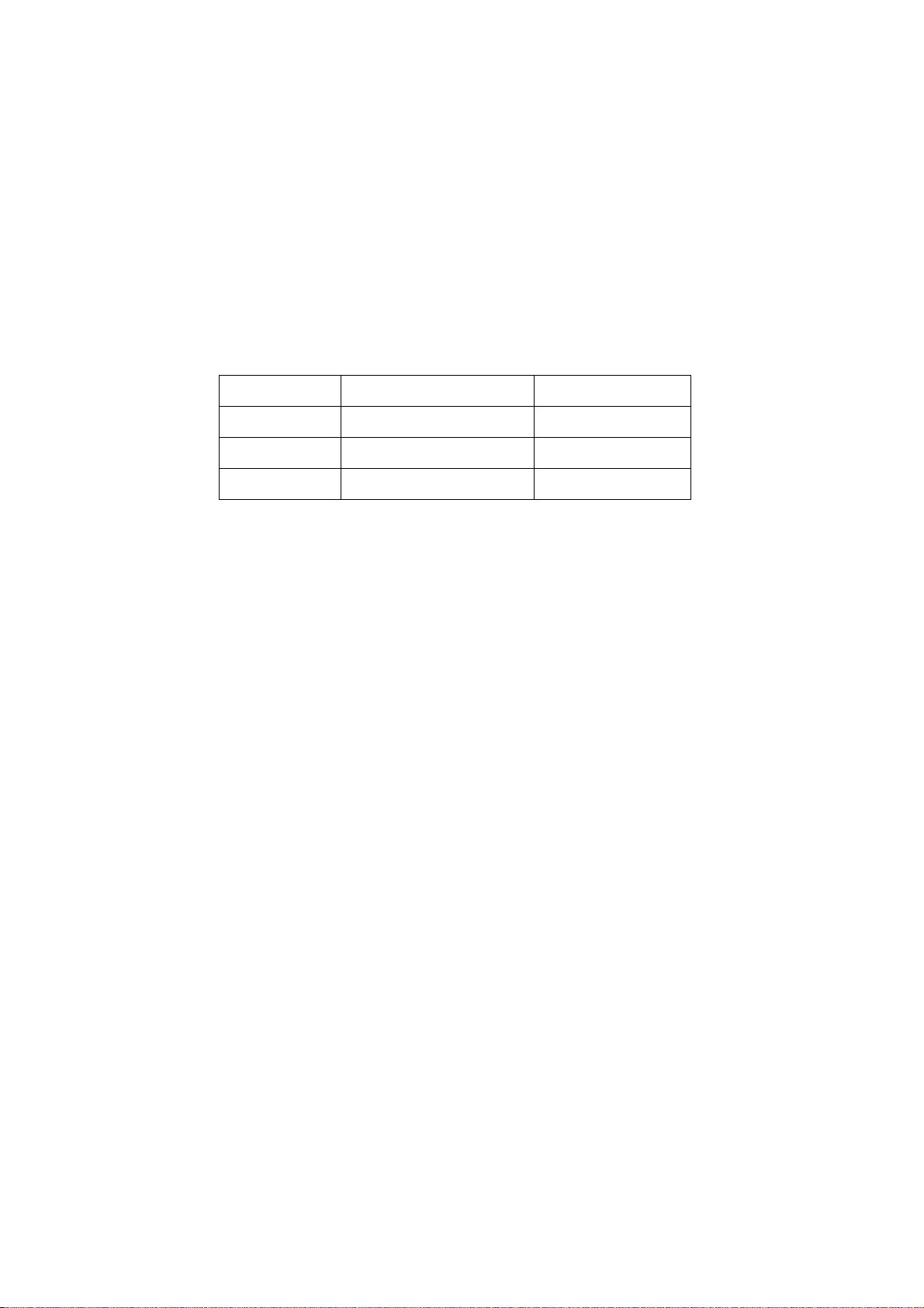
one place. The ambient conditions are tabulated as follows:
Temperature Operation range 0 ~ +50 oC
Storage range -20 ~ +60 oC
Humidity Operation range 20% ~ 85%
Storage range 10% ~ 90%
2.13 Display of a fixed picture for a long time may cause a permanent after-image on the screen,
as commonly called “ghost shadow”. The degree of the after-image varies with the maker of LCD
screen. This phenomenon doesn’t represent failure. This “ghost shadow” may remain in the
picture for a period of time (several minutes). But when operating it please avoid displaying still
picture in high brightness for a long time.
3. Installation precautions
3.1 The front panel of LCD screen is made of glass. When installing it please make sure to put it in
place.
3.2 For service or installation it’s necessary to use specified screw lest it should damage the
screen.
3.3 Be sure to take anti dust measures. Any foreign substance that happens to fall down between
the screen and the glass will affect the receiving and viewing effect
3.4 When dismantling or mounting the protective partition plate that is used for anti vibration and
insulation please take care to keep it in intactness so as to avoid hidden trouble.
3.5 Be sure to protect the cabinet from damage or scratch during service, dismantling or
mounting.
Page 5
Alignment instructions
2 Adjustment equipment
Digital multimeter
Signal generator (54200)
PC (presetting FLASH software)
VG848, VG849 (VGA, YPbPr and HDMI signal generator)
DVD player with HDMI output
White balance apparatus (CA210)
Monitor
3 Adjustment flow
3.1 Test voltage of power supply
According to wiring diagram ‘9222KC4201JL’, connect main board, power board, IR board and
key board correctly, switch on power supply, then press key ‘power’ to turn on the TV set.
a)Test voltage of socket X302 each pin in turn, please refer to voltage value as Table 3.
Table 3 Voltage of X302 each pin
X302 Pin1 2 3
3.3 V~5.0 V 1.0 V~3.3
Vol.
V
0
4、5 6、7
11.5 V~
12.5V
0
8 9 10 11 12 13
31 V~
33 V
4.7 V~5.3
V
0
4.7 V~
5.3 V
3.3 V~5.0
0
V
Page 6
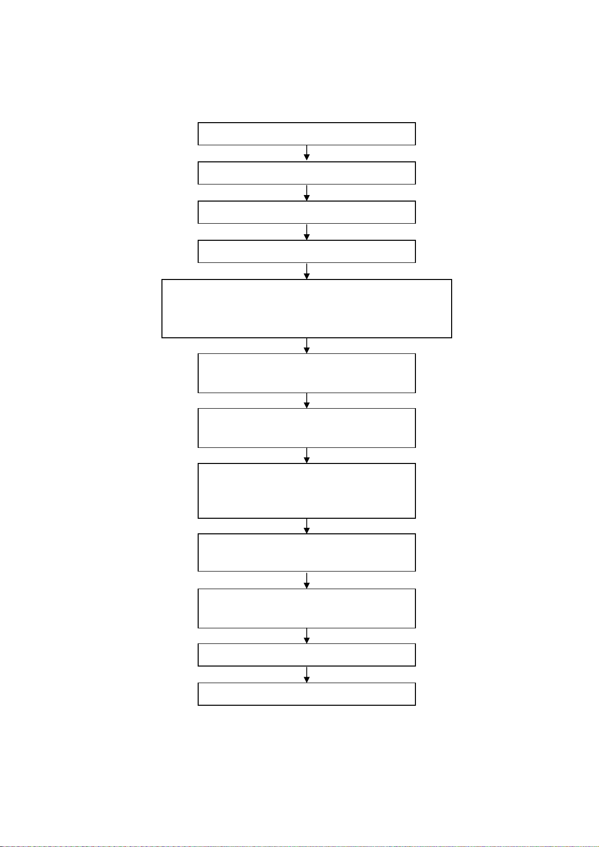
3.2 Adjustment flow chart as Fig.1
Connect to central signal source, check if each function of TV, such
as omitted program, analog parameter control, etc. is normal? Check
if output of earphones, speakers are normal?
Input AV/S-VIDEO signal, check if each function
Input HI definition signal (mode), check if each
Input VGA signal, check if display and each
function, such as analog parameters control, H/V
center, etc., are normal?
Input HDMI signal, check if display and each
function, such as analog parameters control, H/V
Insert U disk, check if functions of MP3 and JPEG
Check if FLASH has been burned
Product main board on line
General assembly and adjustment
White balance adjustment
of both channels are normal?
function of YPbPr is normal?
are normal?
Setting before leaving factory
Check accessories and packing
Fig. 1 Adjustment flow
Page 7

4 Adjustment instruction
4.1 Unit adjustment
4.1.1 According to wiring diagram ‘9242KC4201JL’ , ‘9222KC4201JL’, ‘9219KC7201JL’ ,
‘9224KC7001J’ or ‘9232KC7001JL’, connect main board, power board, key board and IR board
correctly, switch on power supply, check if display is normal?
4.1.2 Instruction of factory menu
a)First press key ‘Program source’, then press number keys “2、5、8、0” in turn to enter initial
factory menu;
b)Press keys “” and “” to move cursor to each adjustment page of initial factory menu, then
press “” to enter into its adjustment menu;
c)Press keys “” and “” to move cursor upwards or downwards within any adjustment page;
d)Press keys “” and “” to adjust any item when cursor is moved onto it;
e)Press key “Menu” to exit to initial menu from any adjustment page;
f)Press key “Exit” to exit from factory menu in any case;
g)Set item “Aging Mode” as “On” to enter into factory aging mode.
4.2 White balance adjustment
4.2.1 Before adjustment
The unit should be working for above 30 minutes to be in stabler state; Use apparatus CA210 to
adjust white balance;
For model of which dimension is bigger than 26”, only 9300K color temperature (that is “normal”)
is needed adjustment, To guarantee BBY test requirements to be met when color temperature are
12000K and 6500K, make sure that chromaticity coordinates of bright scale are (X=285±5, Y=293±8)
and chromaticity coordinates of dark scale are (X=285±8, Y=293±12);
For model of which dimension is 26” or smaller than 26”, only 8000K color temperature (that is
“normal”) is needed adjustment, To guarantee test requirements to be met when color temperature
are 9300K and 6500K, make sure that chromaticity coordinates of bright scale are X=295±5,
Y=305±8) and chromaticity coordinates of dark scale are (X=295±8, Y=305±12);
4.2.2 White balance adjustment of HDMI channel
Input 16-grey-scale signal with format of 800×600/60 Hz (VG848: Timing is 854,PAT is 921),
enter into submenu “color temperature adjustment” of factory menu;
For model of which dimension is bigger than 26”, select “normal” color temperature (that is
rd
9300K), fix item “G Offset”, adjust items “R Offset, B Offset” to set chromaticity coordinates of the 3
scale as (285±8, 293±12)and guarantee luminance within the range of 3 nit to 5 nit; fix item “G
GAIN”, adjust items “R GAIN, B GAIN” to set chromaticity coordinates of the reverse 3
rd
scale as
(285±8, 293±12); adjust items “R Offset, B Offset” and “R GAIN, B GAIN” repeatedly until
chromaticity coordinates of both scales are all (285, 293);
For model of which dimension is 26” and small than 26”, select “normal” color temperature (that is
rd
8000K), fix item “G Offset”, adjust items “R Offset, B Offset” to set chromaticity coordinates of the 3
scale as (295±8, 305±12)and guarantee luminance within the range of 3 nit to 5 nit; fix item “G
GAIN”, adjust items “R GAIN, B GAIN” to set chromaticity coordinates of the reverse 3
rd
scale as
(295±5, 305±8) ; adjust items “R Offset, B Offset” and “R GAIN, B GAIN” repeatedly until
chromaticity coordinates of both scales are all (295, 305);
Set item “ALL COLOR” as “ON” after completing adjustment.
Page 8

4.2.3 White balance adjustment of YPbPr channel
ADC calibration of SD mode: Input color-bar signal with format of 480i/60 Hz (VG848: Timing is
968,PAT is 918), enter into submenu “ADC adjustment” of factory menu and select item “AUTO
COLOR”, system will begin calibration automatically, please note whether picture and data are
abnormal clearly or not (main abnormal data phenomena are that several data are very different from
the other or about 1000 more than the other); it is failed to calibrate ADC if data are abnormal clearly,
so it is necessary to do the calibration again;
ADC calibration of HD mode: Input color-bar signal with format of 1080i/60 Hz (VG848: Timing is
972,PAT is 918), enter into submenu “ADC adjustment” of factory menu and select item “AUTO
COLOR”, system will begin calibration automatically, please note whether picture and data are
abnormal clearly or not (main abnormal data phenomena are that several data are very different from
the other or about 1000 more than the other); it is failed to calibrate ADC if data are abnormal clearly,
so it is necessary to do the calibration again;
White balance adjustment: Input 16-grey-scale signal with format of 1080i/60 Hz (VG848: Timing
is 972,PAT is 921), check if white balance is normal, if not, enter into submenu “color temperature
adjustment” of factory menu, set item “ALL COLOR” as “OFF”, please refer to step 4.2.2 to adjust
white balance for model of which dimension is 26” , bigger than 26” or smaller than 26” respectively;
Note: Item “ALL COLOR” must not be altered as “ON” again once set as “OFF”.
4.2.4 White balance adjustment of VGA channel
Auto-calibration: Input square signal with format of 800×600/60 Hz (VG848: Timing is 854,PAT is
CROSS) to do calibration automatically in order to make window filled with picture;
ADC calibration: Input monochrome signal with format of 800×600/60 Hz (VG848: Timing is 854,
PAT is 948), enter into submenu “ADC adjustment” of factory menu and select item “AUTO COLOR”,
system will begin calibration automatically, please note whether picture and data are abnormal clearly
or not (main abnormal data phenomena are that several data are very different from the other or
about 1000 more than the other); it is failed to calibrate ADC if data are abnormal clearly, so it is
necessary to do the calibration again;
White balance adjustment: Input 16-grey-scale signal with format of 800×600/60 Hz (VG848:
Timing is 854,PAT is 921), check if white balance is normal, if not, enter into submenu “color
temperature adjustment” of factory menu, set item “ALL COLOR” as “OFF”, please refer to step 4.2.2
to adjust white balance for model of which dimension is 26” , bigger than 26” or smaller than 26”
respectively;
Note: Item “ALL COLOR” must not be altered as “ON” again once set as “OFF”.
4.2.5 White balance adjustment of AV channel
Input 16-grey-scale signal with format of PAL (VG848: Timing is 969,PAT is 921), check if white
balance is normal, if not, enter into submenu “color temperature adjustment” of factory menu, set item
“ALL COLOR” as “OFF”, please refer to step 4.2.2 to adjust white balance for model of which
dimension is 26” , bigger than 26” or smaller than 26” respectively;
Note: Item “ALL COLOR” must not be altered as “ON” again once set as “OFF”.
4.2.6 Auto-white balance adjustment
4.2.6.1 ADC pre-calibration
Enter into factory menu, set “Program source” as “YPbPr”, input color-bar signal with format of
480i/60 Hz (VG848: Timing is 968,PAT is 918), enter into submenu “ADC adjustment” of factory
menu and select item “AUTO COLOR”, system will begin calibration automatically; input color-bar
signal with format of 1080i/60 Hz (VG848: Timing is 972,PAT is 918), enter into submenu “ADC
Page 9

adjustment” of factory menu and select item “AUTO COLOR”, system will begin calibration
automatically,
Press key “Menu” to be back to upper menu, set “Program source” as VGA”, input monochrome
signal with format of 800×600/60 Hz (VG848: Timing is 854,PAT is 948), enter into submenu “ADC
adjustment” of factory menu and select item “AUTO COLOR”, system will begin calibration
automatically,
4.2.6.2 White balance adjustment (models except LC-19KC72, LC-22KC72)
TV set should be working for above 30 minutes to be in stabler state before white balance
adjustment; connect CA210 to USB port of PC with data line; connect VG848 and TV to COM port of
PC or virtual COM port respectively (default connection: VG848 to COM5,TV to COM1, the
connection can be altered and saved in administrator window with password “xoceco” if necessary);
output signal of VG848 must be sent to AV1, YPbPr, VGA and HDMI1 channels of TV;
Open program file “White_Balance.exe”, load configure file “AdjustConfig.txt”, then connect
CA210, VG848 and TV respectively according to the instruction on interface.
Note: set probe to “0-CAL” before connecting CA210, press “connect CA210”, set probe back to
“MEAS” after prompt “CA-210 connection and calibration are normal !” appears on the left-down side;
BBY channel is used by CA210 for BBY models, for other models, channels except BBY are used by
CA210; please enter into administer window with password “xoceco” to alter and save apparatus
setting if it is different;
At last, press “Begin auto-white-balance-adjustment”, auto-adjustment will be completed until
prompt “Adjustment is successful” appears.
4.2.6.3 White balance adjustment (models except LC-19KC72, LC-22KC72)
TV set should be working for above 30 minutes to be in stabler state before white balance
adjustment; connect CA210 to USB port of PC with data line; connect VG848 and TV to COM port of
PC or virtual COM port respectively (default connection: VG848 to COM5,TV to COM1, the
connection can be altered and saved in administrator window with password “xoceco” if necessary);
output signal of VG848 must be sent to AV1, YPbPr, VGA and HDMI1 channels of TV;
Note: Channel shared by AV/YPBPR must be adjusted respectively.
Open program file “White_Balance.exe”, if current working progress includes AV channel, enter
into channel setting of administer window to make sure no YPBPR576i@60 but AV is chosen, or load
configure file “AdjustConfigAV.txt”; if current working progress includes YPBPR channel, enter into
channel setting of administer window to make sure no AV but YPBPR576i@60 is chosen, or load
configure file “AdjustConfigYPBPR.txt.txt”; then connect CA210, VG848 and TV respectively
according to the instruction on interface.
Note: set probe to “0-CAL” before connecting CA210, press “connect CA210”, set probe back to
“MEAS” after prompt “CA-210 connection and calibration are normal !” appears on the left-down side;
BBY channel is used by CA210 for BBY models, for other models, channels except BBY are used by
CA210; please enter into administer window with password “xoceco” to alter and save apparatus
setting if it is different;
At last, press “Begin auto-white-balance-adjustment”, auto-adjustment will be completed until
prompt “Adjustment is successful” appears.
Page 10
5 Performance check
5.1 TV port
Connect RF port to central signal source, first enter into channel menu, then auto search
programs, check if there is any omitted program ,output of speakers and picture are normal
5.2 AV/S-Video port
Input AV/S signal to corresponding terminal respectively, check if picture and sound are normal.
5.3 YPbPr/YCbCr port
Input YUV signal from signal general VG848 with YUV format listed as Table 8, check if picture
and sound are normal.
Table 8 YUV signal format
NO. Definition
1 720×480i@59.94/60 Hz 15.734 59.94/60 13.5 480i(59.94/60p)
2 720×480p@59.94/60 Hz 31.469 59.94/60 27.00 480p(59.94/60p)
3 1280×720p@59.94/60 Hz 44.96 59.94/60 74.18 720p(59.94/60p)
4 1920×1080i@59.94/60 Hz 33.75 59.94 74.25 1080i(59.94/60i)
5 1920×1080p@23.98/24 Hz 27.00 23.98/24 74.25 1080p(23.98/24p)
6 1920×1080p@59.94/60 Hz 67.50 59.94/60 148.50 1080p(59.94/60p)
H. Fre.
kHz
V. Fre.
Hz
Dot-pulse Fre.
MHz
Note
5.4 VGA port
Input VGA signal from signal general VG848 with VGA format listed as Table 9, check if picture
and sound are normal, if not, enter into menu to do auto-calibration.
Table 9 VGA signal format
NO. Definition
1 720×400@70 Hz 31.47 70.08 28.32 DOS
2 640×480@60 Hz 31.50 60.00 25.18 VESA
3 800×600@60 Hz 37.90 60.00 40.00 VESA
4 1024×768@60 Hz 48.40 60.00 65.00 VESA
1280×1024@60 Hz 63.98 60.02 108.00 VESA
5
1360×768@60 Hz 47.71 60.01 85.50 VESA
6
1920×1080@60 Hz 67.16 59.96 173.00 VESA
7
H. Fre.
kHz
V. Fre.
Hz
Dot-pulse Fre.
MHz
Note
(only for Full HD panel)
(only for 1366X768 panel)
(only for Full HD panel)
5.5 HDMI port
Input HDMIsignal from signal general VG849 with VGA format listed as Table 8&9 , check if
picture and sound are normal
5.6 USB port
Inset U disk, check if JPEG picture and MP3 music are displayed normally
5.7 AV OUT port
Check if picture and sound of AV OUT are normal
5.8 Check other functions
Check if time-on/off, sleeping time, picture/sound mode, OSD, still picture/mute and
microcrystalline-magical-picture, etc., are normal.
Page 11

6 User menu setting before leaving factory
Enter into factory menu, select item ‘Reset’, TV set will be preset automatically before leaving
factory. Be sure to do the step after completing adjustments in factory.
7 Instruction for software burning in factory as Table 10
Table 10 Instruction for software burning in factory
Loc. Part No. Part Type
N104 5272532004 W25X32VSS
Instruction for
software function
Main CPU
program
Burned before
SMT
Yes Burned software with ALL11
Method of burning
Page 12
Instruction of software upgrade
Instruction of software upgrade for KC# model:
1. Save upgrade file “flash.img” into the root directory of a U disk;
2. Insert the U disk into USB port of TV set, press key “power” until TV set is in
“standby” state, then power on TV set again;
3. Press key “program source” until menu “program source” display, then
press keys “2”, “5”, “8”, “0” by turn to enter into factory menu, please refer to
the following Fig. 1;
Fig. 1 “Program source” menu
Page 13

Fig. 2 Factory menu
4. Press keys of remote control “▲”,”▼” to select item “ISP”, press key “enter”
to begin updating progress, a prompt “Updating, Pls, Waiting…” is
displaying, wait for a while until menu display (TV set is unable to accept
other operation now), please refer to the Fig. 3;
Page 14

Fig. 3 Updating prompt
5. TV set will auto-reset after completing update, according to step1 and step
2, enter into factory menu again to confirm updating completion by
checking the time of update file.
Page 15

Working principle analysis of the unit
RF signal from antenna is sent into TUNER301 to be processed by HF-amplified and
frequency mixing, then IF signal is outputted to SWF Z301 to be IF filtered to get ideal IF
characteristics, then the signal is sent to main chip N101(RTD2674S)-27#,28# to be
amplified by inline IF amplifier and synchronous demodulated to get CVBS.
Video and audio signal from AV, S-VIDEO , YPbPr, VGA , HDMI are sent to main chip
N101(RTD2674S) directly.
Main chip N101(RTD2674S) is a special large scale IC with full functions, such as HDMI
interface process, video decoding, video switch selection, A/D and D/A transformation,
interleaved/successive scans, mode transformation, OSD and low-voltage difference
output process, etc.; furthermore, it also has functions of audio selection and process,
MCU, etc.; external video signal is processed by main chip N101(RTD2674S), then 4
pairs of difference signals and one pair of clock signals are outputted to LCD to display;
external audio signal processed by main chip N101(RTD2674S) is sent to sound amplifier
N308(TDA7266SA) to be amplified and then to speakers.
Page 16

Block Diagram
TUNER
AV
YPbPr
VGA
VGA
AUDIO
IF
CVBS
YPbPR
RGB
L/R
DDR
EM6AA160TS-
4G
RTD2674S
SPI FLASH
W25X32VSSIG-E
IC
LVDS
PANEL
SPEAKER
AMP
TDA7266SA
HP
HDMI
USB
TMDS
D+/D-
AUDIO
VIDEO
Page 17

IC block diagram
RTD2674S
Main IC
Pin List
217
U2
1
VCM_BB
2
AVDD_BB0_3.3V
3
AIN_5L/LSADC6
4
AIO_2R
5
AIO_2L
6
AIO_1R
7
AIO_1L
8
AIN_4R
9
AIN_4L
10
AIN_3R
11
AIN_3L
12
AIN_2R
13
AIN_2L
14
AIN_1R
15
AIN_1L
16
AOUT_R
17
AOUT_L
18
HPOUT_R
19
HPOUT_L
20
SCART_FSW_0
21
SCART_FSW_1
22
DAC_VDD_3.3V
23
AVOUT_1
24
AVOUT_2
25
DAC_GND
26
ADC2X_GND_3.3V
27
IF_N
28
IF_P
29
ADC2X_VDD
30
PLL_GND
31
XI N
32
XO U T
33
PLL_VDD_3.3V
34
CORE_1.2V
35
USB_AVDD_3.3V
36
HSDM
37
HSDP
38
USB_AVDD_1.2V
39
I2C0_SCL
40
I2C0_SDA
41
IO_3.3V
42
GPIO_A0/RF_AGC
43
GPIO_A1/IF_AGC
44
CORE_1.2V
45
O_FP
46
O_FN
47
O_EP
48
O_EN
49
O_DP
50
O_DN
51
O_CP
52
O_CN
53
O_BP
54
O_BN
E-PAD
213
215
216
214
VIN_A2N
AGND_BB1
(CVBS)VIN_14P
AVDD_BB1_3. 3V
212
211
(CVBS/SV-C)VIN_13P
(CVBS/SV-Y)VIN_10P
209
VIN_A1N
208
(SV-C)VIN_12P
(SV-Y)VIN_9P
206
VIN_A0N
VD_GND
VD_VDD_1.2V
(SV-C/FSC_CVBS)VIN_11P
204
205
207
210
199
196
200
201
202
203
VIN_Y1N
ADC_VDD_1.2V
(FSC_R/Y)VIN _8P
(FSC_G/Pr)VIN_7P
(FSC_B/Pb)VIN_6P
194
195
198
(Pr)VIN_5P
193
197
VIN_2N
VIN_Y0N
(Y)VIN_4P
(Pb)VIN_3P
(VGA_R)VIN_2P
RTD2674
LQFP-216
E-PAD
188
190
192
191
VIN1_N
(VGA_B)VIN_1P
189
VIN_0N
(VGA_G)VIN_0P
186
187
VSYNC
VD_VDD_3.3V
ADC_VDD_3.3V
181
185
HSYNC
180
182
183
184
APLL_GND
TMDS_1.2V
TMDS_REXT
APLL_VDD_3. 3V
P0_RX0P/HDMI _2P_0
175
177
179
178
P0_RX1P/HDMI _1P_0
P0_RX1N/HDMI_1N_0
P0_RX0N/HDMI_2N_0
176
P0_RX2P/HDMI _0P_0
P0_RX2N/HDMI_0N_0
174
173
P0_RX3P/HDMI _CLKP_0
P0_RX3N/HDMI_CLKN_0
172
P1_RX0P/HDMI _2P_1
167
169
171
168
170
P1_RX2P/HDMI _0P_1
P1_RX1P/HDMI _1P_1
P1_RX1N/HDMI_1N_1
P1_RX0N/HDMI_2N_1
163
164
165
166
TMDS_1.2V
TMDS_3.3V
HDDC0_SCL
HDDC0_SDA
P1_RX2N/HDMI_0N_1
HDDC1_SCL
P1_RX3P/HDMI _CLKP_1
P1_RX3N/HDMI_CLKN_1
HDDC1_SDA
VGA_DDC_SCL
VGA_DDC_SDA
IO_3.3V
GPIO_C8
GPIO_C6
GPIO_C5
STBY_CORE_1.2V
SPI_D O
SPI_SCK
SPI_CS_N
RESET_IN
GPIO_C4
GPIO_C3
GPIO_C2
GPIO_C1
GPIO_C0
STBY_CORE_1.2V
LSADC4/GPIO
LSADC2/GPIO
LSADC1/GPIO
LSADC0/GPIO
LSADC_REF
IO_3.3V
CORE_1. 2V
DDR_IO_2.5V
DDR_VREF
DDR_IO_2.5V
DDR_IO_2.5V
ADDR12
ADDR11
CEC
SPI_DI
DQS1
DQ_8
DQ_9
DQ_10
DQ_11
DQ_12
DQ_13
DQ_14
DQ_15
DM1
CK#
CK
CKE
ADDR9
ADDR8
ADDR7
ADDR6
ADDR5
162
161
160
159
158
157
156
155
154
153
152
151
150
149
148
147
146
145
144
143
142
141
140
139
138
137
136
135
134
133
132
131
130
129
128
127
126
125
124
123
122
121
120
119
118
117
116
115
114
113
112
111
110
109
QFP216E
O_AP55O_AN56IO_3.3V57E_FP58E_FN59E_EP60E_EN61E_DP62E_DN63E_CP64E_CN65E_BP66E_BN67E_AP68E_AN69CORE_1. 2V70TCON/GPIO_B071TCON/GPIO_B272TCON/GPIO_B373TCON/GPIO_B474TCON/GPIO_B575TCON/GPIO_B676TCON/GPIO_B777TCON/GPIO_B878IO_3.3V79TCON/GPIO_B980TCON/GPIO_B1081TCON/GPIO_B1282CORE_1. 2V83DQS084DQ_785DQ_686DDR_IO_2.5V87DQ_588DQ_489DQ_390DQ_291DQ_192DQ_093DDR_IO_2.5V94DM095WE#96CAS#97RAS#98CORE_1. 2V99BA0
100
101
BA1
102
ADDR10
103
ADDR0
ADDR1
104
105
ADDR2
ADDR3
106
107
DDR_IO_2.5V
108
ADDR4
Page 18

Main IC
RTD2674S
Table 1-1. RTD2674S Pin Assignments – Pin detail description
(I/O Legend: A = Analog, I = Input, O = Output, P = Power, G = Ground)
Pin No Pin Name Type Description Note
1
2
3
4
5
6
7
8
9
10
11
12
13
14
15
16
17
18
19
20
21
22
23
24
25
26
27
28
29
30
31
32
33
34
35
36
37
38
39
40
VCM_BB AP Analog Audio Common Voltage Reference
AVDD_BB0 AP Analog Baseband Power 3.3V
AIN_5L/LSADC6 AI Low Speed ADC input 6
AIO_2R AIO Analog Audio input/output 2 (Right Channe l)
AIO_2L AIO Analog Audio input/output 2 (Left Channel)
AIO_1R AIO Analog Audio input/output 1 (Right Channe l)
AIO_1L AIO Analog Audio input/output 1 (Left Channel)
AIN_4R AI Analog Audio input 4 (Right Channel)
AIN_4L AI Analog Audio input 4 (Left Channel)
AIN_3R AI Analog Audio input 3 (Right Channel)
AIN_3L AI Analog Audio input 3 (Left Channel)
AIN_2R AI Analog Audio input 2 (Right Channel)
AIN_2L AI Analog Audio input 2 (Left Channel)
AIN_1R AI Analog Audio input 1 (Right Channel)
AIN_1L AI Analog Audio input 1 (Left Channel)
AOUT_R AO Analog Baseband Audio Out (Right Channel)
AOUT_L AO Analog Baseband Audio Out (Left Channel)
HPOUT_R AO Head Phone DAC output (Right Channel)
HPOUT_L AO Head Phone DAC output (Left Channel)
Scart_FSW_0 AIO SCART RGB Fast Switch Input 0
Scart_FSW_1 AIO SCART RGB Fast Switch Input 1
DAC_VDD_0 AP Video DAC Power 3.3V
AVOUT_1 AP CVBS DAC output1
AVOUT_2 AP CVBS DAC output2
DAC_GND_0 AP Video DAC GND
ADC2X_GND_1 AP IFADC GND
IF_N AP IF demod Negative input
IF_P AP IF demod Postive input
ADC2X_VDD_0 AP IFADC power 3.3V
PLL_GND_1 AP XTAL PLL GND
XIN AP 27MHz Crystal Input
XOUT AP 27MHz Crystal Output
PLL_VDD_0 AP XTAL PLL power 3.3V
Core_1.2V DP Core Power 1.2V
AVDD_1 AP USB Power 3.3V
HSDM_1 AP USB HOST0 Data Negative
HSDP_1 AP USB HOST0 Data Postive
LV_USB_1 AP USB Power 1.2V
I2C0_SCL DIO Tuner I2C clock
I2C0_SDA DIO Tuner I2C data
Connect 1uF to GND
Analog 3.3V
Analog 3.3V
Analog 3.3V
Analog 3.3V
Digital 1.2V, Power Down@
Power saving
Analog 3.3V
Analog 1.2V
5V tolerance even when
power-off
5V tolerance even when
power-off
Page 19

Main IC
RTD2674S
41
42
43
44
45
46
47
48
49
50
51
52
53
54
55
56
57
58
59
60
61
62
63
64
65
66
67
68
69
70
71
72
73
74
75
76
77
78
79
VCC3_0 P PAD I/O Power 3.3V
GPIO_A0 DIO GPIO_A0
GPIO_A1 DIO GPIO_A1
Core_1.2V P Core Power 1.2V
B_FP AO LVDS_Port_B_F_Pair_P
B_FN AO LVDS_Port_B_F_Pair_N
B_EP AO LVDS_Port_B_E_Pair_P
B_EN AO LVDS_Port_B_E_Pair_N
B_DP AO LVDS_Port_B_D_Pair_P
B_DN AO LVDS_Port_B_D_Pair_N
B_CP AO LVDS_Port_B_C_Pair_P
B_CN AO LVDS_Port_B_C_Pair_N
B_BP AO LVDS_Port_B_B_Pair_P
B_BN AO LVDS_Port_B_B_Pair_N
B_AP AO LVDS_Port_B_A_Pair_P
B_AN AO LVDS_Port_B_A_Pair_N
LVDSV P LVDS Power 3.3V
A_FP AO LVDS_Port_A_F_Pair_P
A_FN AO LVDS_Port_A_F_Pair_N
A_EP AO LVDS_Port_A_E_Pair_P
A_EN AO LVDS_Port_A_E_Pair_N
A_DP AO LVDS_Port_A_D_Pair_P
A_DN AO LVDS_Port_A_D_Pair_N
A_CP AO LVDS_Port_A_C_Pair_P
A_CN AO LVDS_Port_A_C_Pair_N
A_BP AO LVDS_Port_A_B_Pair_P
A_BN AO LVDS_Port_A_B_Pair_N
A_AP AO LVDS_Port_A_A_Pair_P
A_AN AO LVDS_Port_A_A_Pair_N
Core_1.2V P Core Power 1.2V
GPIO_B0 DIO GPIO_B0
GPIO_B2 DIO GPIO_B2
GPIO_B3 DIO GPIO_B3
GPIO_B4 DIO GPIO_B4
GPIO_B5 DIO GPIO_B5
GPIO_B6 DIO GPIO_B6
GPIO_B7 DIO GPIO_B7
GPIO_B8 DIO GPIO_B8
VCC3_2 P PAD I/O Power 3.3V
Digital I/O 3.3V
5V tolerance even when
power-off
5V tolerance even when
power-off
Digital 1.2V, Power Down@
Power saving
Digital 1.2V, Power Down@
Power saving
5V tolerance even when
power-off
5V tolerance even when
power-off
5V tolerance even when
power-off
5V tolerance even when
power-off
5V tolerance even when
power-off
5V tolerance even when
power-off
5V tolerance even when
power-off
5V tolerance even when
power-off
Page 20

Main IC
80
81
82
83
84
85
86
87
88
89
90
91
92
93
94
95
96
97
98
99
100
101
102
103
104
105
106
107
108
109
110
111
112
113
114
115
116
117
118
119
120
121
122
RTD2674S
GPIO_B9 DIO GPIO_B9
GPIO_B10 DIO GPIO_B10
GPIO_B12 DIO GPIO_B12
Core_1.2V P Core Power 1.2V
DQS0 DO DDR_DQS0
DQ_7 DIO DDR_Data7
DQ_6 DIO DDR_Data6
SVCC25 P DDR I/O Power 2.5V
DQ_5 DIO DDR_Data5
DQ_4 DIO DDR_Data4
DQ_3 DIO DDR_Data3
DQ_2 DIO DDR_Data2
DQ_1 DIO DDR_Data1
DQ_0 DIO DDR_Data0
SVCC25 P DDR I/O Power 2.5V
DM0 DO DDR_Data_Mask0
WE# DO DDR Write Enable (Low Enable)
CAS# DO DDR CAS (Low Enable)
RAS# DO DDR RAS (Low Enable)
Core_1.2V P Core Power 1.2V
BA0 DO DDR Bank Address0
BA1 DO DDR Bank Address1
ADDR10 DO DDR Address10
ADDR0 DO DDR Address0
ADDR1 DO DDR Address1
ADDR2 DO DDR Address2
ADDR3 DO DDR Address3
SVCC25 P DDR I/O Power 2.5V
ADDR4 DO DDR Address4
ADDR5 DO DDR Address5
ADDR6 DO DDR Address6
ADDR7 DO DDR Address7
ADDR8 DO DDR Address8
ADDR9 DO DDR Address9
ADDR11 DO DDR Address11
ADDR12 DO DDR Address12
CKE DO DDR Clock Enable
SVCC25 P DDR I/O Power 2.5V
CK DO DDR Clock Differential(+)
CK# DO DDR Clock Differential(-)
DM1 DO DDR Data Mask1
SVCC25 P DDR I/O Power 2.5V
VREF AI DDR Reference Voltage Input
5V tolerance even when
power-off
5V tolerance even when
power-off
5V tolerance even when
power-off
Digital 1.2V, Power Down@
Power saving
Digital 1.2V, Power Down@
Power saving
1.25V Ref input
Page 21

Main IC
RTD2674S
123
124
125
126
127
128
129
130
131
132
133
134
135
136
137
138
139
140
141
142
143
144
145
146
147
148
149
150
151
152
153
154
155
156
157
158
159
DQ_15 DIO DDR_Data15
DQ_14 DIO DDR_Data14
DQ_13 DIO DDR_Data13
DQ_12 DIO DDR_Data12
DQ_11 DIO DDR_Data11
DQ_10 DIO DDR_Data10
SVCC25 P DDR I/O Power 2.5V
DQ_9 DIO DDR_Data9
DQ_8 DIO DDR_Data8
DQS1 DO DDR_DQS1
Core_1.2V P Core Power 1.2V
V33_IO P PAD I/O Power 3.3V
lsadc_ref AI LSADC reference
lsadc0 AI LSADC0
lsadc1 AI LSADC1
lsadc2 AI LSADC2
lsadc4 AI LSADC4
STBY_Core_1.2V P Standby ON Core Power 1.2V
GPIO_C0 DIO GPIO_C0
GPIO_C1 DIO GPIO_C1
GPIO_C2 DIO GPIO_C2
GPIO_C3 DIO GPIO_C3
GPIO_C4 DIO GPIO_C4
RSTI DI Chip Reset Input
SPI_CSn DO SPI Flash CS Output
SPI_SCLK DO SPI Flash Clock Output
SPI_SDO DO SPI Flash Data Output
SPI_SDI DI SPI Flash Data Input
STBY_Core_1.2V P Standby ON Core Power 1.2V
GPIO_C5 DIO GPIO_C5
GPIO_C6 DIO GPIO_C6
GPIO_C8 DIO GPIO_C8
VCC3_4 P PAD I/O Power 3.3V
VDDC_SDA DIO VGA DDC Data
VDDC_SCL DIO VGA DDC Clock
HDDC1_SDA DIO HDMI DDC Data 1
HDDC1_SCL DIO HDMI DDC Clock 1
Digital 1.2V, Power Down@
Power saving
Connect 10K to GND
Digital 1.2V, Always On@
Power saving
5V tolerance even when
power-off
5V tolerance even when
power-off
5V tolerance even when
power-off
5V tolerance even when
power-off
5V tolerance even when
power-off
Low Active
Digital 1.2V, Always On@
Power saving
5V tolerance even when
power-off
5V tolerance even when
power-off
5V tolerance even when
power-off
5V tolerance even when
power-off
5V tolerance even when
power-off
5V tolerance even when
power-off
5V tolerance even when
power-off
Page 22

Main IC
160
161
162
163
164
165
166
167
168
169
170
171
172
173
174
175
176
177
178
179
180
181
182
183
184
185
186
187
188
189
190
191
192
193
194
195
196
197
198
199
200
201
202
203
RTD2674S
HDDC0_SDA DIO HDMI DDC Data 0
HDDC0_SCL DIO HDMI DDC Clock 0
CEC DIO HDMI CEC function
RX_V12 AP HDMI GDI Power 1.2V
RX_V33 AP HDMI GDI Power 3.3V
HDMI_1_CLKN AI HDMI_RX_Port1_CLK_Pair_Negative
HDMI_1_CLKP AI HDMI_RX_Port1_CLK_Pair_Positive
HDMI_1_0N AI HDMI_RX_Port1_Pair0_Negative
HDMI_1_0P AI HDMI_RX_Port1_Pair0_Positive
HDMI_1_1N AI HDMI_RX_Port1_Pair1_Negative
HDMI_1_1P AI HDMI_RX_Port1_Pair1_Positive
HDMI_1_2N AI HDMI_RX_Port1_Pair2_Negative
HDMI_1_2P AI HDMI_RX_Port1_Pair2_Positive
HDMI_0_CLKN AI HDMI_RX_Port0_CLK_Pair_Negative
HDMI_0_CLKP AI HDMI_RX_Port0_CLK_Pair_Positive
HDMI_0_0N AI HDMI_RX_Port0_Pair0_Negative
HDMI_0_0P AI HDMI_RX_Port0_Pair0_Positive
HDMI_0_1N AI HDMI_RX_Port0_Pair1_Negative
HDMI_0_1P AI HDMI_RX_Port0_Pair1_Positive
HDMI_0_2N AI HDMI_RX_Port0_Pair2_Negative
HDMI_0_2P AI HDMI_RX_Port0_Pair2_Positive
TMDS_REXT AI TMDS External Resistor Input
RX_V12 AP HDMI GDI Power 1.2V
APLL_VDD AP APLL Power 3.3V
APLL_GND AP APLL GND
HSYNC AI Hsync input
VSYNC AI Vsync input
ADC_VDD33 AP ADC Power 3.3V
ADC_VDC_VDD33 AP ADC Power 3.3V
VIN_0P AI ADC Blue Input 1 Positive
VIN_BN AI ADC Blue Input 1 Negative
VIN_1P AI ADC Green Input 1 Positive
VIN_GN AI ADC Green Input 1 Negative
VIN_2P AI ADC Red Input 1 Positive
VIN_RN AI ADC Red Input 1 Negative
VIN_3P AI YPbPr Blue Input
VIN_Y0N AI Common GND for YPbPr
VIN_4P AI YPbPr Green Input
VIN_5P AI YPbPr Red Input
VIN_6P AI YPbPr Blue Input/Scart Blue
VIN_Y1N AI Common GND for YPbPr/Scart
VIN_7P AI YPbPr Green Input/Scart Green
VIN_8P AI YPbPr Red Input/Scart Red/Scart C
ADC_VDD12 AP ADC Power 1.2V
5V tolerance even when
power-off
5V tolerance even when
power-off
5V tolerance even when
power-off
Connect 6. 2K to GND
Page 23

Main IC
RTD2674S
204
205
206
207
208
209
210
211
212
213
214
215
216 AGND_BB1 AP Analog Baseband GND
Note
ADC_VDC_VDD12 AP ADC Power 1.2V
ADC_GND_OFF AP ADC GND
VIN_11P AI S-Video C/Scart C Input
VIN_A0N AI Common GND for Scart/SV
VIN_9P AI S-Video Y/Scart Y Input
VIN_12P AI S-Video C Input
VIN_A1N AI Common GND for SV
VIN_10P AI S-Video Y Input
VIN_13P AI CVBS Input
VIN_A2N AI Common GND for CVBS
VIN_14P AI CVBS Input
AVDD_BB1 AP Analog Baseband Power 3.3V
1. AP : Analog Power/Ground
2. AI : Analog Input
3. AO : Analog Output
4. AIO : Analog Input/Output
5. DP : Digital Power/Ground
6. I : Digital Input
7. O: Digital Output
8. IO : Digital Input/Output
Page 24

TDA7266SA Sound Power Amplifier
Page 25

Wiring diagram
Page 26

Troubleshooting flow
1. No raster
Page 27

2. No picture, but sound is normal
Page 28

3. No sound, but picture is normal.
Page 29

Page 30

Page 31

Page 32

Page 33

APPENDIX-B: Exploded view (LCD-22R35FHD)
Page 34

PART LIST OF EXPLODED VIEW
REF.No. DESCRIPION
1 Front cabinet assembly
2
3 Main frame
4
5
6
7
8
9 Interface baffle (down)
10 Power cord clip
11 Interface baffle
12 Key board assembly
13
14
15
Display panel
Main board assembly
Power / backlight board assembly
Back cover assembly
Standing pole assembly
Pedestal assembly
Speaker assembly
IR assembly
Light-guided pole
Note: design and specification are subject to change without notice.
Page 35

PART LIST
LCD-22R35FHD ver.1.0
REF.No. PARTS No. DESCRIPION Q'TY REMARK
1
2
3
4
5
6
7
8
9
10
11
12
13
14
15
16
17 XI5944038790
XI662242005D
XI5203228203
XI574022801D
XI6KC03101B0
XI6KH0022010
XI672242N020
XI6156090800
XI6151201010
XI5810M6870A
XI572011201C
XI5810H68610
XI6KC0250510
XI6170847000
XI6KC0310910
XI5700315010
XI6010J03505
Front cabinet assembly 1
Display panel
Main frame 1
Main board assembly
Power / backlight board assembly
Back cover assembly
Standing pole assembly
Pedestal assembly
Interface baffle (down) 1
Power cord clip 1
Interface baffle 1
Key board assembly 1
Speaker assembly
IR assembly
Light-guided pole
Remote control
User manual
1 CLAA215FA01 V2
1
1
1
1
1
1
1
1
1
1
Only the parts in above list are used for repairing.
Other parts except the above parts can't be supplied.
Page 36

Appendix: Installing the Stand
If the stand is provided, please read these instructions thoroughly before attempting this installation.
You must install your TV into the stand in order for it to stand upright on a cabinet or other flat surface. If you intend
to mount your TV on a wall or other vertical surface, you must remove the stand column.
Cautions:
Make sure that you handle your TV very carefully when attempting assembly or removal of the stand. If you are not
sure of your ability to do this, or of your ability to use the tools necessary to complete this job, refer to a professional
installer or service personnel. The manufacturer is not responsible for any damages or injuries that occur due to
mishandling or improper assembly.
The speaker is not intended to support the weight of your TV. Do not move or handle your TV by the speaker. This
can cause damage to your TV that is not covered by the manufacturer's warranty.
Before attempting assembly or removal of the stand, unplug the AC power cord.
Installing the stand
Push downward s
Stand groove
Stand column
Stand
Adjusting the viewing angle
forward
Stand
Stand
backward
To install the stand:
Place the stand on the table, hold the display upright and aim the
bottom stand column toward the stand groove, then carefully push
the display downwards, fully insert the column into the stand until the
lock snaps. Now the stand is assembled.
To adjust the viewing angle:
Tilt the screen forward 5 or backward 10 .
Caution: When adjusting the viewing angle, be careful not to tip over
your TV.
o o
5°
Detaching the Stand
10°
To detach the stand:
1.Place carefully the display on its front side with a soft cushion
90
below, shake the stand forward or backward to adjust angle
between the stand and the display, let the angle ≤ 90°.
Page 37

Appendix: Installing the Stand (Continued)
Pull out the stan d
Pre ss together
and push inside
Tabs
Removing the Stand Column
2.Press the two tabs together and push inside properly, and pull out
the stand at the same time to detach the stand.
To remove the stand column:
If wall mounting, please detach the stand column.
Place carefully the display on its front side with a soft cushion below,
loosen and remove 4 pcs screws, detach the stand column.
Stand Column
4 pcs screws
NOTE:
!The appearance of this product in these illustrations may differ from your actual product, and is for
comparative purposes only.
Page 38

WALL MOUNTING INSTRUCTIONS
Safety Precautions:
1. Be sure to ask an authorized service personnel to carry out setup.
2. Thoroughly read this instruction before setup and follow the steps below precisely.
3.The wall to be mounted should be made from solid materials. Only use accessories supplied by the manufacturer.
4.Very carefully handle the unit during setup. We are not liable for any damage or injury caused by mishandling or improper installation.
5.Be sure to place the unit on a stable and soft platform which is strong enough to support the unit.
6.Do not uplift the speaker when moving the display. The appearance of the unit may different from the actual ones.
7.Design and specifications are subject to change without notice.
8. Retain these instructions for future reference.
Note: All the wall mounting parts are optional and may be unavailable in your model.
Below we will show you how to mount the Display on the wall using our company’s wall mounting components.
11
Take out these parts from the box.
Wall Mounting
Component
(including bracket
and connector)
Expansion Bolt
Wood Screw
M4 Screw
Fig. 1
Fully insert the two insertions on the wall mounting connector into the
44
locating grooves on the wall mounting bracket from top to bottom end.
22
Screw 4pcs expansion bolts to fix
the wall mounting bracket on the
wall.
Wall
Wall Mounting Bracket
Fig. 2a
If your wall is a wooden structure, please
fix the wall mounting bracket on the wall
with 8 pcs wood screws.
Wall
Wall Mounting Bracket
Fig. 2b
55
Use screwdriver to revolve the Clasper to the Positioner
following the direction of the arrow.
33
Use the 4pcs M4 screws to fix the wall
mounting connector to the rear of the
display unit.
Wall Mounting Connector
Fig. 3
Clasper
Positioner
Fig. 4
Fig. 5
Page 39

February 2011
 Loading...