


Overview
The LC9997M is a 1/5-inch optical size frame transfer
CCD solid-state image sensor.
Features
• Effective pixels [total pixels]: 508 × 246 [532 × 250] (H
× V)
• Number of optical black pixels:
Horizontal:2 in front, 22 in back
Vertical: 2.5 above, 1.5 below
• Dummy bits: Horizontal: 4 pixels
• Horizontal resolution: 330 TV lines
• Small form factor supports compact application products
• 20-pin half-pitch transparent DIP package
• Horizontal shift register operates at 5 V.
• Supports variable-speed electronic shutter operation.
Device Structure
• 1/5-inch optical size frame transfer CCD image sensor
• Unit cell size: 5.8 µm ×9.0 µm (H × V)
• Chip size: 4.18 mm × 5.10 mm (H × V)
• Parallel gate CCD sensor
• Built-in high-sensitivity output amplifier
• Cy-G-Ye-W mosaic complementary color filters
Package Dimensions
unit: mm
3217
53098RM (OT) No. 5783-1/11
Preliminary
[LC9997M]
SANYO Electric Co.,Ltd. Semiconductor Bussiness Headquarters
TOKYO OFFICE Tokyo Bldg., 1-10, 1 Chome, Ueno, Taito-ku, TOKYO, 110-8534 JAPAN
1/5-Inch Frame Transfer CCD
NTSC Color Image Sensor
LC9997M
Ordering number : EN*5783
Parameter Symbol Conditions Ratings Unit
Supply voltage V
DD
VPW= 0 V –0.3 to +18 V
Load gate voltage V
GG
VPW= 0 V –0.3 to +5 V
N substrate - p-well voltage NSUB–VPW –0.3 to +50 V
N substrate - image and storage area voltage NSUB–
φ
1 to φ4, φS1 to φS4 –0.3 to +55 V
Horizontal clock pin,
φ
R: VPW= 0 V –0.3 to +18 V
Pin voltage Other clock pins: V
PW
= 0 V –15 to +18 V
Other pins: V
PW
= 0 V –0.3 to +10 V
Operating temperature Topr –10 to +60 °C
Storage temperature Tstg –30 to +80 °C
Specifications
Absolute Maximum Ratings at Ta = 25°C
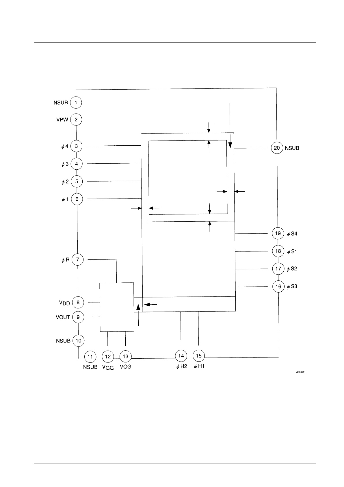
Block Diagram
No. 5783-2/11
LC9997M
Optical black area
1.5 pixels
Imaging area
2 pixels
22 pixels
2.5 pixels
Storage area
4 dummy bits
Output block
Horizontal shift register (CCD)
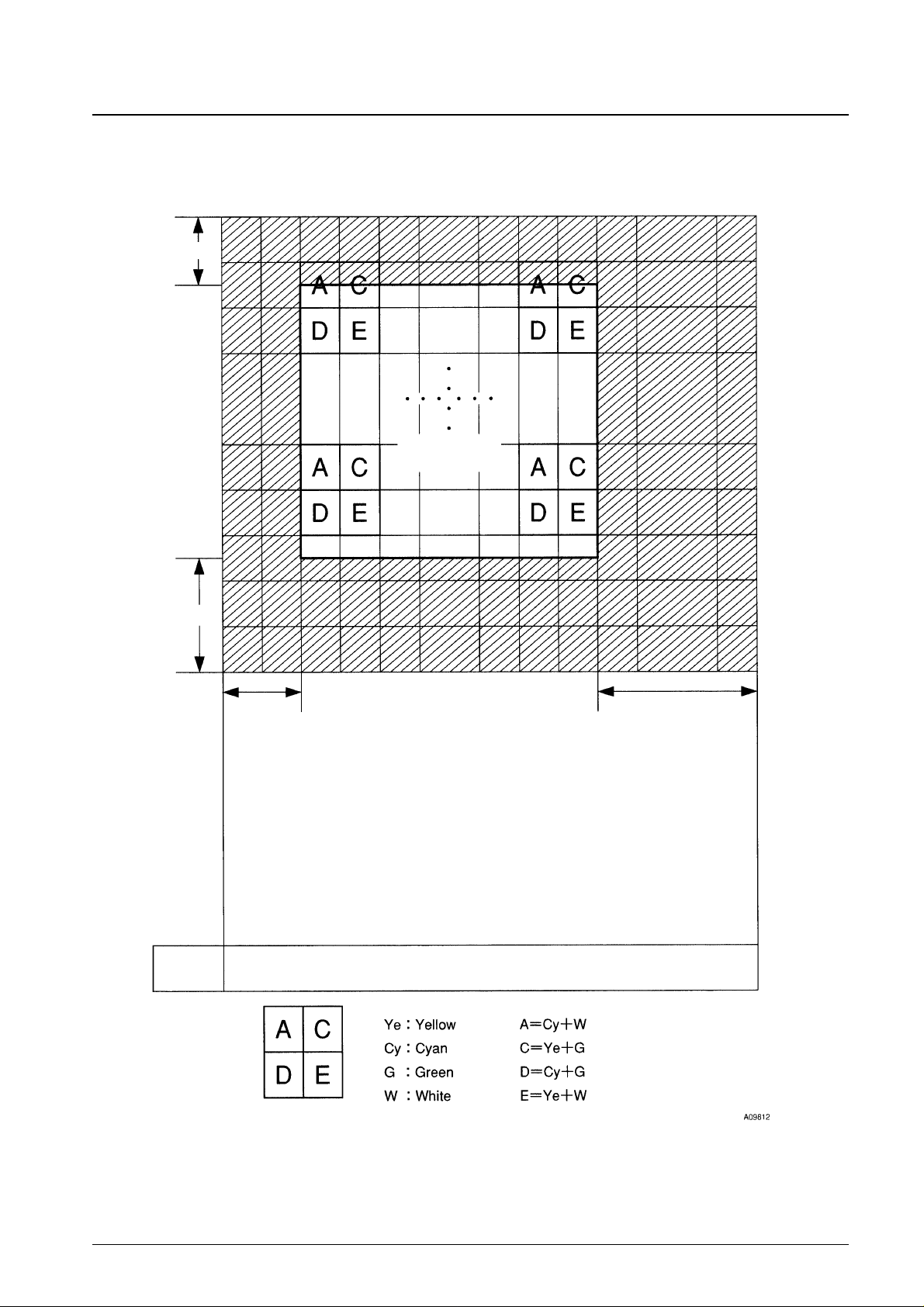
Pixel Arrangement
No. 5783-3/11
LC9997M
1.5 pixels
2.5 pixels
2 pixels
22 pixels
Imaging area
Storage area
Horizontal shift register
Output
amplifier
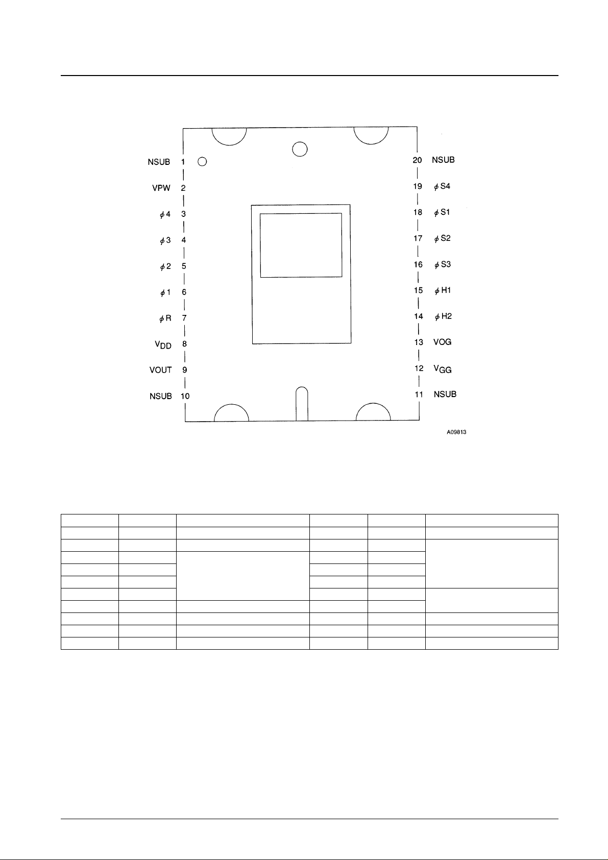
Pin Assignment
No. 5783-4/11
LC9997M
Pin Functions
Pin No. Symbol Function Pin No. Symbol Function
1 NSUB N substrate 20 NSUB N substrate
2 WPW P-well 19 φ S4
3 φ 4 18 φ S1
Storage area clocks
4 φ 3
Imaging area clock
17 φ S2
5 φ 2 16 φ S3
6 φ 1 15 φ H1
Horizontal block clocks
7 φR Reset gate 14 φ H2
8 V
DD
Supply voltage 13 V
OG
CCD output gate
9 V
OUT
CCD output 12 V
GG
Load gate
10 NSUB N substrate 11 NSUB N substrate
 Loading...