

Page 1
Ordering number : ENN*6282
O1899RM (OT) No. 6282-1/5
Overview
The LC99350 is a low-cost frame transfer CCD (chargecoupled device) solid-state imaging element that features
1.1M pixels in a 2/5-inch optical size. It supports both
progressive scan readout of all 1296 × 846 pixels as well
as a real-time monitor mode with data compressed by 1/3.
Applications
PC cameras, TV telephones, image input units, and digital
still cameras
Features
• Progressive scan readout
• Real-time compressed-data monitor mode
• Variable speed electronic shutter
• Horizontal dual readout adopted (Since the even and odd
pixels on a single horizontal line are read out in two
operations, a line memory is required for signal
processing.)
Image Sensor Element Structure
• Effective pixels [Total pixels]: 1296 × 864 [1392 × 888]
(H×V)
• Number of optical blacks:
Horizontal: 84 at the front, 12 at the rear
Vertical direction: 12 at the top, 12 at the bottom
• Dummy bits: Horizontal: 6 pixels
• Unit cell size: 4.5 µm × 4.5 µm (H×V)
• Primary color mosaic filters (RGB)
• Parallel gate CCD sensor
• Consists of a 1392 × 888-pixel imaging block and a
1392 × 296-pixel storage block
• Three-phase drive used for the imaging and storage
blocks, and 2-phase drive for the horizontal transfer
block
• Built-in high-sensitivity output amplifier
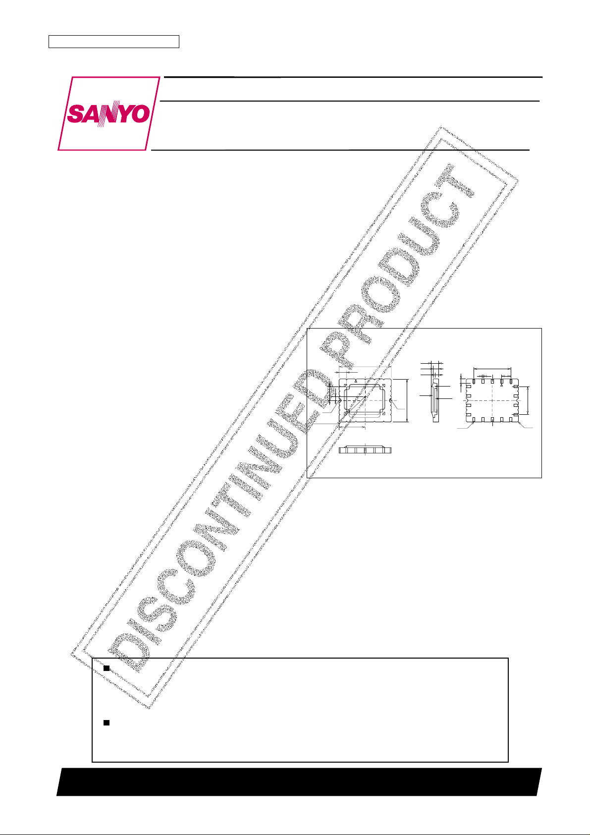
14.3
2.04
1.49
1.075
7.15
10.16
3.7
1.0
0.7
2.54
11.8
1.2
7.62
R0.3
R0.5
R0.6
R0.25
2.0
Resin
Optical Center
Glass
Sensor
Preliminary
[LC99350]
LC99350
SANYO Electric Co.,Ltd. Semiconductor Company
TOKYO OFFICE Tokyo Bldg., 1-10, 1 Chome, Ueno, Taito-ku, TOKYO, 110-8534 JAPAN
2/5-Inch Frame Transfer CCD
1.1M Pixel Color Image Sensor
Any and all SANYO products described or contained herein do not have specifications that can handle
applications that require extremely high levels of reliability, such as life-support systems, aircraft’s
control systems, or other applications whose failure can be reasonably expected to result in serious
physical and/or material damage. Consult with your SANYO representative nearest you before using
any SANYO products described or contained herein in such applications.
SANYO assumes no responsibility for equipment failures that result from using products at values that
exceed, even momentarily, rated values (such as maximum ratings, operating condition ranges, or other
parameters) listed in products specifications of any and all SANYO products described or contained
herein.
Package Dimensions
unit: mm
3250
Page 2
No. 6282-2/5
LC99350
Parameter Symbol Conditions Ratings Unit
Supply voltage V
DD
, VRDVPW= 0 V –0.3 to +15 V
Load gate voltage V
GG
VPW= 0 V –0.3 to +3 V
N substrate p-well voltage NSUB–PW: V
PW
= 0 V –0.3 to +35 V
N substrate imaging and storage block voltage NSUB–PI1 to PI3, PS1 to PS3: V
PW
= 0 V –0.3 to +35 V
Horizontal block clock and reset gate voltage Horizontal clock pin and PR: V
PW
= 0 –0.3 to +15 V
Clock voltage Clock pins other that the above: V
PW
= 0 –15 to +15 V
Pin voltage Pins other than the above –0.3 to +10 V
Operating temperature Topr –10 to +60 °C
Storage temperature Tstg –30 to +80 °C
Specifications
Absolute Maximum Ratings at Ta = 25°C
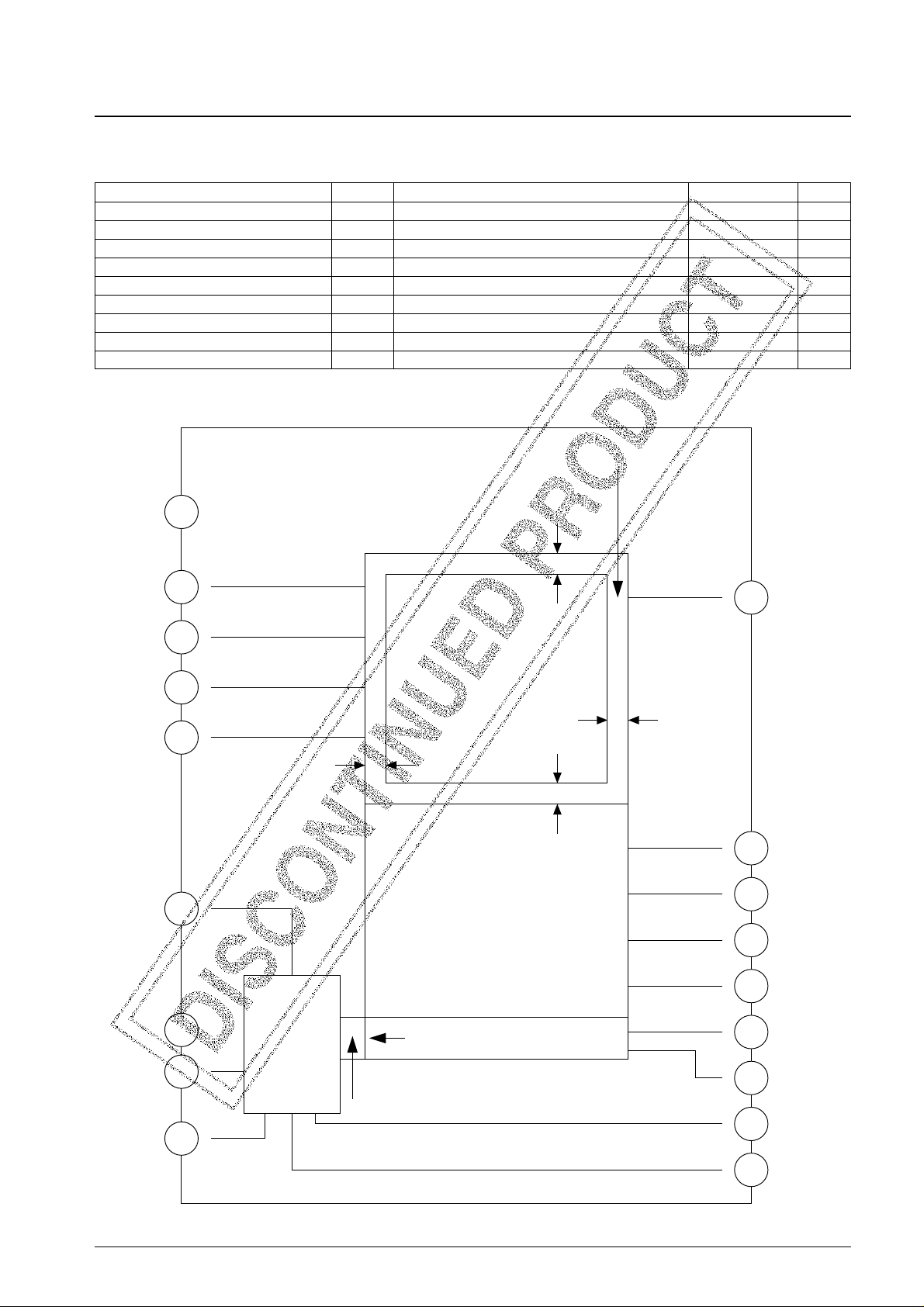
Block diagram
1VPW
2PI3
3PI2
4PI1
5TG1
6PR
7VRD
8V
DD
9VOUT
18
NSUB
17
PS1
16
PS2
15 PS3
14 TG2
13 PH1
12 PH2
11 VOG
10 V
GG
Imaging block
Storage block
Output
block
84 pixels
Horizontal shift register (CCD)
6 dummy bits
12 pixels
12 pixels
12 pixels
Optical black area
A12670
Page 3

Pixel Arrangement
No. 6282-3/5
LC99350
1234
1293
1294
1295
1296
GBRGGBR
G
GBRGGBR
G
GBRGGBR
G
GBRGGBR
G
Imaging area
Effective pixels:
1296 × 864 (H×V)
Storage block
Total pixels:
1392 × 296 (H×V)
Horizontal shift register (1392 pixels)
Dummy bits
(6 pixels)
(84 pixels)
Optical black
area
(12 pixels)
Optical black area
Optical black
area
(12 pixels)
(12 pixels)
Optical black area
A12671
Page 4

Pin Arrangement
No. 6282-4/5
LC99350
PI2
PI1
TG1
PR
VRD
PS3
TG2
PH1
PH2
V
DD
VOUT V
GG
VOG
PI3
VPW NSUB PS1 PS2
A12672
Pin Functions
Pin No. Symbol Function Pin No. Symbol Function
1 VPW P-well 18 NSUB N substrate
2 PI3 17 PS1
3 PI2 Imaging block clock 16 PS2 Storage block clock
4 PI1 15 PS3
5 TG1 Transfer gate 14 TG2 Transfer gate
6 PR Reset gate 13 PH1
Horizontal block clock
7 VRD Reset drain 12 PH2
8V
DD
Supply voltage 11 V
OG
CCD output gate
9V
OUT
CCD output 10 V
GG
Load gate
Page 5

PS No. 6282-5/5
LC99350
This catalog provides information as of October, 1999. Specifications and information herein are subject
to change without notice.
Specifications of any and all SANYO products described or contained herein stipulate the performance,
characteristics, and functions of the described products in the independent state, and are not guarantees
of the performance, characteristics, and functions of the described products as mounted in the customer’s
products or equipment. To verify symptoms and states that cannot be evaluated in an independent device,
the customer should always evaluate and test devices mounted in the customer’s products or equipment.
SANYO Electric Co., Ltd. strives to supply high-quality high-reliability products. However, any and all
semiconductor products fail with some probability. It is possible that these probabilistic failures could
give rise to accidents or events that could endanger human lives, that could give rise to smoke or fire,
or that could cause damage to other property. When designing equipment, adopt safety measures so
that these kinds of accidents or events cannot occur. Such measures include but are not limited to protective
circuits and error prevention circuits for safe design, redundant design, and structural design.
In the event that any or all SANYO products (including technical data, services) described or contained
herein are controlled under any of applicable local export control laws and regulations, such products must
not be exported without obtaining the export license from the authorities concerned in accordance with the
above law.
No part of this publication may be reproduced or transmitted in any form or by any means, electronic or
mechanical, including photocopying and recording, or any information storage or retrieval system,
or otherwise, without the prior written permission of SANYO Electric Co., Ltd.
Any and all information described or contained herein are subject to change without notice due to
product/technology improvement, etc. When designing equipment, refer to the “Delivery Specification”
for the SANYO product that you intend to use.
Information (including circuit diagrams and circuit parameters) herein is for example only; it is not
guaranteed for volume production. SANYO believes information herein is accurate and reliable, but
no guarantees are made or implied regarding its use or any infringements of intellectual property rights
or other rights of third parties.
 Loading...