

Overview
The LC99063-LF2 is a color video signal processor for
use with the LC9997M/FL.
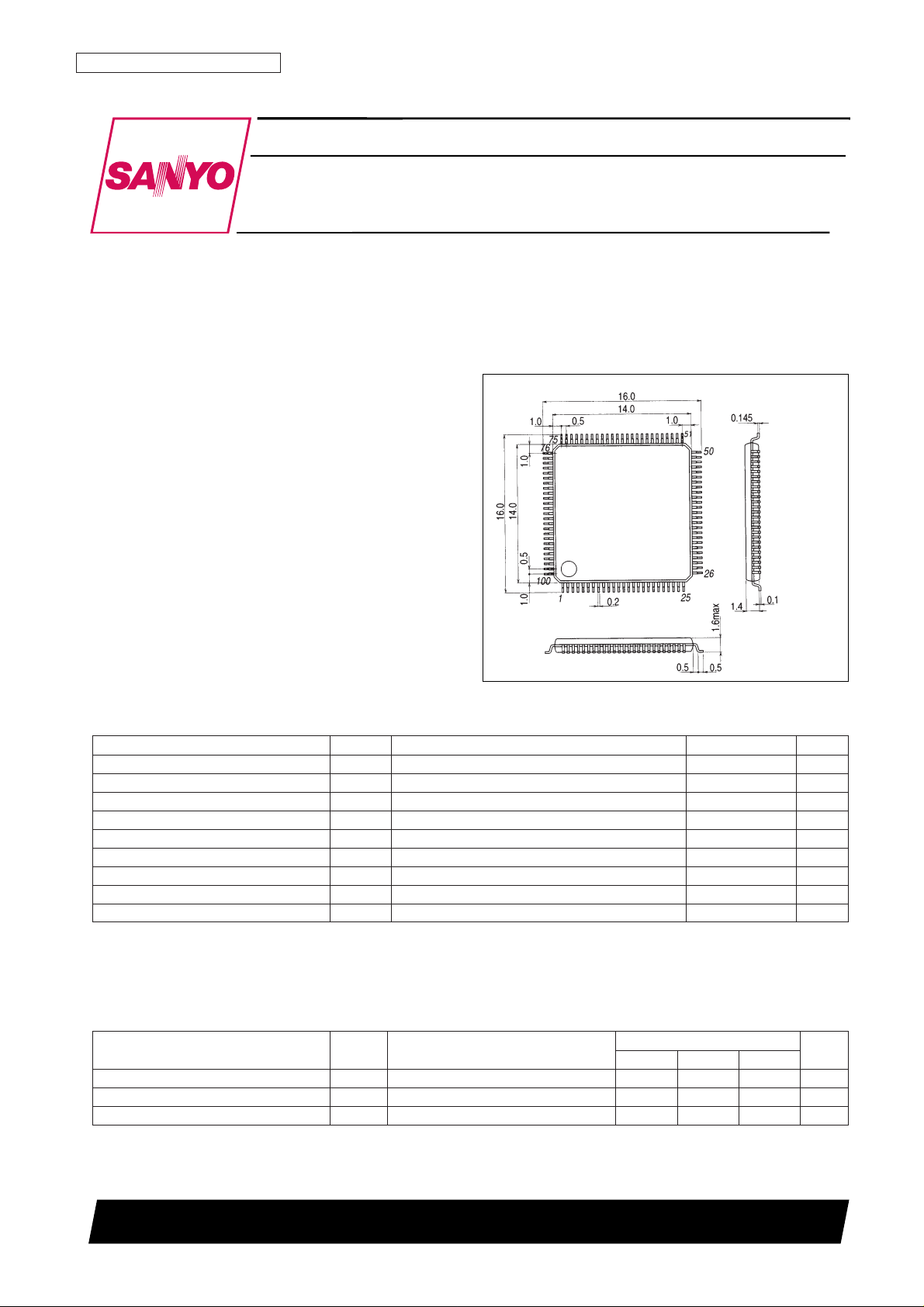
Package Dimensions
unit: mm
3181B-SQFP100
CMOS IC
51398RM (OT) No. 5787-1/8
SANYO: SQFP100
[LC99063-LF2]
SANYO Electric Co.,Ltd. Semiconductor Bussiness Headquarters
TOKYO OFFICE Tokyo Bldg., 1-10, 1 Chome, Ueno, Taito-ku, TOKYO, 110-8534 JAPAN
CCD Digital Signal Processing IC
LC99063-LF2
Ordering number : EN5787
Parameter Symbol Conditions Ratings Unit
Supply voltage V
DD
max –0.3 to +4.6 V
I/O voltage V
I
1, VOFor pin type 1 –0.3 to VDD+0.3 V
Input voltage V
I
2 For pin type 2 –0.3 to +7.3 V
Allowable power dissipation Pd max 400 mW
Operating temperature Topr –15 to +70 °C
Storage temperature Tstg –55 to +125 °C
Solder resistance (Hand soldering) 3s 350 °C
Solder resistance (Reflow) 10s 235 °C
I/O current Ii, Io * ±20 mA
Specifications
Absolute Maximum Ratings at VSS= 0 V
The pin types above refer to the following groups.
(1) DIN[32:9], DEVICE, MIRRO, SUPER, INMODE, WBHL, DOSL, SSET [2:1], OMODE [4:1], RES, DOUT [24:1], HREF, VDO, HDO, CLKOUT, ANA1,
ANA2, IREFOT1, IREFOT2, VREF1, VREF2, COMP1, COMP2
(2) DIN[8:1], CLK14M, CLK10M, HDI, VDI, HREF53, ENS, DATAS, CLKS, REGRES
*: This value is for a single I/O basic cell.
(1) DIN[32:9], DEVICE, MIRRO, SUPER, INMODE, WBHL, DOSL, SSET [2:1], OMODE [4:1], RES
(2) DIN[8:1], CLK14M, CLK10M, HDI, VDI, HREF53, ENS, DATAS, CLKS, REGRES
Parameter Symbol Conditions
Ratings
Unit
min typ max
Supply voltage V
DD
3 3.3 3.6 V
Input voltage range 1 Vin1 For pin type 1 0 V
DD
V
Input voltage range 2 Vin2 For pin type 2 0 +5.3 V
Allowable Operating Ranges at Ta = –15 to +70°C, VSS= 0 V
LC99063-LF2
Parameter Symbol Conditions
Ratings
Unit
min typ max
Input high-level voltage V
IH
CMOS level ; for pin type 1 0.7 V
DD
V
Input low-level voltage V
IL
CMOS level ; for pin type 1 0.2 V
DD
V
Input high-level voltage V
IH
CMOS level with Schmitt ; for pin type 2 0.75 V
DD
V
Input low-level voltage V
IL
CMOS level with Schmitt ; for pin type 2 0.15 V
DD
V
Output high-level voltage V
OHIOH
= –2 mA; for pin types 3 and 4 VDD– 0.8 V
Output low-level voltage V
OLIOL
= +2 mA; for pin types 3 and 4 0.4 V
Input leak current I
L
VI= VDD; for pin types 1 and 2 –10 +10 µA
Output leak current Ioz High-impedance output; for pin type 3 –10 +10 µA
Electrical Characteristics for Logic Circuits
DC Characteristics at Ta = –15 to +70°C, VDD= 3.0 to 3.6 V, VSS= 0 V
The pin types above refer to the following groups.
INPUT
(1) DIN [32:9], DEVICE, MIRRO, SUPER, INMODE, WBHL, DOSL, SSET [2:1], OMODE [4:1], RES
(2) DIN [8:1], CLK14M, CLK10M, HDI, VDI, HREF53, ENS, DATAS, CLKS, REGRES
OUTPUT
(3) DOUT [24:1]
(4) HREF, VDO, HDO, CLKOUT
Note: The ANA1, ANA2, IREFOT1, IREFOT2, VREF1, VREF2, COMP1, and COMP2 pins fall outside these DC characteristic specifications.
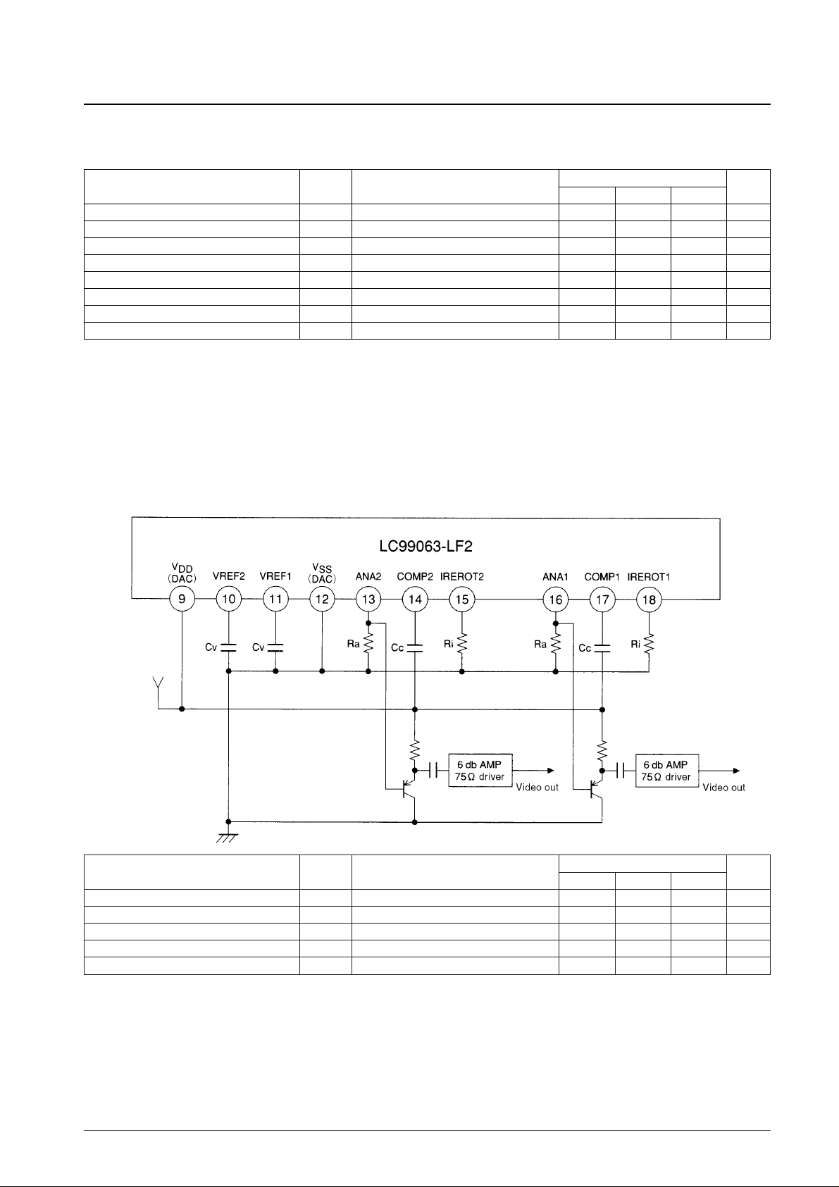
Electrical Characteristics for Analog Circuits
Recommended operating conditions for D/A converter
Parameter Symbol Conditions
Ratings
Unit
min typ max
Reference voltage VREF1/2 1.11 V
Analog output resistance Ra 200 Ω
Reference voltage resistance Ri Ra
× 4 Ω
Phase compensation capacitor Cc 0.1 µF
VREF capacitor Cv 0.1 µF
No. 5787-2/8
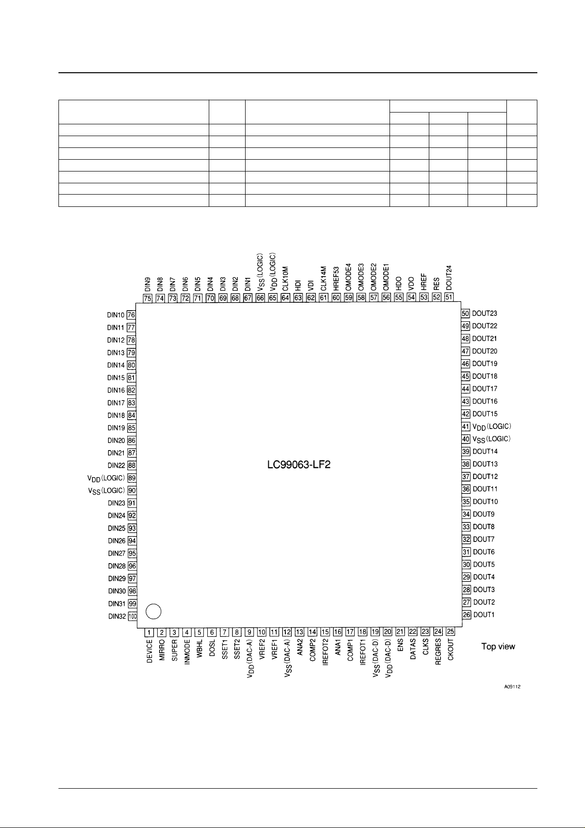
Pin Assignment
No. 5787-3/8
LC99063-LF2
Parameter Symbol Conditions
Ratings
Unit
min typ max
Resolution 8 Bits
Conversion frequency 15 MSPS
Zero scale output voltage –15 0 +15 mV
Full scale output voltage 1.01 1.1 1.19 V
Linearity error ±1.0 LSB
Differential linearity error ±0.5 LSB
Reference output voltage 1.09 1.1 1.11 V
Electrical Characteristics for D/A Converter at Ta = 25°C, VDD= 3.3 V, Rv = 200 Ω, Ri = 800 Ω
 Loading...