

SANYO LC99012A-S Datasheet
Ordering number : EN*5281A
22896HA (OT) No. 5281-1/6
Overview
The LC99012A-S is a timing generator for the 1/5-inch
LC9947G and LC9948G and the 1/6-inch LC9949G
black-and-white CCD image sensors.
Features
• 5 V single-voltage power supply
• Generates all pulses required for CCD drivers.
• Generates all pulses required for video signal
processing.
• Built-in synchronizing signal generator that supports
both EIA and CCIR.
• Includes buffer circuits for directly driving the CCD
horizontal transfer and reset gates.
• Includes light metering and control systems for an
automatic electronic iris function.
• Fixed rate-of-change control allows a smooth electronic
iris function to be implemented (an iris state output is
provided).
• Supports AGC control and a light metering mode that
compensates for backlighting.
• Selectable CCD storage mode (non-interlaced or
interlaced)
• Selectable TV scan mode (non-interlaced or interlaced)
• Allows all types of external synchronization.
• Built-in EXT-C.SYNC sync separator circuit
• Built-in phase comparator for external synchronization
• Control from external electronic shutter pulses and
frame shift pulses supports one-shot imaging.
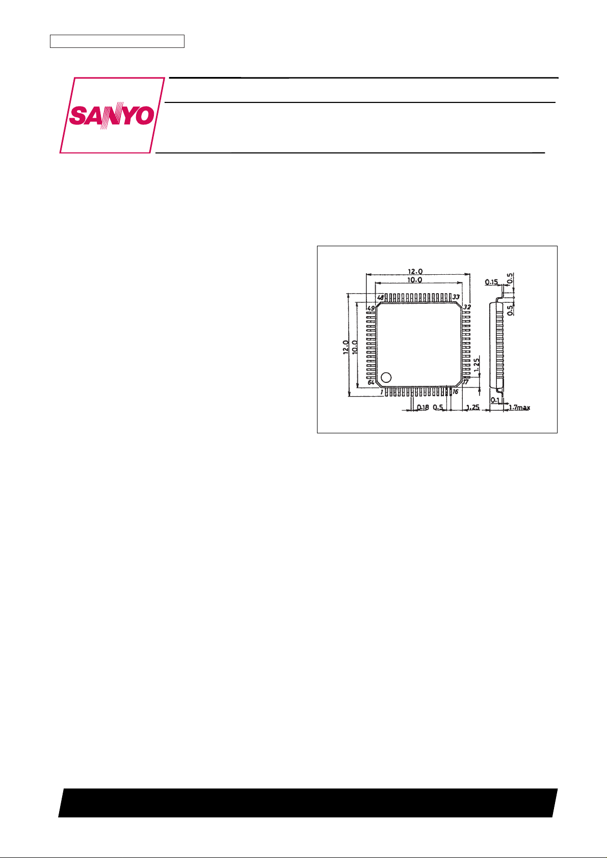
• Package: 0.5 mm lead pitch flat package (SQFP-64)
• Flickerless function
• Sensitivity-increasing function
Package Dimensions
unit: mm
3190-SQFP64
Preliminary
SANYO: SQFP64
[LC99012A-S]
LC99012A-S
SANYO Electric Co.,Ltd. Semiconductor Bussiness Headquarters
TOKYO OFFICE Tokyo Bldg., 1-10, 1 Chome, Ueno, Taito-ku, TOKYO, 110-8534 JAPAN
Black-and-White CCD Timing Generator
CMOS LSI
Specifications
Absolute Maximum Ratings at VSS= 0 V
Note: * Per individual I/O reference cell
Allowable Operating Ranges at Ta = –30 to +65°C, VSS= 0 V
DC Characteristics: Input and Output Levels at VSS= 0 V, VDD= 4.5 to 5.5 V, Ta = –30 to +65°C
See the note on next page.
No. 5281-2/6
LC99012A-S
Parameter Symbol Conditions Ratings Unit
Maximum supply voltage V
DD
max –0.3 to +7.0 V
Input and output voltages V
I
, V
O
–0.3 to VDD+ 0.3 V
Allowable power dissipation Pd max Ta ≤ 65°C 290 mW
Operating temperature Topr –30 to +65 °C
Storage temperature Tstg –55 to +125 °C
Soldering heat resistance
Hand soldering: 3 seconds 350 °C
Reflow soldering: 10 seconds 235 °C
Input and output currents I
I
, I
O
±20* mA
Parameter Symbol Conditions min typ max Unit
Supply voltage V
DD
4.5 5.0 5.5 V
Input voltage range V
IN
0 V
DD
V
Parameter Symbol Conditions min typ max Unit
Input high-level voltage V
IH
1 TTL levels: (6) 2.2 V
Input low-level voltage V
IL
1 TTL levels: (6) 0.8 V
Input high-level voltage V
IH
2 CMOS levels: (1), (3) 0.7 V
DD
V
Input low-level voltage V
IL
2 CMOS levels: (1), (3) 0.3 V
DD
V
Input high-level voltage V
IH
3 CMOS levels, Schmitt inputs: (4) 0.8 V
DD
V
Input low-level voltage V
IL
3 CMOS levels, Schmitt inputs: (4) 0.2 V
DD
V
Input high-level voltage V
IH
4 CMOS levels, inputs with pull-up resistors: (2) 0.7 V
DD
V
Input low-level voltage V
IL
4 CMOS levels, inputs with pull-up resistors: (2) 0.3 V
DD
V
Input high-level voltage V
IH
5 CMOS levels, inputs with pull-up resistors: (5) 0.7 V
DD
V
Input low-level voltage V
IL
5 CMOS levels, inputs with pull-up resistors: (5) 0.3 V
DD
V
Output high-level voltage V
OH
1 IOH= –3 mA: (6), (13), (14), (15) VSS– 2.1 V
Output low-level voltage V
OL
1 IOL= 3 mA: (6), (13), (14), (15) 0.4 V
Output low-level voltage V
OL
2 IOL= 3 mA: (9) 0.4 V
Output high-level voltage V
OH
3 IOH= –6 mA: (12) VDD– 2.1 V
Output low-level voltage V
OL
3 IOL= 6 mA: (12) 0.4 V
Output high-level voltage V
OH
4 IOH= –6 mA: (7) VDD– 2.1 V
Output low-level voltage V
OL
4 IOL= 2 mA: (7) 0.4 V
Output high-level voltage V
OH
5 IOH= –30 mA: (11) VDD– 2.1 V
Output low-level voltage V
OL
5 IOL= 10 mA: (11) 0.4 V
Output high-level voltage V
OH
6 IOH= –12 mA: (8) VDD– 2.1 V
Output low-level voltage V
OL
6 IOL= 12 mA: (8) 0.4 V
Output high-level voltage V
OH
6 IOH= –12 mA: (10) VDD– 1.5 V
Output low-level voltage V
OL
7 IOL= 6 mA: (8) 0.4 V
Input leakage current I
IL
VI= VSS, VDD: (1), (3), (4), (6) –10 +10 µA
Output leakage current I
OZ
In high-impedance output mode: (6), (9), (13) –10 +10 µA
Pull-up resistance R
UP
(2) 10 20 40 kΩ
Pull-down resistance R
DN
(5) 25 50 100 kΩ
 Loading...