

SANYO LC89977M Datasheet
Overview
The LC89977M is CCD delay line for PAL television
system that includes a chrominance signal crosstalk
exclusion filter and a luminance signal 1-H delay line on
chip.
Features
• 5-V single-voltage power supply
• Built-in 3 × PLL frequency multiplier circuit allows 3fsc
operation from an fsc (4.43 MHz) input.
• Can be switched between the PAL/GBI, and 4.43NTSC
formats by setting control pin values.
• Includes a built-in crosstalk exclusion comb filter for the
chrominance signal that provides high-precision comb
characteristics in an adjustment-free circuit.
• Peripheral circuits provided on chip for operation with a
minimum of external components.
• Positive-phase signal input, positive-phase signal output
(luminance signal)
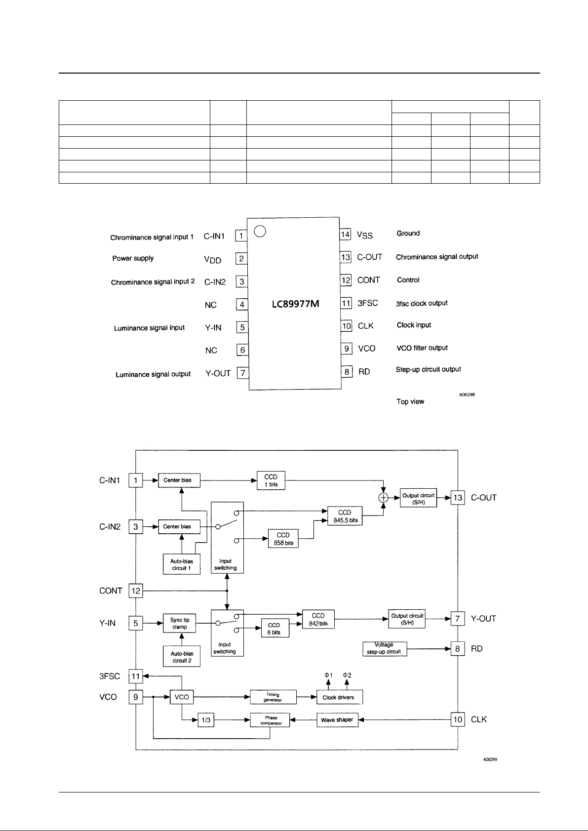
Functions
• CCD shift registers (for chrominance and luminance
signals)
• Timig generator and clock driver for CCD
• Delay time selective circuit
• CCD signal adder
• Auto-bias circuit
• Sync tip clamp circuit (luminance signal)
• Center bias circuit (chrominance signal)
• Sample-and-hold circuit
•3 ×PLL frequency multiplier circuit
• 3fsc clock output circuit
• High voltage generator for CCD Reset Drain (RD)
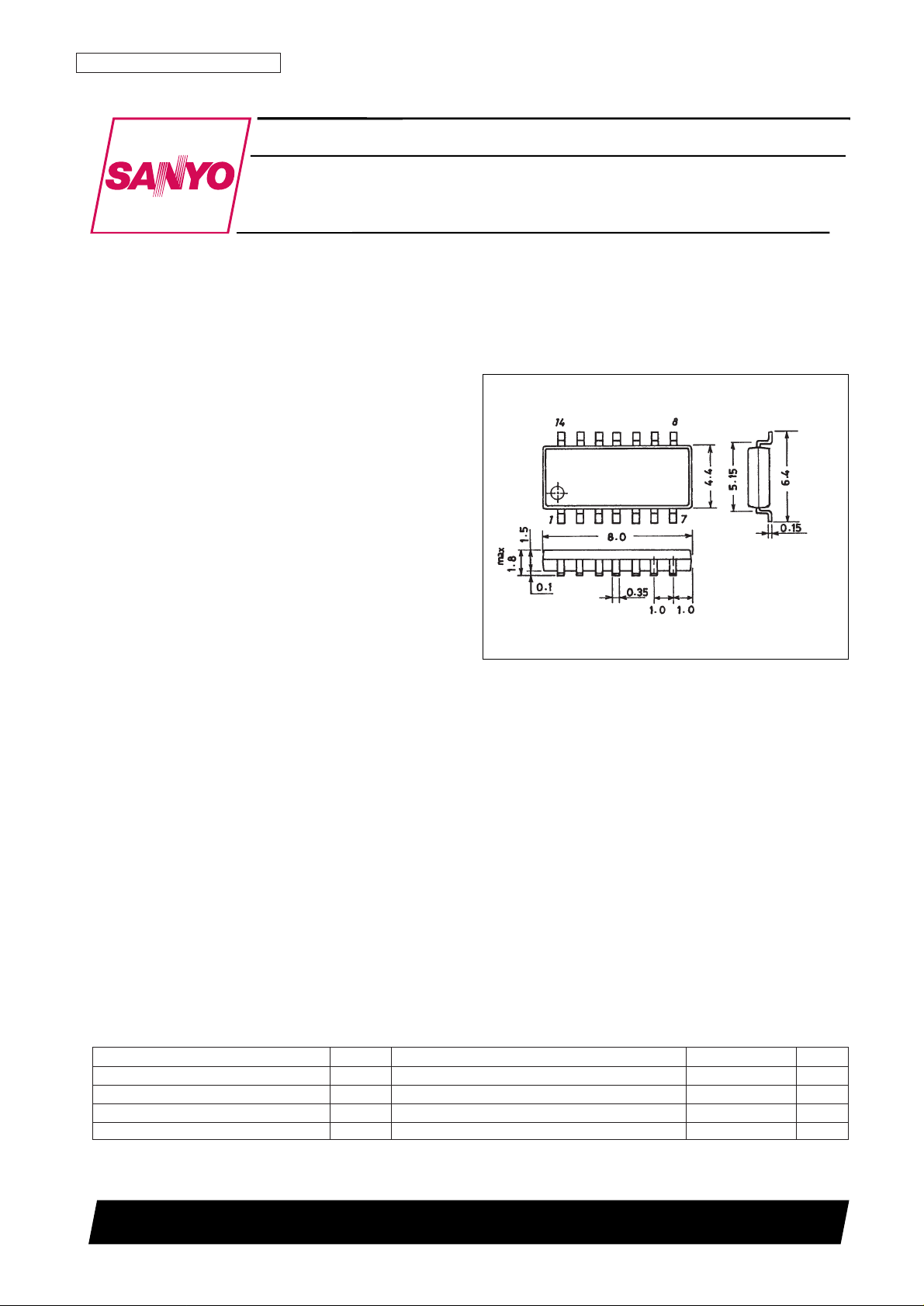
Package Dimensions
unit: mm
3111-MFP14S
MOS LSI
N3096HA(OT) No. 5545-1/7
Preliminary
SANYO: MFP14S
[LC89977M]
SANYO Electric Co.,Ltd. Semiconductor Bussiness Headquarters
TOKYO OFFICE Tokyo Bldg., 1-10, 1 Chome, Ueno, Taito-ku, TOKYO, 110 JAPAN
CCD Delay Line for PAL
LC89977M
Ordering number : EN5545
Parameter Symbol Conditions Ratings Unit
Supply voltage V
DD
–0.3 to +6.0 V
Allowable power dissipation Pd max 250 mW
Operating temperature Topr –10 to +60 °C
Storage temperature Tstg –55 to +125 °C
Specifications
Absolute Maximum Ratings at Ta = 25°C
No. 5545-2/7
LC89977M
Parameter Symbol Conditions
Ratings
Unit
min typ max
Supply voltage V
DD
4.75 5.00 5.25 V
Clock input amplitude V
CLK
300 500 1000 mVp-p
Clock frequency F
CLK
Sine wave 4.43361875 MHz
Chrominance signal input amplitude V
IN-C
350 500 mVp-p
Luminance signal input amplitude V
IN-Y
400 572 mVp-p
Allowable Operating Ranges at Ta = 25°C
Pin Assignment
Block Diagram
No. 5545-3/7
LC89977M
CONT Mode (representative) Chrominance signal delay (number of CCD stages) Luminance signal delay (number of CCD stages)
Low PAL/GBI 2H (1703.5) + 0H (1) 1H (848)
High 4.43NTSC 1H (845.5) + 0H (1) 1H (842)
Control Pin Functions
Parameter Symbol Conditions
Ratings
Unit
min typ max
Switching voltage level: low V
L
–0.3 0.0 +0.5 V
Switching voltage level: high V
H
2.0 5.0 6.0 V
Switching Voltage Levels
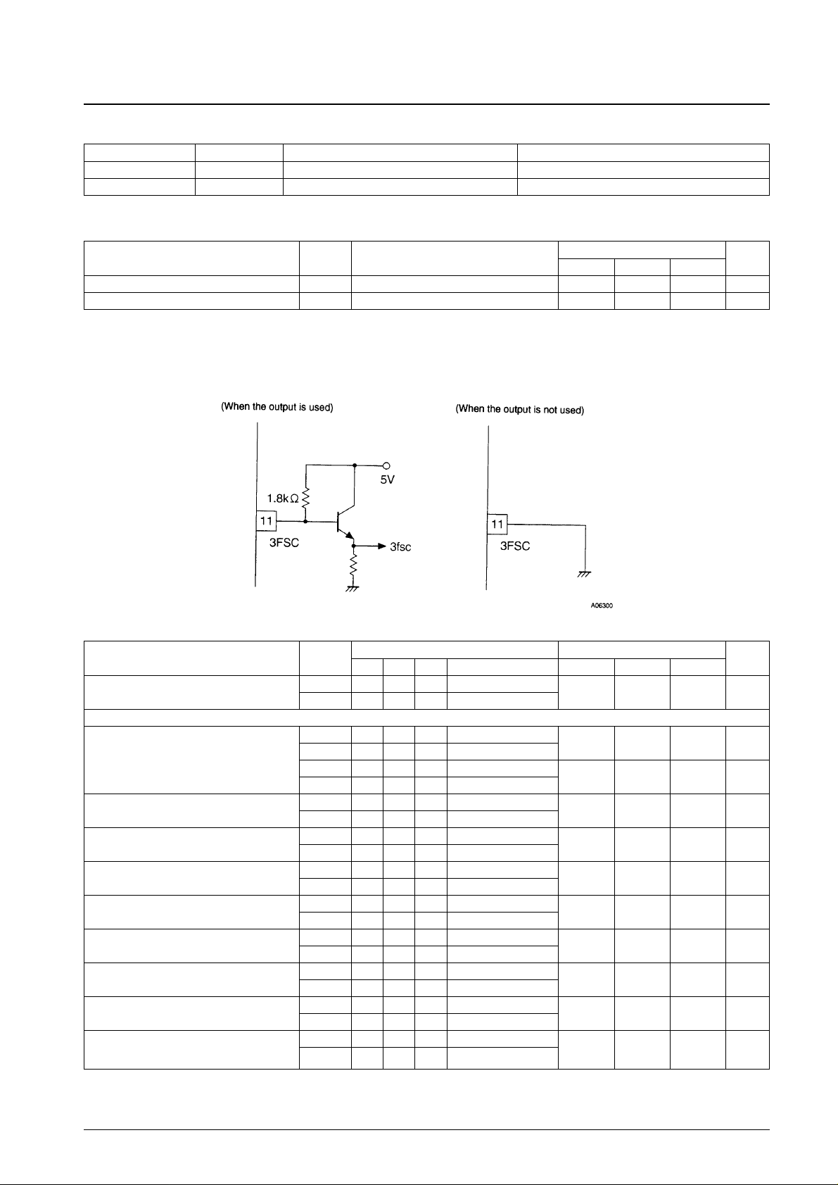
Function of the 3FSC Pin
This pin provides a 3fsc clock signal generated by the 3 × PLL frequency multiplier circuit.
Note: *Since the control pins have built-in pull-down resistors (about 70 kΩ), leaving these pins opens effectively sets them to the low level.
Continued on next page.
Parameter Symbol
Switch states Ratings
Unit
SW1 SW2 SW3 Test conditions min typ max
I
DD-1
a a b *1
Supply current
I
DD-2
b a b *1
27 32 37 mA
[Chrominance signal characteristics] (with no input to Y-IN)
V
INC-1
a a b *2
DC output voltage
V
INC-2
b a b *2
1.9 2.4 2.9 V
V
OUTC-1
a a b *2
V
OUTC-2
b a b *2
1.4 1.9 2.4 V
G
VC-1
a a b *3
Voltage gain
G
VC-2
b a b *3
–2 0 +2 dB
C
D-1
a a b *4
Comb depth
C
D-2
b a b *4
–40 –35 dB
L
NC-1
a a b *5
Linearity
L
NC-2
b a b *5
–0.3 0.0 +0.3 dB
L
CK3C-1
a a b *6
Clock leakage (3fsc)
L
CK3C-2
b a b *6
10 50 mVrms
L
CK1C-1
a a b *6
Clock leakage (fsc)
L
CK1C-2
b a b *6
0.5 1.5 mVrms
N
C-1
a a b *7
Noise
N
C-2
b a b *7
0.5 2.0 mVrms
Z
OC-1
a a a, b *8
Output impedance
Z
OC-2
b a a, b *8
200 350 500 Ω
T
DC-1
a a b *9
0-H delay time
T
DC-2
b a b *9
130 ns
Electrical Characteristics at VDD= 5.0 V, Ta = 25°C, F
CLK
= 4.43361875 MHz, V
CLK
= 500 mVp-p
 Loading...