

Ordering number : EN*5391
41596HA (OT) No. 5391-1/7
Overview
The LC89975M is a lower-cost PAL-Format CCD delay
line based on the LC89970M, with the sizes of chip and
package miniaturized and the external parts count reduced.
Features
• 5 V single-voltage power supply
• On-chip 3× PLL circuit for 3·fsc operation from an fsc
(4.43 MHz) input
• Supports PAL/GBI and 4.43 NTSC systems, selected by
a control pin input
• Includes an on-chip comb filter for chrominance signal
crosstalk exclusion. This adjustment-free circuit
provides high-precision comb characteristics.
• Peripheral circuits included on chip to allow operation
with minimal external circuits.
• Positive-phase signal input, positive phase signal output
(luminance signal)
Functions
• CCD shift register (for chrominance and luminance
signals)
• CCD drive circuit
• Circuit for switching the number of CCD stages
• CCD signal addition circuit
• Auto-bias circuit
• Sync tip clamping circuit (luminance signal)
• Center bias circuit (chrominance signal)
• Sample-and-hold circuit
• PLL 3× circuit
• 3·fsc clock output circuit
• RD voltage generation step-up circuit
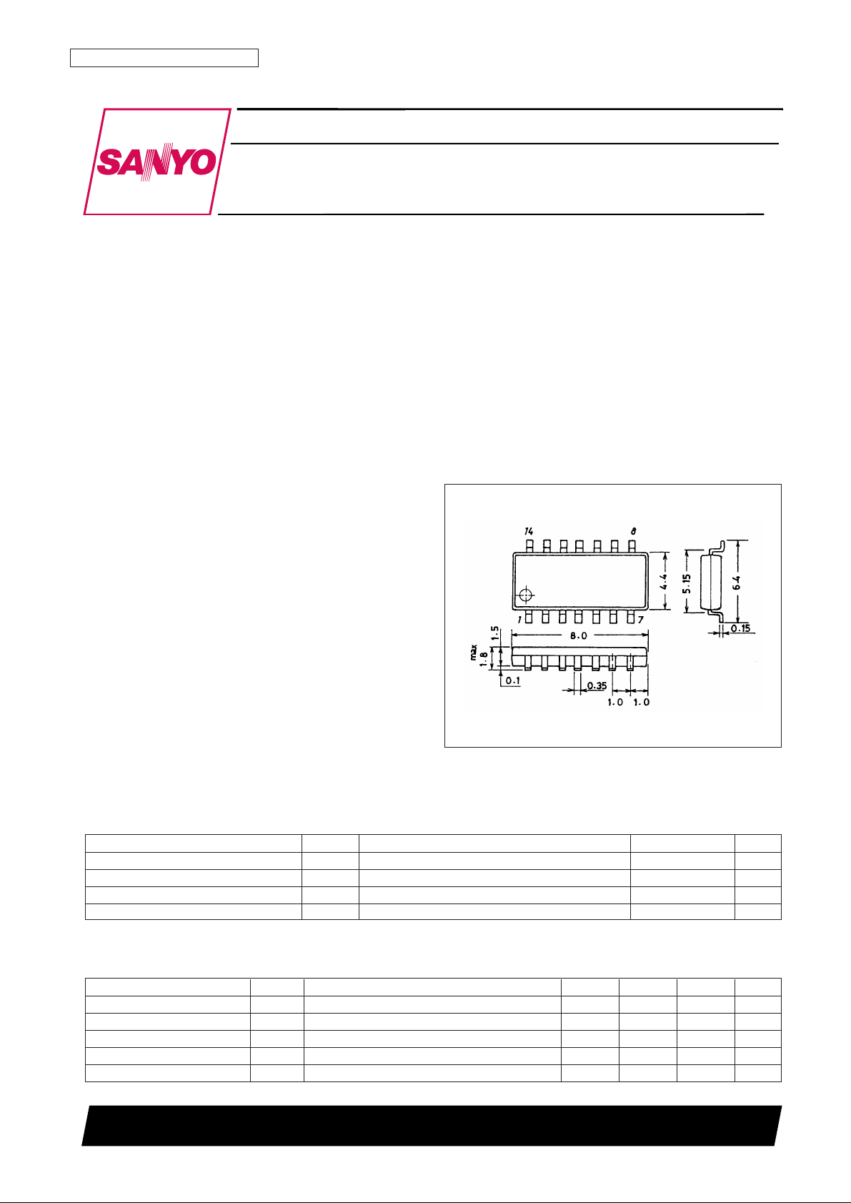
Package Dimensions
unit: mm
3111-MFP14S
Preliminary
SANYO: MFP14S
[LC89975M]
LC89975M
SANYO Electric Co.,Ltd. Semiconductor Bussiness Headquarters
TOKYO OFFICE Tokyo Bldg., 1-10, 1 Chome, Ueno, Taito-ku, TOKYO, 110-0005 JAPAN
PAL-Format Delay Line
NMOS + CCD
Specifications
Absolute Maximum Ratings at Ta = 25°C
Recommended Conditions at Ta = 25°C
Parameter Symbol Conditions Ratings Unit
Supply voltage V
DD
–0.3 to +6.0 V
Allowable power dissipation Pdmax 250 mW
Operating temperature Topr –10 to +60 °C
Storage temperature Tstg –55 to +150 °C
Parameter Symbol Conditions min typ max Unit
Supply voltage V
DD
4.75 5.00 5.25 V
Clock input amplitude V
CLK
300 500 1000 mVp-p
Clock frequency F
CLK
Sine wave — 4.43361875 — MHz
Chrominance signal input amplitude V
IN-C
— 350 500 mVp-p
Luminance signal input amplitude V
IN-Y
— 400 572 mVp-p
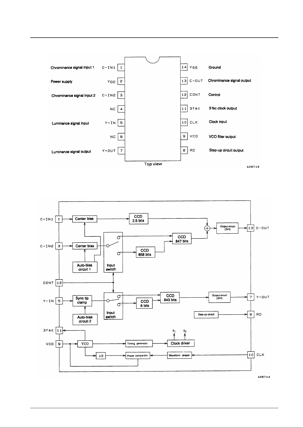
Pin Assignment
Block Diagram
No. 5391-2/7
LC89975M
Control Pin
Switching levels
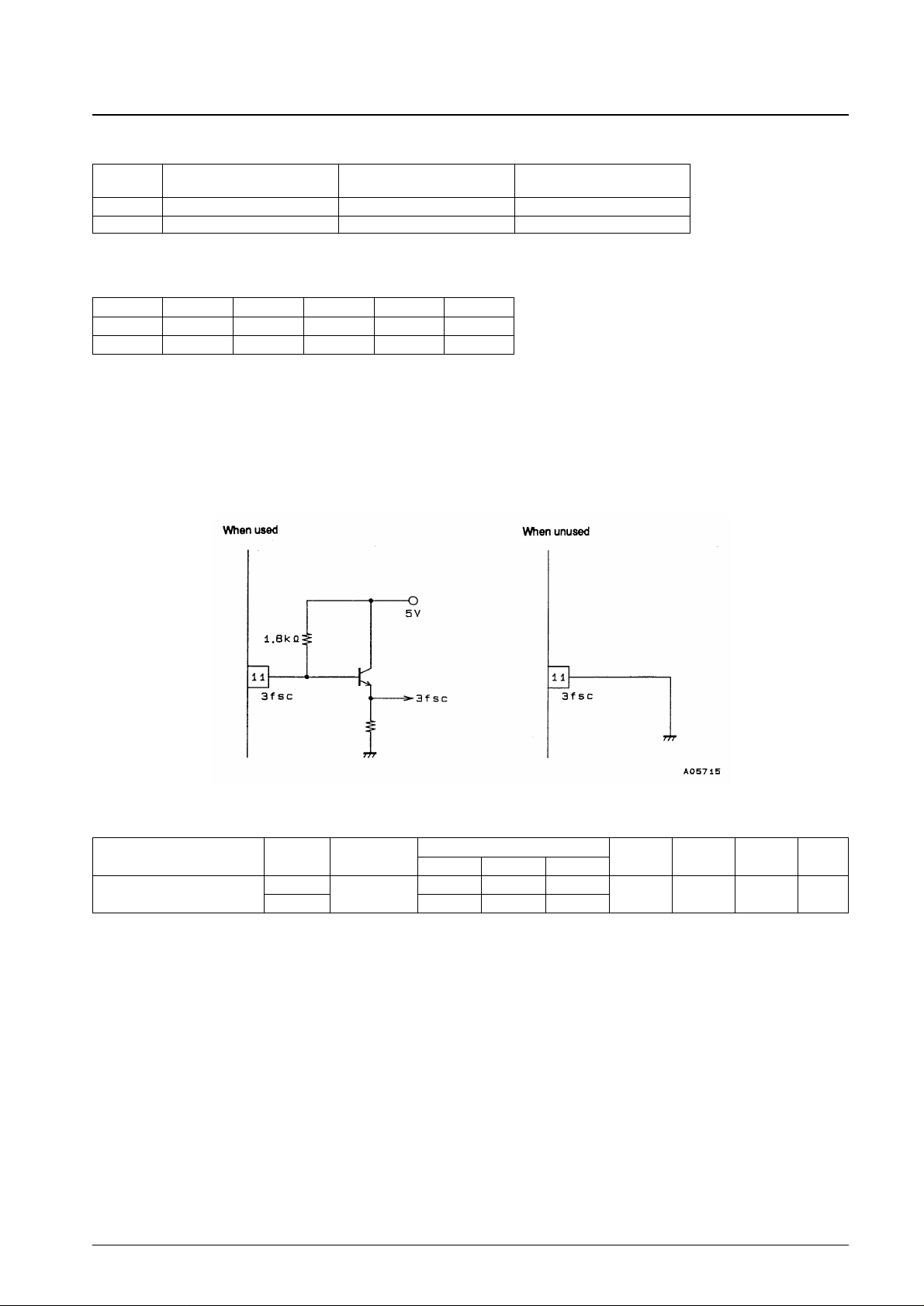
Note: Since a pull-down resistor of about 70 kΩ is built in the control pin circuit, it will remain fixed at the low level if
left open.
3fsc Pin
This pin outputs the 3·fsc clock signal generated by the PLL 3× circuit.
Electrical Characteristics at VDD= 5.0 V, Ta = 25°C, F
CLK
= 4.43361875 MHz, V
CLK
= 500 mVp-p
No. 5391-3/7
LC89975M
CONT
Mode Chrominance signal delay Luminance signal delay
(typical example) (number of CCD stages) (number of CCD stages)
Low PAL/GBI 2H (1705) + 0H (2.5) 1H (849)
High 4.43 NTSC 1H (847) + 0H (2.5) 1H (843)
Low/High Symbol min typ max Unit
Low V
L
–0.3 0.0 +0.5 V
High V
H
2.0 5.0 6.0 V
Parameter Symbol Test conditions
Switch states
min typ max Unit
SW1 SW2 SW3
Power-supply current
I
DD-1
1
a a b
27 32 37 mA
I
DD-2
b a b
 Loading...