

SANYO LC89972M Datasheet
Ordering number : EN 51134465
72595TH (OT) No. 5113-1/8
Overview
The LC89972M is a CCD delay line for PAL television
systems. It incorporates a comb filter for chrominance signal
and a 1H delay line for luminance signal.
Structure
• NMOS + CCD
Functions
• Two CCD shift registers (for chrominance and
luminance signals)
• CCD drive circuits
• CCD stage count switching circuit
• CCD signal adder
• Auto-bias circuit
• Sync tip clamping circuit (luminance signal)
• Center-bias circuit (chrominance signal)
• Sample-and-hold circuit
• PLL 3 × frequency multiplier
• 3 fsc clock output circuit
• RD voltage generator
Features
• 5 V single-voltage power supply
• Built-in PLL 3 × frequency multiplier circuit allows
3 fsc operation from an fsc (4.43 MHz) input.
• Control pin switchable to handle PAL/GBI and
4.43 MHz NTSC systems.
• Built-in chrominance signal crosstalk exclusion comb
filter features high-precision comb characteristics in an
adjustment-free circuit.
• Built-in peripheral circuits allow applications to be
constructed with a minimum number of external
components.
• Positive-phase signal input/positive-phase signal output
(luminance signal)
Specifications
Absolute Maximum Ratings at Ta = 25°C
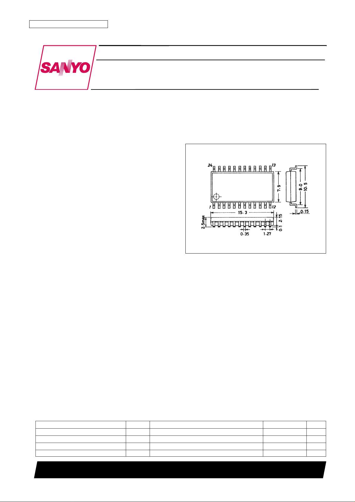
Package Dimensions
unit: mm
3045B-MFP24
SANYO: MFP24
[LC89972M]
LC89972M
SANYO Electric Co.,Ltd. Semiconductor Bussiness Headquarters
TOKYO OFFICE Tokyo Bldg., 1-10, 1 Chome, Ueno, Taito-ku, TOKYO, 110-8534 JAPAN
PAL CCD Delay Line
MOS IC
Parameter Symbol Conditions Ratings Unit
Maximum supply voltage V
DD
max –0.3 to +6.0 V
Allowable power dissipation Pd max 600 mW
Operating temperature Topr –10 to +70 °C
Storage temperature Tstg –55 to +150 °C
Allowable Operating Ranges at Ta = 25°C
Electrical Characteristics at Ta = 25°C, VDD= 5.0 V, F
CLK
= 4.43361875 MHz, V
CLK
= 500 mVp-p
No. 5113-2/8
LC89972M
Parameter Symbol Conditions min typ max Unit
Supply voltage V
DD
4.75 5.00 5.25 V
Clock input amplitude V
CLK
300 500 1000 mVp-p
Clock frequency F
CLK
Sine wave — 4.43361875 — MHz
Clock signal input amplitude V
IN-C
— 350 500 mVp-p
Luminance signal input amplitude V
IN-Y
— 400 572 mVp-p
Parameter Symbol
Switch states
Conditions min typ max Unit
SW1 SW2 SW3
Supply current
I
DD-1
a a b
1 40 50 60 mA
I
DD-2
b a b
Chrominance System Characteristics (with no Y-IN input)
Pin voltage (input)
V
INC-1
a a b
2.0 2.4 2.8 V
V
INC-2
b a b
2
Pin voltage (output)
V
OUTC-1
a a b
1.2 1.6 2.0 V
V
OUTC-2
b a b
Voltage gain
G
VC-1
a a b
3 –2 0 +2 dB
G
VC-2
b a b
Comb depth
C
D-1
a a b
4 — –40 –35 dB
C
D-2
b a b
Linearity
L
NC-1
a a b
5 –0.3 0.0 +0.3 dB
L
NC-2
b a b
Clock leakage (3 fsc)
L
CK3C-1
a a b
— 10 50 mVrms
L
CK3C-2
b a b
6
Clock leakage (fsc)
L
CK1C-1
a a b
— 0.8 1.5 mVrms
L
CK1C-2
b a b
Noise
N
C-1
a a b
7 — 0.5 2.0 mVrms
N
C-2
b a b
Output impedance
Z
OC-1
a a a, b
8 200 350 500 Ω
Z
OC-2
b a a, b
0 H delay time
T
DC-1
a a b
9 — 245 — ns
T
DC-2
b a b
Continued from preceding page.
Test Conditions
1. Supply current with no signal input
2. C-OUT voltage (center bias voltage) with no signal input.
3. Measure the C-OUT output with 350 mVp-p sine wave signals input to C-IN1 and C-IN2.
GVC= 20 log [dB]
Test frequencies
GVC-1 4.429662 MHz (PAL/GBI)
GVC-2 4.425694 MHz (4.43 NTSC)
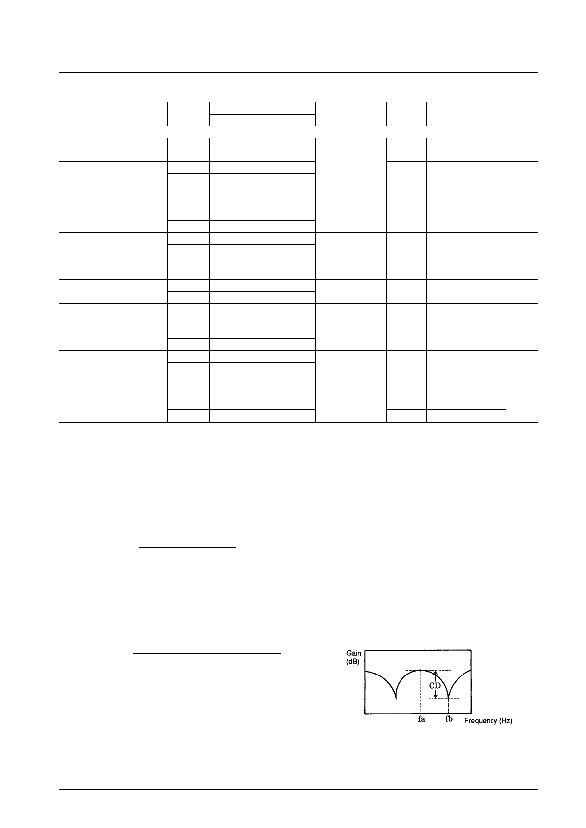
4. Measure the comb depth from the C-OUT output with a 350 mVp-p sine wave signal of frequency fa input to C-IN1
and C-IN2 and with a frequency of fb input.
CD= 20 log [dB]
Test frequencies
fa fb
CD-1 4.429662 MHz 4.425756 MHz (PAL/GBI)
CD-2 4.425694 MHz 4.417819 MHz (4.43 NTSC)
C-OUT output with fb input [mVp-p]
C-OUT output with fa input [mVp-p]
C-OUT output [mVp-p]
350 [mVp-p]
No. 5113-3/8
LC89972M
Parameter Symbol
Switch states
Conditions min typ max Unit
SW1 SW2 SW3
Luminance System Characteristics (with no C-IN1 or C-IN2 input)
Pin voltage (input)
V
INY-1
a a b
1.7 2.1 2.5 V
V
INY-2
b a b
10
Pin voltage (output)
V
OUTY-1
a a b
0.8 1.2 1.6 V
V
OUTY-2
b a b
Voltage gain
G
VY-1
a a b
11 –2 0 +2 dB
G
VY-2
b a b
Frequency response
G
FY-1
a b b
12 –2 0 +2 dB
G
FY-2
b b b
Differential gain
D
GY-1
a a b
0 5 7 %
D
GY-2
b a b
13
Differential phase
D
PY-1
a a b
0 5 7 deg
D
PY-2
b a b
Linearity
L
SY-1
a a b
14 37 40 43 %
L
SY-2
b a b
Clock leakage (3 fsc)
L
CK3Y-1
a a b
— 10 50 mVrms
L
CK3Y-2
b a b
15
Clock leakage (fsc)
L
CK1Y-1
a a b
— 0.8 1.5 mVrms
L
CK1Y-2
b a b
Noise
N
Y-1
a a b
16 — 0.5 2.0 mVrms
N
Y-2
b a b
Output impedance
Z
OY-1
a a c, b
17 250 400 550 Ω
Z
OY-2
b a c, b
Delay time
T
DY-1
a a b
18
— 63.92 —
µs
T
DY-2
b a b — 63.47 —
 Loading...