

CMOS LSI
Ordering number : EN*5420
93096HA (OT) No. 5420-1/6
SANYO Electric Co.,Ltd. Semiconductor Bussiness Headquarters
TOKYO OFFICE Tokyo Bldg., 1-10, 1 Chome, Ueno, Taito-ku, TOKYO, 110 JAPAN
NTSC Format Delay Line
LC89962, LC89962M
Overview
The LC89962 and LC89962M are delay line circuits that
provide a delayed signal by a 1H period of NTSC format
with an external low-pass filter.
Features
• Requires only the input of a 3.58-MHz clock to produce
a 1H delayed signal and the external low-pass filter.
• Uses a 5-V single-voltage power supply.
• Requires a minimal number of external components due
to the peripheral components provided on chip.
• Output signal has the same phase as the input signal.
• Operation has a 4fsc clock synchronized with the input
clock allows these products to be used as wide
bandwidth delay lines.
• A 4fsc clock can be output from the 4FSC pin (pin 7).
Functions
• 906-bit CCD shift register
• Timing generator and CCD driver circuits
• Auto-bias circuit
• Sync-tip clamp circuit
• Sample-and-hold and output amplifier circuits
•4 × PLL circuit
• 4fsc output circuit
Specifications
Absolute Maximum Ratings at Ta = 25°C
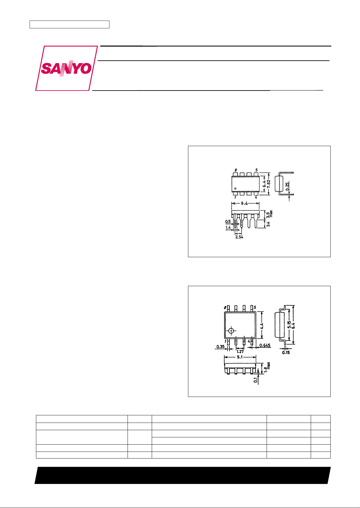
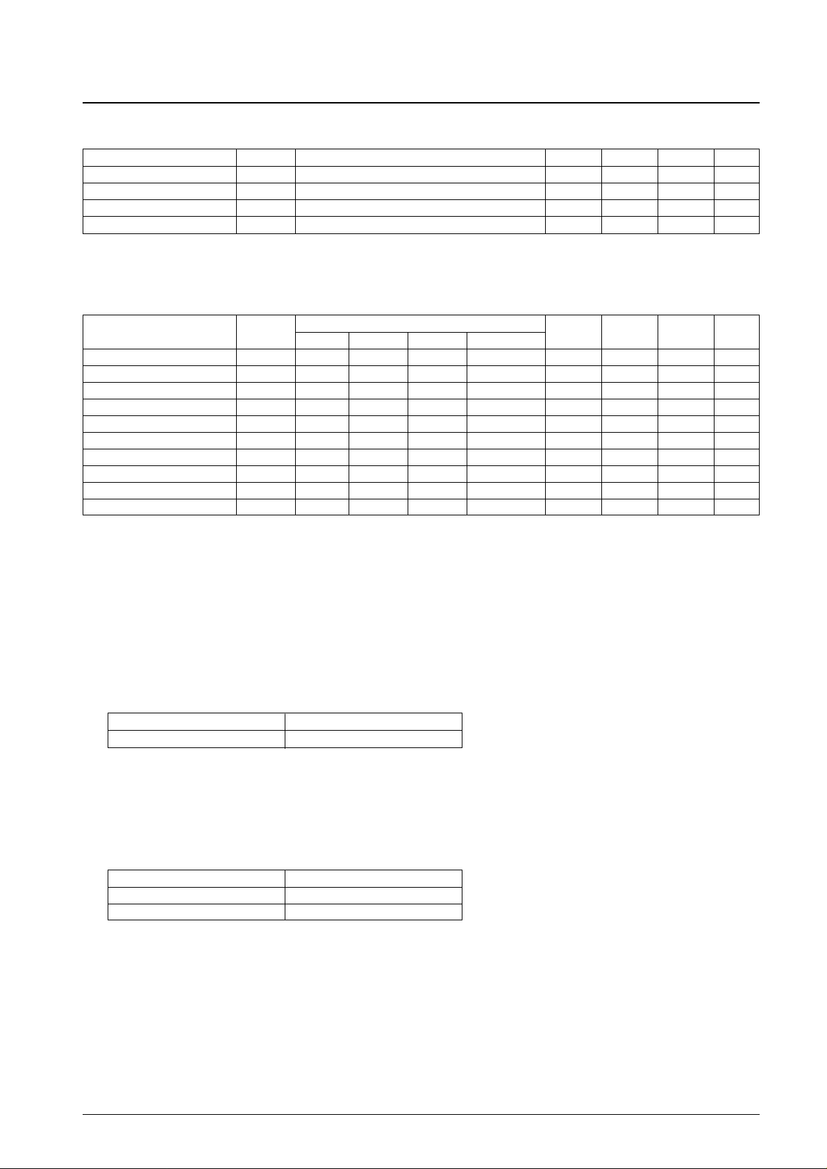
Package Dimensions
unit: mm
3001B-DIP8
unit: mm
3032B-MFP8
SANYO: DIP8
[LC89962]
SANYO: MFP8
[LC89962M]
Parameter Symbol Conditions Ratings Unit
Supply voltage V
DD
–0.3 to +6.0 V
Allowable power dissipation Pd max
LC89962 400 mW
LC89962M 140 mW
Operating temperature Topr –10 to +60 °C
Storage temperature Tstg –55 to +125 °C
Allowable Operating Ranges at Ta = 25°C
Note 1. The input signal must be input with low impedance for correct operation of sync-tip clamping.
Electrical Characteristics at Ta = 25°C, VDD= 5.0 V, CLK = 3.579545 MHz; 300 mV p-p
Test Conditions
1. The supply current with no input signal
2. The following formula is used to calculate the voltage gain (GV).
V
OUT
[mVp-p]
GV= 20log ——————— [dB]
500 [mVp-p]
3. The following formula is used to calculate the frequency characteristics (Gf).
V2 [mVp-p]
Gf= 20log —————— [dB]
V1 [mVp-p]
During this test, adjust Vbias so that the input signal DC level is 250 mV higher than the clamp level.
No. 5420-2/6
LC89962, LC89962M
Parameter Symbol
Switch states
min typ max Unit
SW1 SW2 SW3 Test conditions
Supply current I
DD
a a a *1 5 15 25 mA
Voltage gain G
V
a b a *2 –2 0 +2 dB
Frequency characteristics G
f
b b a *3 –2 –1 0 dB
Differential gain DG a a a *4 0 5 %
Differential phase DP a a a *4 0 5 deg
Linearity LS a a a *5 37 40 43 %
Clock leakage Lck a b a *6 5 50 mVrms
Noise N
O
a b a *7 1 2 mVrms
Output impedance Z
O
a b a↔b *8 220 370 520 Ω
Delay time TD a b a *9 63.33 µs
Parameter Symbol Conditions min typ max Unit
Supply voltage V
DD
4.75 5.0 5.25 V
Clock input amplitude V
CLK
Sine wave 200 300 500 mVp–p
Clock frequency F
CLK
3.579545 MHz
Signal input amplitude V
IN
(*1) 500 572 mVp–p
Output signal symbol Input signal
V
OUT
Sine wave: 200 kHz, 500 mV p-p
Output signal symbol Input signal
V1 Sine wave: 200 kHz, 200 mV p-p
V2 Sine wave: 3.58 MHz, 200 mV p-p
 Loading...