SANYO LC8991 Datasheet

Ordering number: EN3202A
Overview
The Sanyo LC8991 is a 1H delay line for NTSC television
systems.
NTSC CCD 1H Delay Line
.
Sample-and-hold circuit
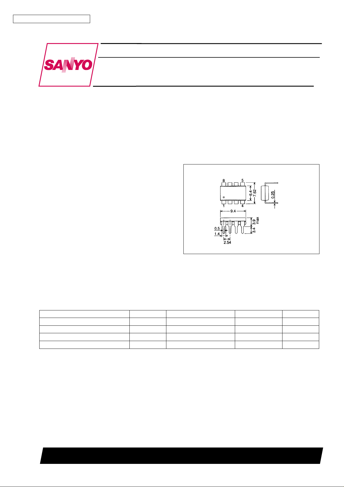
Package Dimensions
unit : mm
LC8991
Features
.
Single 9 V power supply
.
Low clock input voltage
.
1H delay signal can be obtained with low-pass filter and
7.16 MHz clock input
.
Minimum number of external components required because
timing generator, driver, bias generator and output amplifier
are built in
.
8-pin DIP (Small package)
3001B-DIP8
[LC8991]
Functions
.
453 stages CCD shift register
.
CCD drive circuit
.
Auto-bias circuit
.
Sync tip clamp circuit
SANYO : DIP8
Specifications
Absolute Maximum Ratings at Ta = 25°C
Parameter Symbol Conditions Ratings Unit
Maximum supply voltage V
Allowable power dissipation Pd max 500 mW
Operating temperature Topr –10 to +60 °C
Storage temperature Tstg –55 to +125 °C
max 11 V
DD
SANYO Electric Co.,Ltd. Semiconductor Bussiness Headquarters
TOKYO OFFICE Tokyo Bldg., 1-10, 1 Chome, Ueno, Taito-ku, TOKYO, 110 JAPAN
13097HA(II)/N090JN, JK/8290TA No.3202-1/4

LC8991
Electrical Characteristics
Parameter Symbol Conditions min typ max Unit
DC Characteristics at Ta = 25°C, V
Supply voltage V
Supply current I
DC output voltage
AC Characteristics at Ta = 25°C, V
Maximum input voltage V
Voltage gain VG Input : 15 kHz, 0.5 Vp-p 6 9 11 dB
Linearity
Frequency response Gf Note 2 –3.0 –2.3 dB
Noise V
Clock input voltage Eck 0.1 0.3 1.0 Vp-p
Output impedance Z
Delay time t
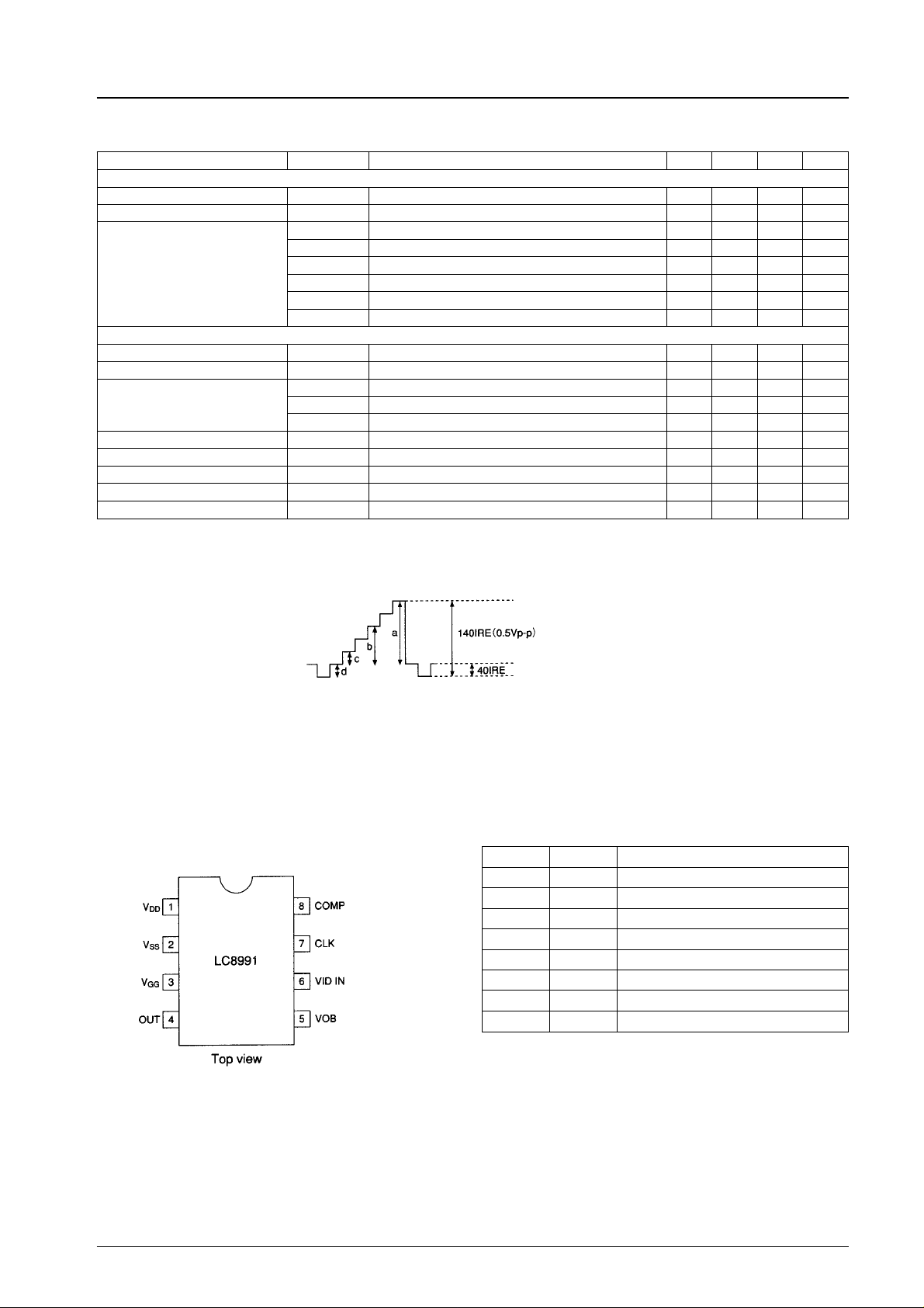
Note 1) Linearity test
Input: 5 step staircase signal
= 9 V, CLOCK = 7.15909 MHz; 0.3 Vp-p
DD
DD
DD
V
GG
OUT 3.1 V
VOB 4.5 V
VID IN 2.8 V
CLK 2.0 V
COMP 2.7 V
= 9 V, CLOCK = 7.15909 MHz ; 0.3 Vp-p
DD
max 0.5 0.7 Vp-p
IN
L6 b/a, Note 1 56 60 64 %
L2 c/a, Note 1 18 20 22 %
LS d/a, Note 1 37 40 43 %
NO
O
3.4 MHz bandwidth 1.1 mVrms
O
8.5 9.0 9.5 V
16.5 20.0 mA
13.5 V
520 Ω
63.42 µs
Note 2) Frequency response test
Input = 0.5 Vp-p sine wave (2.4 MHz)/(20 kHz)
Pin Assignment Pin Description
Pin No. Symbol Function
1V
2V
3V
4 OUT Delay signal output
5 VOB Feedback output
6 VID IN Signal input
7 CLK Clock input
8 COMP Duty cycle compensation output
DD
SS
GG
Power supply
GND
VGGvoltage output
No.3202-2/4
 Loading...