

SANYO LC89902V Datasheet
Overview
The LC89902V is a vertical driver CMOS IC specifically
designed for use with VGA-format CCD image sensors.
Applications
• Image input units and similar products
Features
•
CMOS structure supporting low power dissipation.
• Level shifter circuits provided on chip to minimize the
number of external components required.
• Miniature package (24-pin SSOP)
Functions
• Inverting drivers: 6 channels
— Converts input pulses to VCC1, VCC2, and VCC3, as
well as VEE1 and VEE2 levels (inverting).
— Generates the drive levels required for the image
sensor imaging and storage sections.
• Inverting drivers: 2 channels
— These drivers convert input pulses to VCC1, VCC2,
and VCC3, as well as VEE1 and VEE2 levels
(inverting).
— These drivers generate the drive levels required for
the image sensor transfer gate.
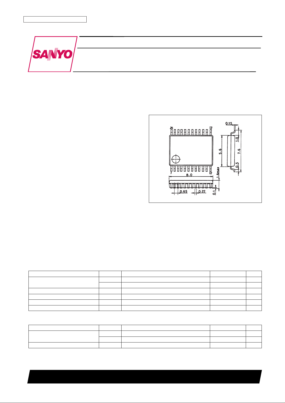
Package Dimensions
unit: mm
3175A-SSOP24
CMOS LSI
Ordering number : EN5741
93097HA (OT) No. 5741-1/5
SANYO Electric Co.,Ltd. Semiconductor Bussiness Headquarters
TOKYO OFFICE Tokyo Bldg., 1-10, 1 Chome, Ueno, Taito-ku, TOKYO, 110 JAPAN
CMOS Driver for VGA-Format Image Sensors
LC89902V
Specifications
Absolute Maximum Ratings at Ta = 25°C
Allowable Operating Ranges at Ta = 25°C
[LC89902V]
SANYO: SSOP24
Parameter Symbol Condition Ratings Unit
Maximum supply voltage
V
CC
max VCC1, VCC2, VCC3 –0.3 to +6.0 V
V
EE
max VEE1, VEE2 –11.0 to +0.3 V
Input and voltages V
IN
All input pins –0.3 to VCC+ 0.3 V
Allowable power dissipation Pd max 350 mA
Operating temperature Topr –10 to +70 °C
Storage temperature Tstg –40 to +125 °C
Parameter Symbol Conditions Ratings Unit
Supply voltage
V
CC
VCC1, VCC2, VCC3 4.5 to 5.5 V
V
EE
VEE1, VEE2 –10.5 to 0 V
Input voltage range V
IN
All input pins 0 to V
CC
V

No. 5741-2/5
LC89902V
Block Diagram
 Loading...