

SANYO LC89901V Datasheet
Overview
The LC89901V is a high breakdown voltage CMOS
vertical driver IC for 1/5 and 1/6 inch image sensors.
Provision of a built-in level shifter means that an external
clamp circuit is no longer required.
Applications
Surveillance cameras and image input equipment
Functions
CMOS driver IC for 1/5 and 1/6 inch image sensors
Features
• CMOS process fabrication for low power dissipation
• Built-in level shifter circuits to reduce the number of
required peripheral circuits.
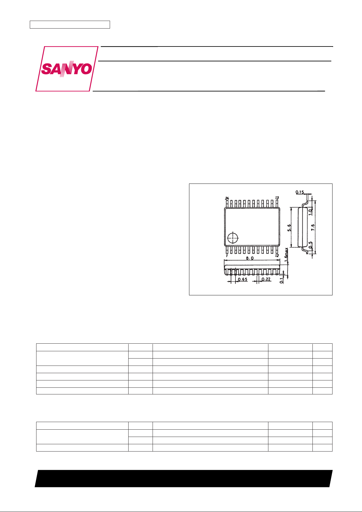
• Miniature package (SSOP-24)
Structure
• Inverter type drivers: 8 channels
Input pulses are converted to VCC1, VCC2 and VEE1,
VEE2 levels (inversion).
These are drivers for image sensor imaging and storage
sections.
• Inverter type driver: 1 channel
Input pulses are converted to VCCN and VEE1, VEE2
levels (inversion).
This circuit is an image sensor NSUB driver.
Package Dimensions
unit: mm
3175A-SSOP24
CMOS LSI
Ordering number : EN5078A
73097HA (OT)/32895TH (OT) NO. 5078-1/4
SANYO: SSOP24
[LC89901V]
SANYO Electric Co.,Ltd. Semiconductor Bussiness Headquarters
TOKYO OFFICE Tokyo Bldg., 1-10, 1 Chome, Ueno, Taito-ku, TOKYO, 110 JAPAN
CMOS Driver IC for 1/5 and 1/6 Inch
Image Sensors
LC89901V
Specifications
Absolute Maximum Ratings at Ta = 25°C
Allowable Operating Ranges at Ta = 25°C
Parameter Symbol Conditions Ratings Unit
Maximum supply voltage
V
CC
max VCC1, VCC2, VCCN –0.3 to +6.0 V
V
EE
max VEE1, VEE2 +0.3 to –11.0 V
Input voltage V
IN
All input pins –0.3 to VCC+ 0.3 V
Allowable power dissipation Pd max 350 mA
Operating temperature Topr –10 to +70 °C
Storage temperature Tstg –40 to +125 °C
Parameter Symbol Conditions Ratings Unit
Supply voltage
V
CC
VCC1, VCC2, VCCN : *VCCN ≤ VCC1, VCC2 4.5 to 5.5 V
V
EE
VEE1, VEE2 0 to –10.5 V
Input voltage range V
IN
All input pins 0 to V
CC
V
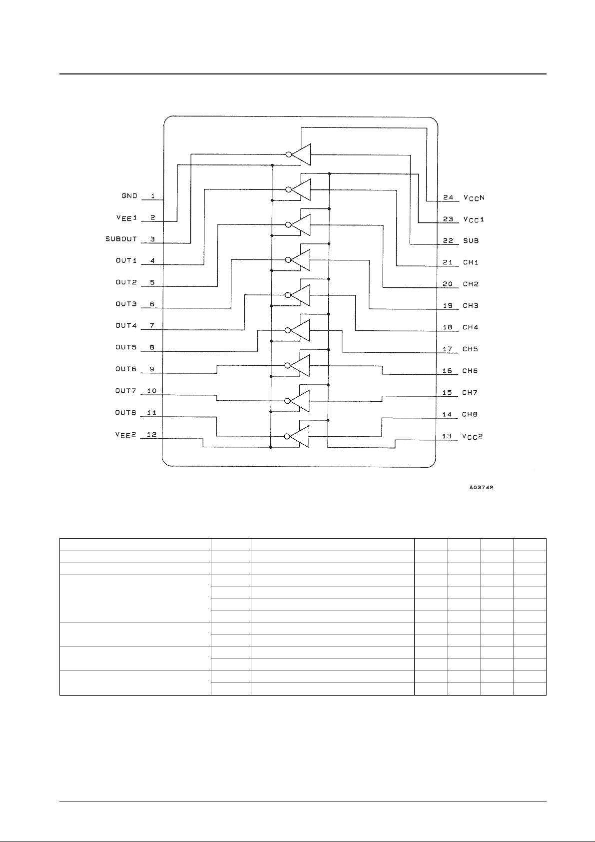
Block Diagram
Electrical Characteristics at Ta = 25°C, VCC1, VCC2, VCCN = 5.0 V, VEE1, VEE2 = –10.0 V
Note: Load conditions
Load circuit
* Reference values for driving an LC9997 image sensor with pulses input from an LC99052 timing LSI.
NO. 5078-2/4
LC89901V
Parameter Symbol Conditions min typ max Unit
Input high level current I
IH
All input pins, VIN= 5.0 V 10 µA
Input low level current I
IL
All input pins, VIN= 0 V 5 nA
I
CCH
+ V
CC
1, VCC2, VCCN, all input pins, VIN= 5.0 V 1 µA
Current drain
I
CCH
– V
EE
1, VEE2, all input pins, VIN= 5.0 V –10 µA
I
CCL
+ V
CC
1, VCC2, VCCN, all input pins, VIN= 0 V 7 µA
I
CCH
– V
EE
1, VEE2, all input pins, VIN= 0 V –2 µA
Output voltage
V
OH
All inputs, VIN= 0 V 5.0 V
V
OL
All inputs, VIN= 5.0 V –10.0 V
Operating output voltage*
V
OH
2 Load = LC9997, input = LC99052 5.0 V
V
OL
2 Load = LC9997, input = LC99052 –10.0 V
Operating current drain*
I
CC
2+Load = LC9997, input = LC99052 1.62 mA
I
CC
2–Load = LC9997, input = LC99052 1.61 mA
RL= 18 Ω, CL= 780 pF
 Loading...