

CMOS LSI
Ordering number : *EN5572
22897HA (OT) No. 5572-1/11
Preliminary
LC897194
SANYO Electric Co.,Ltd. Semiconductor Bussiness Headquarters
TOKYO OFFICE Tokyo Bldg., 1-10, 1 Chome, Ueno, Taito-ku, TOKYO, 110 JAPAN
CD-ROM Decoder with Built-In ATAPI (IDE) and DVD
ECC Interfaces
Overview
The LC897194 provides CD-ROM functionality and
includes built-in DVD ECC and ATAPI (IDE) interfaces.
Function
• CD-ROM ECC functionality, an ATAPI (IDE) interface
(the register and other blocks), and a DVD ECC
interface
Features
• ATAPI (IDE) interface
• DVD ECC interface
• Supports up to 12×-speed playback (when using 70-ns
16-bit data path DRAM)
• Transfer rate: 16.6 MB/s (when using 60-ns 16-bit data
path DRAM)
• Transfer rate: 8.33 MB/s (when using 70-ns 8-bit data
path DRAM)
• Between 1 and 32 Mbits of DRAM can be used as buffer
RAM.
• The user can freely set up the CD main channel and the
C2 flags in buffer RAM.
• Built-in batch transfer function (function for transferring
the CD main channel and the C2 flags in one operation)
• Built-in multiple transfer function (function for
automatically transferring multiple blocks in a single
operation)
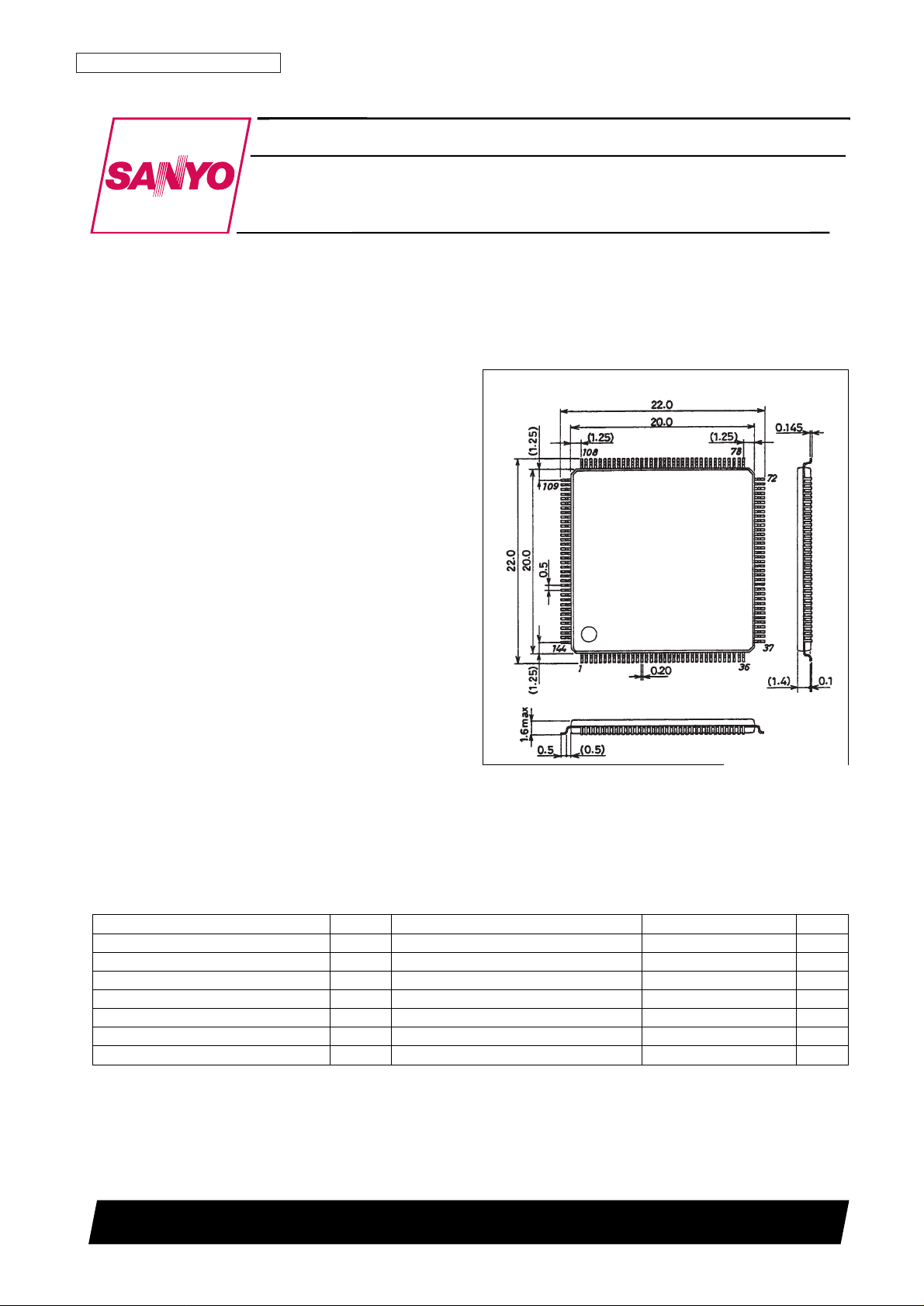
Package Dimensions
unit: mm
3214-SQFP144
SANYO: SQFP144
[LC897194]
Parameter Symbol Conditions Ratings Unit
Maximum supply voltage V
DD
max Ta = 25°C –0.3 to +7.0 V
I/O voltages V
I
, VOTa = 25°C –0.3 to VDD+0.3 V
Allowable power dissipation Pd max Ta ≤ 70°C 550 mW
Operating temperature Topr –30 to +70 °C
Storage temperature Tstg –55 to +125 °C
Soldering heat resistance (pins only) 10 seconds 235 °C
Maximum I/O power I
I
, IOmax ±20* mA
Specifications
Absolute Maximum Ratings at VSS= 0 V
Note: Per basic I/O cell.
No. 5572-2/11
LC897194
Parameter Symbol Applicable pins (see below)
Ratings
Unit
min typ max
Input high-level voltage V
IH1
TTL compatible: (1) 2.2 V
Input low-level voltage V
IL1
TTL compatible: (1) 0.8 V
Input high-level voltage V
IH2
TTL compatible, with pull-up resistor: (12) 2.2 V
Input low-level voltage V
IL2
TTL compatible, with pull-up resistor: (12) 0.8 V
Input high-level voltage V
IH3
TTL compatible, with pull-down resistor: (2) 2.2 V
Input low-level voltage V
IL3
TTL compatible, with pull-down resistor: (2) 0.8 V
Input high-level voltage V
IH4
TTL compatible, Schmitt characteristics: (3),
2.5 V
(5), (13), (14)
Input low-level voltage V
IL4
TTL compatible, Schmitt characteristics: (3),
0.6 V
(5), (13), (14)
Input high-level voltage V
IH5
CMOS compatible, Schmitt characteristics: (4) 0.8 V
DD
V
Input low-level voltage V
IL5
CMOS compatible, Schmitt characteristics: (4) 0.2 V
DD
V
Output high-level voltage V
OH1IOH
= –2 mA : (7), (10), (12) VDD– 2.1 V
Output low-level voltage V
OL1IOL
= 2 mA : (7), (10), (12) 0.4 V
Output high-level voltage V
OH2IOH
= –8 mA : (6) VDD– 2.1 V
Output low-level voltage V
OL2IOL
= 8 mA : (6) 0.4 V
Output high-level voltage V
OH3IOH
= –4 mA : (8), (13) VDD– 2.1 V
Output low-level voltage V
OL3IOL
= 24 mA : (8), (13) 0.4 V
Output high-level voltage V
OH4IOL
= 24 mA : (9), (14) 0.4 V
Output low-level voltage V
OL5IOL
= 2 mA : (11) 0.4 V
Input leakage current I
IL
VI= VSS, VDD: (1), (2), (3), (4), (5), (12), (13),
–10 +10 µA
(14)
Output leakage current I
OZ
When the output is high impedance: (9), (11),
–10 +10 µA
(13), (14)
Pull-up resistance R
UP
(12) 40 80 160 kΩ
Pull-down resistance R
DN
(2) 40 80 160 kΩ
DC Characteristics at Ta = –30 to +70°C, VSS= 0 V, VDD= 4.5 to 5.5 V
Note: The applicable pins are as follows:
INPUT
(1) CSCTRL, RSSEL, HDB0 to 7, SUA0 to 6
(2) TEST0 to 4
(3) ZDMACK, ZHRST, ZRESET, BCK, C2PO, LRCK, SDATA, DA0 to 2, ZCS1FX, ZCS3FX
(4) ZCS, ZRD, ZWR
(5) ZDIOR, ZDIOW, DRESP, WFCK, SCOR
OUTPUT
(6) MCK, MCK2
(7) ZINT0, ZINT1
(8) DMARQ, HINTRQ
(9) IORDY, ZIOCS16
(10) RA0 to 9, ZCAS0 to 1, ZRAS0 to 1, ZLWE, ZUWE, ZOE, DREQ
(11) ZRSTCPU, ZRSTIC, ZSWAIT
INOUT
(12) D0 to 7, IO0 to 15
(13) DD0 to 15
(14) ZDASP, ZPDIAG
*: The DC characteristics do not apply to the XTAL and XTALCK pins.
Parameter Symbol Conditions
Ratings
Unit
min typ max
Supply voltage V
DD
4.5 5.0 5.5 V
Input voltage range V
IN
0 V
DD
V
Allowable Operating Ranges at Ta = –30 to +70°C, VSS= 0 V

Recommended Oscillator Circuit Example
R1 = 120 kΩ
R2 = 47 Ω
C1 = 30 pF
With a crystal with a resonant frequency of 16.9344 MHz, or:
R1 = 3.3 kΩ
R2 = None
C1 = 5 pF
With a crystal with a resonant frequency of 33.8688 MHz.
If third harmonics are a problem in the 33.8688-MHz recommended circuit, consult with the manufacturer of the crystal
for exact component values, since those values will be influenced by the printed circuit board used.
No. 5572-3/11
LC897194

Block Diagram
*1 BCK, SDATA, LRCK, C2PO
*2 DD0 to DD15, ZDASP, ZPDIAG
*3 ZCS1FX, ZCS3FX, DA0 to DA2, ZDIOR, ZDIOW, ZDMACK
*4 DMARQ, HINTRQ, ZIOCS16, IORDY, ZHRST
*5 ZRD, ZWR, SUA0 to SUA6, ZCS, CSCTRL
*6 D0 to D7
*7 IO0 to IO15
*8 RA0 to RA9, ZRAS0, ZRAS1, ZCAS0, ZCAS1, ZOE, ZUWE, ZLWE
*9 DREQ
*10 HDB0 to HDB7, DRESP
*11 WFCK, SCOR
**1 HISIDE (WD25C32) is made by WESTERN DIGITAL.
No. 5572-4/11
LC897194
 Loading...