


Ordering number : ENN6251
N3099TH (OT) No. 6251-1/14
Overview
The LC897127K is a CD-ROM decoder that includes an
on-chip DVD interface. Since the LC897127K also
includes an on-chip SCSI interface, it can be used to
implement a SCSI-compatible DVD-ROM drive simply
by combining it with a DVD decoder. It can also operate
as an independent SPC functional unit.
Functions
• CD-ROM ECC function, subcode read function, SCSI
I/F, CAV audio function, DVD I/F
• ATAPI-to-SCSI conversion function, DMA I/F-to-SCSI
conversion function
Features
• Built-in SCSI I/F (Built-in register for SCAM selection)
•20× speed and transfer speed of 10 Mbytes/s supported
using EDO-DRAM (×16, 70 ns)
•32× speed and transfer speed of 10 Mbytes/s supported
using EDO-DRAM (16×, 50 ns)
• Up to 4 Mbits of buffer RAM connectable
• CD main channel and C2 flag areas in buffer RAM can
be freely set by user
• Built-in batch transfer function (function for sending CD
main channel, C2 flag, etc. at one time)
• Built-in multi block transfer function (function for
sending several blocks at one time)
• Built-in subcode buffering function and CD text support
• Built-in CAV audio function
• 20 Mbytes/s transfer supported
• Built-in DVD I/F
• Built-in ATAPI I/F-to-SCSI conversion function
• Built-in DMA I/F-to-SCSI conversion function
Package Dimensions
unit: mm
3214-SQFP144
LC897127K
SANYO Electric Co.,Ltd. Semiconductor Company
TOKYO OFFICE Tokyo Bldg., 1-10, 1 Chome, Ueno, Taito-ku, TOKYO, 110-8534 JAPAN
SCSI CD-ROM Decoder
with On-Chip DVD Interface
CMOS IC
0.20
1.25
1.25
22.0
20.0
0.5
22.0
20.0
0.5
1.25
1.25
0.145
0.1
1.4
1.6max
0.5
0.5
136
37
72
73
108
109
144
SANYO: SQFP144
[LC897127K]
Any and all SANYO products described or contained herein do not have specifications that can handle
applications that require extremely high levels of reliability, such as life-support systems, aircraft’s
control systems, or other applications whose failure can be reasonably expected to result in serious
physical and/or material damage. Consult with your SANYO representative nearest you before using
any SANYO products described or contained herein in such applications.
SANYO assumes no responsibility for equipment failures that result from using products at values that
exceed, even momentarily, rated values (such as maximum ratings, operating condition ranges, or other
parameters) listed in products specifications of any and all SANYO products described or contained
herein.
No. 6251-2/14
LC897127K
Parameter Symbol Conditions Ratings Unit
Maximum supply voltage V
DD
max Ta = 25°C –0.3 to +7.0 V
Input/output voltage V
IVO
Ta = 25°C –0.3 to VDD+0.3 V
Allowable power dissipation Pd max Ta ≤ 70°C 550 mW
Operating temperature Topr –30 to +70 °C
Storage temperature Tstg –55 to +125 °C
Soldering temperature (pin part only) 10s 260 °C
Specifications
Absolute Maximum Ratings at VSS= 0 V
Parameter Symbol Conditions
Ratings
Unit
min typ max
Supply voltage V
DD
4.5 5.0 5.25 V
Input voltage range V
IN
0V
DD
V
Allowable Operating Ranges at Ta = –30 to +70°C, VSS= 0 V
Parameter Symbol Conditions Applicable pins
Ratings
Unit
min typ max
Input high-level voltage V
IH1
TTL levels (1)
2.2 V
Input low-level voltage V
IL1
0.8 V
Input high-level voltage V
IH2
TTL levels
(9)
2.2——V
Input low-level voltage V
IL2
with pull-up resistor — — 0.8 V
Input high-level voltage V
IH3
TTL levels
(2)
2.2——V
Input low-level voltage V
IL3
Schmitt — — 0.8 V
Input high-level voltage V
IH3
TTL levels
(11)
2.2——V
Input low-level voltage V
IL3
Schmitt with pull-down resistor — — 0.8 V
Input high-level voltage V
IH4
TTL levels
(12)
2.2——V
Input low-level voltage V
IL4
Schmitt with pull-up resistor — — 0.8 V
Input high-level voltage V
IH4
CMOS levels
(3)
0.8 V
DD
——V
Input low-level voltage V
IL4
Schmitt — — 0.2 V
DD
V
Input high-level voltage VI
H5
(4), (8), (10)
2.0 — V
Input low-level voltage V
IL5
0.8 V
Output high-level voltage V
OH1IOH1
= –12 mA
(6)
VDD– 2.1 — — V
Output low-level voltage V
OL1IOL1
= 12 mA — — 0.4 V
Output high-level voltage V
OH2IOH2
= –8 mA
(7), (11)
2.4 — V
Output low-level voltage V
OL2IOL2
= 8 mA 0.4 V
Output high-level voltage V
OH2IOH2
= –2 mA
(9), (5)
2.4 — V
Output low-level voltage V
OL2IOL2
= 2 mA 0.4 V
Output low-level voltage V
OL4IOL4
= 48 mA (10) 0.4 V
Input leakage current I
IL
VI= VSS, V
DD
All input pins –25 +25 µA
Pull-up resistance R
UP
(5), (9) 60 120 240 kΩ
Pull-down resistance R
DOWN
(11) 60 120 240 kΩ
DC Characteristics at Ta = –30 to +70°C, VSS= 0 V, VDD= 4.5 to 5.5 V
Applicable pin sets are as follows.
INPUT (1) TEST0 to TEST4, CSCTRL, SUA0 to SUA6, C2PO, SDATA, BCK, LRCK, SCOR, WFCK, SBS0, MCK2SEL
(2) RESET
(3) CS, RD, WR
(4) SCSISEL, XTALSEL
OUTPUT (5) INT0, INT1, SWAIT
(6) MCK
(7) EXCK, DSDATA, DLRCK, DBCK, RAS0, CAS0, CAS1, OE, UWE, LWE, RA0 to RA8, HDBDIR
INOUT (8) ACK, ATN
(9) D0 to D7, IO0 to IO15
(10) DB0 to DB7, DBP, BSY, I/O, MSG, SEL, RST, REQ, C/D
(11) DRESP, DREQ, HDB0 to HDB7
(12) IOP0 to IOP7 (No pull-up resistor used when these pins are used as pins HDB0 to HDB7)
Note: Pins XTAL0, XTALCK0, XTAL1, XTALCK1, and X1EN are not included in DC characteristics.
No. 6251-3/14
LC897127K
SCSI Pin Input Characteristics
Parameter Symbol Conditions
Ratings
Unit
min typ max
Input threshold voltage
V
t+t1
VDD= 4.50 to 5.50 V
1.60 2.00 V
V
t–t1
0.80 1.10 V
Hysteresis width ∆V
tt1VDD
= 5.0 V 0.41 0.5 V
Active Low Output Characteristics
Parameter Symbol Conditions
Ratings
Unit
min typ max
Output high-level voltage V
OH
2.5 V
Output low-level voltage V
OL
0.4 V
Note: Only applies to the active-low output pins DB0 to DB7, REQ, and DBPB
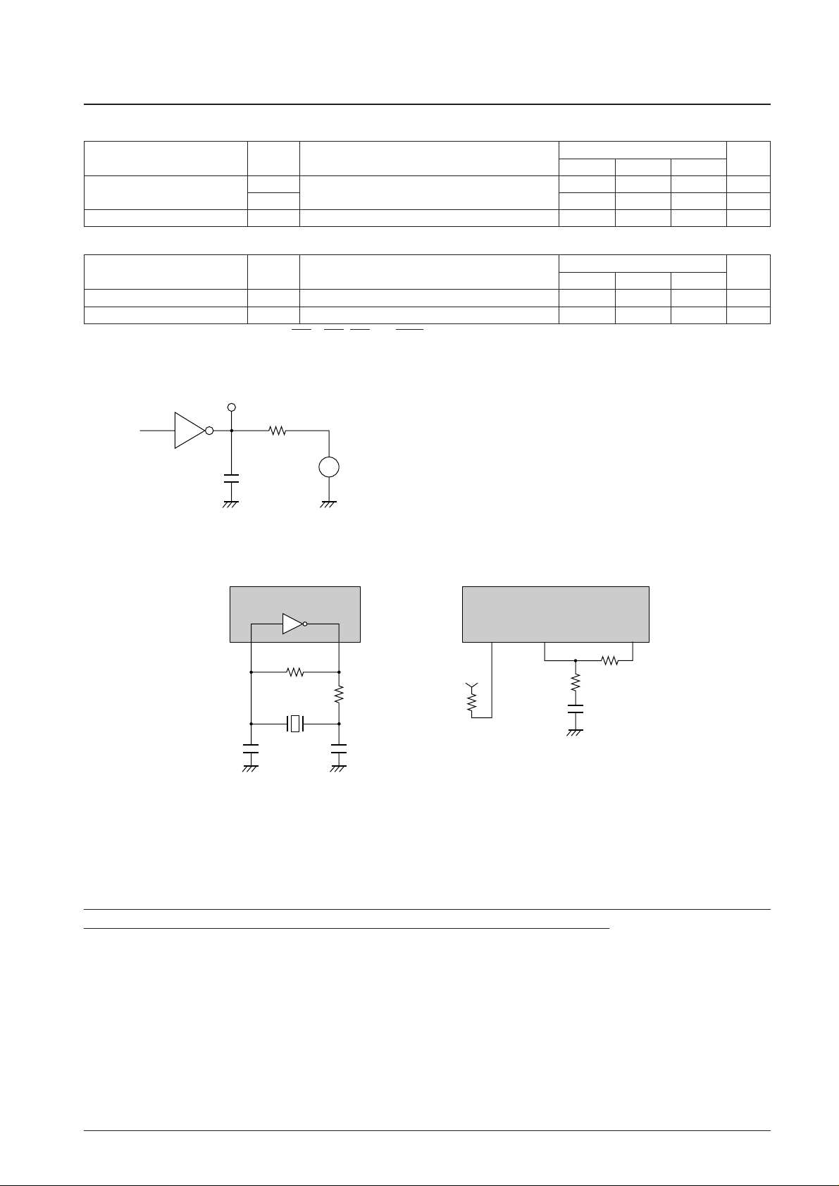
Rise Time Test Circuit
SCSI
Driver
TP
47
Ω±
5%
15pF±5%
2.5V
+
–
A12548
Recommended Oscillator and PLL Circuits
LC897127
R1
R2
C2C1
XTALCK0
PN27
XTAL0
PN28
PN69 PN70 PN71
A12549
LC897127
PLL
R5
R4
C3
R3
A12550
R1 = 120 kΩ, R2 = 47 Ω, C1 = 30 pF
Crystal element oscillator frequency XTALCK0 = 16.9344 MHz
R3 = 7.5 kΩ, R4 = 200 Ω, R5 = 10k Ω, C3 = 0.1 µF
Note: The values listed above for R3, R4, R5, and C3 also apply when the XTALKC0 frequency is 33.8688 MHz.
Applications must be designed so that the analog VDDand VSSpower supply system is completely independent of the
logic system power supply and is not affected by the logic system power supply in any way.
Since the exact values of these components will vary depending on characteristics of the printed circuit board used and
other factors, consult the manufacturer of the crystal element when designing the oscillator circuit.

No. 6251-4/14
LC897127K
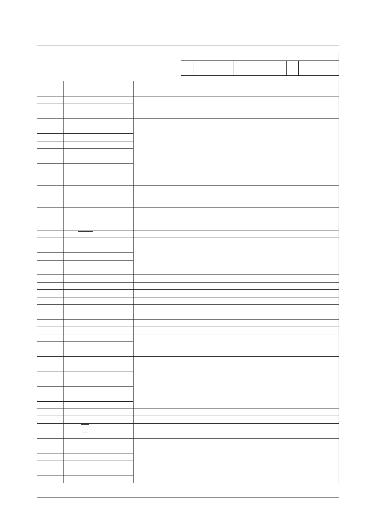
Block Diagram
De-scramble &
Buffering
Address generator
Microcontroller
RAM access
Address generator
Address generator
ECC & EDC
Block
SCSI I/F
Address generator
Data output input I/F
Address generator
CAV-Audio control
Bus
Arbiter
&
RAM
controller
&
IF
controller
DRAM
or
ATAPI
I/F IC
or
DMA
I/F IC
Each Block
Bus control
signal
Each Block
Register
CD-DSP I/F
& SYNC
Detector
CD-DSP
DVD DSP
HOST
Micro
controller
decoder
Clock
generator
&
PLL
*10
*2
*7
DAC
*9
*8
*5
*6
*3
*4
Sub-code I/F
de-interleve
Address generator
DVD DSP I/F
Address generator
*1
EXCK
INT0, 1
SWAIT
XTALCK
XTAL
MCK
Each Block
Data bus[0:7]
Address bus[0:21]
RAM
Data bus[0:15]
LC897127K
A12551
*1. WFCK, SBSO, SCOR
*2. BCK, SDATA, LRCK, C2PO
*3. DB0 to DB7, DBP, BSY, MSG, SEL, RST, REQ, I/O, C/D
*4. ACK, ATN
*5. RD, WR, SUA0 to SUA6, CS, CSCTRL
*6. D0 to D7
*7. IO0 to IO15 (Data bus for both ATAPI and DMA interfaces)
*8. RA0 to RA10, RAS1, RAS0, OE, UWE, LWE
ATAPI interface: SBSO (DMARQ), DBCK (DMACK), DLRCK (DIOR), DSDATA (DIOW)
DMA interface: EXCK (DMARQ), C2PO (DMACK), SDATA (DIOR), BCK (DIOW)
*9. DBCK, DLRCK, DSDATA
*10. HDB7 to HDB0, DRESP, DREQ
See the circuit examples for details on ATAPI and DMA interface IC
connection.
No. 6251-5/14
LC897127K
LC897127K Pin Functions
When the DVD Interface is Used
Type
I INPUT B BIDIRECTION NC NOT CONNECT
O OUTPUT P POWER
Pin No. Pin Type Function
1V
SS0
P
2 IO2 B
Buffer RAM data I/O.
3 IO1 B
These pins have built-in pull-up resistors.
4 IO0 B
5 MCK2SEL I PLL frequency selection. This pin must be connected to V
DD
.
6 C2PO I
7 SDATA I
CD DSP interface
8 BCK I
9 LRCK I
10 EXCK O
Subcode I/O
11 WFCK I
12 SBSO I
Subcode I/O
13 SCOR I
14 DSDATA O
15 DLRCK O D/A converter outputs
16 DBCK O
17 MCK O XTALCLK0 1/1, 1/2, and stop output
18 V
DD
P
19 V
SS0
P
20 RESET I IC reset. The IC is reset on a low-level input.
21 CSCTRL I Microcontroller CS low/high
22 TEST3 I
23 TEST0 I
Test pins. These pins must be connected to V
SS0
in normal operation.
24 TEST1 I
25 TEST2 I
26 V
SS0
P
27 XTALCK0 I Crystal oscillator circuit input
28 XTAL0 O Crystal oscillator circuit output
29 TEST4 I Test pin. This pin must be connected to V
SS0
in normal operation.
30 DRESP B DVD ECC data latching. A pull-down resistor is built in.
31 HDBDIR O DVD data bus direction output. A pull-down resistor is built in.
32 DREQ B DVD ECC data request. A pull-down resistor is built in.
33 V
SS0
P
34 HDB7 I
DVD data input
35 HDB6 I
36 V
SS0
P
37 V
DD
P
38 HDB5 I
39 HDB4 I
40 HDB3 I
DVD data input
41 HDB2 I
42 HDB1 I
43 HDB0 I
44 V
SS0
P
45 RD I Microcontroller data read signal input
46 WR I Microcontroller data write signal input
47 CS I Register chip select input from the microcontroller
48 SUA0 I
49 SUA1 I
50 SUA2 I
Microcontroller register selection signals
51 SUA3 I
52 SUA4 I
53 SUA5 I
Continued on next page.

No. 6251-6/14
LC897127K
Continued from preceding page.
Pin No. Pin Type Function
54 V
DD
P
55 V
SS0
P
56 SUA6 I Microcontroller register selection signals
57 D0 B
58 D1 B
59 D2 B
Microcontroller data signals
60 D3 B
61 D4 B
62 D5 B
63 V
SS0
P
64 D6 B
Microcontroller data signals
65 D7 B
66 INT0 O Interrupt request signal output to the microcontroller (ECC side. Set by setting a register value.)
67 INT1 O Interrupt request signal output to the microcontroller (SCSI side. Set by setting a register value.)
68 SWAIT O Wait signal output to the microcontroller
69 X1EN I Used by the PLL. This pin must be connected to V
DD
through a resistor.
70 XTALCK1 I Used by the PLL.
71 XTAL1 O Used by the PLL.
72 V
SS0
P Analog V
SS
73 V
DD
P Analog V
DD
74 NC
75 I/O B
SCSI interface
76 REQ B
77 V
SS1
P
78 C/D B
SCSI interface
79 SEL B
80 NC
81 V
DD
P
82 V
SS1
P
83 MSG B
SCSI interface
84 RST B
85 V
SS1
P
86 ACK B
SCSI interface
87 BSY B
88 V
SS1
P
89 ATN B SCSI interface
90 V
DD
P
91 V
SS1
P
92 NC
93 DBP B SCSI interface
94 V
DD
P
95 DB7 B
SCSI interface
96 DB6 B
97 V
SS1
P
98 DB5 B
SCSI interface
99 DB4 B
100 V
DD
P
101 DB3 B
SCSI interface
102 DB2 B
103 V
SS1
P
104 DB1 B
SCSI interface
105 DB0 B
106 SCSISEL I SCSI pin layout selection. (This pin must be connected to V
SS0
.)
107 XTALSEL I PLL XATL oscillator selection
Continued on next page.

No. 6251-7/14
LC897127K
Continued from preceding page.
Pin No. Pin Type Function
108 V
SS1
P
109 V
DD
P
110 V
SS0
P
111 RAS0 O Buffer RAM RAS signal output 0
112 DVDSEL P V
SS0
selects the DVD interface and VDDselects the I/O port function.
113 CAS0 O Buffer RAM CAS signal output 0 (Normally fixed at 0 (low).)
114 CAS1 O Buffer RAM CAS signal output 1
115 OE O Buffer RAM output enable
116 UWE(RA9) O Buffer RAM upper write enable (RA9 when 8M or more DRAM is used.)
117 LWE O Buffer RAM lower write enable
118 V
SS0
P
119 RA0 O
120 RA1 O
121 RA2 O
122 RA3 O Buffer RAM address signal outputs
123 RA4 O
124 RA5 O
125 RA6 O
126 V
DD
P
127 V
SS0
P
128 RA7 O
Buffer RAM address signal outputs
129 RA8 O
130 IO15 B
131 IO14 B
132 IO13 B
133 IO12 B Buffer RAM data I/O.
134 IO11 B These pins have built-in pull-up resistors.
135 IO10 B
136 IO9 B
137 IO8 B
138 V
SS0
P
139 IO7 B
140 IO6 B
Buffer RAM data I/O.
141 IO5 B
These pins have built-in pull-up resistors.
142 IO4 B
143 IO3 B
144 V
DD
P
• Unused ("NC") pins must be left open.
• Pins whose name is under a bar operate with inverted (negative) logic.
• V
SS0
is the logic system ground and V
SS1
is the SCSI interface driver ground.
• If DRAM is used, applications must adopt measures to prevent undershoot and other DRAM problems. Such measures include inserting resistors in the
RAS and CAS lines and inserting capacitors between V
SS
pins. See the article on Designing with the Latest Microcontrollers and Memory in special issue
number 25 of Transistor Technology for details on these measures.
• Since this device includes buffers that sink a current of 48 mA, applications must take adequate noise prevention measures.

No. 6251-8/14
LC897127K
LC897127K Pin Functions
When ATAPI to SCSI Conversion is Used
Type
I INPUT B BIDIRECTION NC NOT CONNECT
O OUTPUT P POWER
Pin No. Pin Type Function
1V
SS0
P
2 IO2 B
ATAPI data I/O.
3 IO1 B
These pins have built-in pull-up resistors.
4 IO0 B
5 MCK2SEL I This pin must be connected to V
DD
.
6V
SS0
P
7V
SS0
P
8V
SS0
P
9V
DD
P
10 NC
11 V
DD
P
12 DMARQ I ATAPI interface
13 V
DD
P
14 DIOW O
15 DIOR O ATAPI interface
16 DMACK O
17 MCK O XTALCLK0 1/1, 1/2, and stop output
18 V
DD
P
19 V
SS0
P
20 RESET I IC reset. The IC is reset on a low-level input.
21 CSCTRL I Microcontroller CS low/high
22 TEST3 I
23 TEST0 I
Test pins. These pins must be connected to V
SS0
in normal operation.
24 TEST1 I
25 TEST2 I
26 V
SS0
P
27 XTALCK0 I Crystal oscillator circuit input
28 XTAL0 O Crystal oscillator circuit output
29 TEST4 I Test pin. This pin must be connected to V
SS0
in normal operation.
30 V
SS0
P
31 V
SS0
P
32 V
SS0
P
33 V
SS0
P
34 IOP7 I General-purpose inputs
35 IOP6 I These pins have built-in pull-up resistors.
36 V
SS0
P
37 V
DD
P
38 IOP5 I
39 IOP4 I
40 IOP3 I General-purpose inputs
41 IOP2 I These pins have built-in pull-up resistors.
42 IOP1 I
43 IOP0 I
44 V
SS0
P
45 RD I Microcontroller data read signal input
46 WR I Microcontroller data write signal input
47 CS I Register chip select input from the microcontroller
48 SUA0 I
49 SUA1 I
50 SUA2 I
Microcontroller register selection signals
51 SUA3 I
52 SUA4 I
53 SUA5 I
Continued on next page.

No. 6251-9/14
LC897127K
Continued from preceding page.
Pin No. Pin Type Function
54 V
DD
P
55 V
SS0
P
56 SUA6 I Microcontroller register selection signals
57 D0 B
58 D1 B
59 D2 B
Microcontroller data signals
60 D3 B
61 D4 B
62 D5 B
63 V
SS0
P
64 D6 B
Microcontroller data signals
65 D7 B
66 INT0 O Interrupt request signal output to the microcontroller (ECC side. Set by setting a register value.)
67 INT1 O Interrupt request signal output to the microcontroller (SCSI side. Set by setting a register value.)
68 SWAIT O Wait signal output to the microcontroller
69 X1EN I Used by the PLL. This pin must be connected to V
DD
through a resistor.
70 XTALCK1 I Used by the PLL.
71 XTAL1 O Used by the PLL.
72 V
SS0
P Analog V
SS
73 V
DD
P Analog V
DD
74 NC
75 I/O B
SCSI interface
76 REQ B
77 V
SS1
P
78 C/D B
SCSI interface
79 SEL B
80 NC
81 V
DD
P
82 V
SS1
P
83 MSG B
SCSI interface
84 RST B
85 V
SS1
P
86 ACK B
SCSI interface
87 BSY B
88 V
SS1
P
89 ATN B SCSI interface
90 V
DD
P
91 V
SS1
P
92 NC
93 DBP B SCSI interface
94 V
DD
P
95 DB7 B
SCSI interface
96 DB6 B
97 V
SS1
P
98 DB5 B
SCSI interface
99 DB4 B
100 V
DD
P
101 DB3 B
SCSI interface
102 DB2 B
103 V
SS1
P
104 DB1 B
SCSI interface
105 DB0 B
106 SCSISEL I SCSI pin layout selection. (This pin must be connected to V
SS0
.)
107 XTALSEL I PLL XATL oscillator selection
Continued on next page.

No. 6251-10/14
LC897127K
Continued from preceding page.
Pin No. Pin Type Function
108 V
SS1
P
109 V
DD
P
110 V
SS0
P
111 NC
112 V
DD
P
113 NC
114 NC
115 NC
116 NC
117 NC
118 V
SS0
P
119 NC
120 NC
121 NC
122 NC
123 NC
124 NC
125 NC
126 V
DD
P
127 V
SS0
P
128 NC
129 NC
130 IO15 B
131 IO14 B
132 IO13 B
133 IO12 B ATAPI data I/O
134 IO11 B These pins have built-in pull-up resistors.
135 IO10 B
136 IO9 B
137 IO8 B
138 V
SS0
P
139 IO7 B
140 IO6 B
ATAPI data I/O
141 IO5 B
These pins have built-in pull-up resistors.
142 IO4 B
143 IO3 B
144 V
DD
P
• Unused ("NC") pins must be left open.
• Pins whose name is under a bar operate with inverted (negative) logic.
• V
SS0
is the logic system ground and V
SS1
is the SCSI interface driver ground.
• Since this device includes buffers that sink a current of 48 mA, applications must take adequate noise prevention measures.

No. 6251-11/14
LC897127K
LC897127K Pin Functions
When DMA Interface to SCSI Conversion is Used
Type
I INPUT B BIDIRECTION NC NOT CONNECT
O OUTPUT P POWER
Pin No. Pin Type Function
1V
SS0
P
2 IO2 B
DAM interface data I/O.
3 IO1 B
These pins have built-in pull-up resistors.
4 IO0 B
5 MCK2SEL I This pin must be connected to V
DD
.
6 DMACK I
7 DIOR I DMA interface functions
8 DIOW I
9V
DD
P
10 DMARQ O DMA interface functions
11 V
DD
P
12 V
DD
P
13 V
DD
P
14 NC
15 NC
16 NC
17 MCK O XTALCLK0 1/1, 1/2, and stop output
18 V
DD
P
19 V
SS0
P
20 RESET I IC reset. The IC is reset on a low-level input.
21 CSCTRL I Microcontroller CS low/high
22 TEST3 I
23 TEST0 I
Test pins. These pins must be connected to V
SS0
in normal operation.
24 TEST1 I
25 TEST2 I
26 V
SS0
P
27 XTALCK0 I Crystal oscillator circuit input
28 XTAL0 O Crystal oscillator circuit output
29 TEST4 I Test pin. This pin must be connected to V
SS0
in normal operation.
30 V
SS0
P
31 V
SS0
P
32 V
SS0
P
33 V
SS0
P
34 IOP7 I General-purpose inputs
35 IOP6 I These pins have built-in pull-up resistors.
36 V
SS0
P
37 V
DD
P
38 IOP5 I
39 IOP4 I
40 IOP3 I General-purpose inputs
41 IOP2 I These pins have built-in pull-up resistors.
42 IOP1 I
43 IOP0 I
44 V
SS0
P
45 RD I Microcontroller data read signal input
46 WR I Microcontroller data write signal input
47 CS I Register chip select input from the microcontroller
48 SUA0 I
49 SUA1 I
50 SUA2 I
Microcontroller register selection signals
51 SUA3 I
52 SUA4 I
53 SUA5 I
Continued on next page.

No. 6251-12/14
LC897127K
Continued from preceding page.
Pin No. Pin Type Function
54 V
DD
P
55 V
SS0
P
56 SUA6 I Microcontroller register selection signals
57 D0 B
58 D1 B
59 D2 B
Microcontroller data signals
60 D3 B
61 D4 B
62 D5 B
63 V
SS0
P
64 D6 B
Microcontroller data signals
65 D7 B
66 INT0 O Interrupt request signal output to the microcontroller (ECC side. Set by setting a register value.)
67 INT1 O Interrupt request signal output to the microcontroller (SCSI side. Set by setting a register value.)
68 SWAIT O Wait signal output to the microcontroller
69 X1EN I Used by the PLL. This pin must be connected to V
DD
through a resistor.
70 XTALCK1 I Used by the PLL.
71 XTAL1 O Used by the PLL.
72 V
SS0
P Analog V
SS
73 V
DD
P Analog V
DD
74 NC
75 I/O B
SCSI interface
76 REQ B
77 V
SS1
P
78 C/D B
SCSI interface
79 SEL B
80 NC
81 V
DD
P
82 V
SS1
P
83 MSG B
SCSI interface
84 RST B
85 V
SS1
P
86 ACK B
SCSI interface
87 BSY B
88 V
SS1
P
89 ATN B SCSI interface
90 V
DD
P
91 V
SS1
P
92 NC
93 DBP B SCSI interface
94 V
DD
P
95 DB7 B
SCSI interface
96 DB6 B
97 V
SS1
P
98 DB5 B
SCSI interface
99 DB4 B
100 V
DD
P
101 DB3 B
SCSI interface
102 DB2 B
103 V
SS1
P
104 DB1 B
SCSI interface
105 DB0 B
106 SCSISEL I SCSI pin layout selection. (This pin must be connected to V
SS0
.)
107 XTALSEL I PLL XATL oscillator selection
Continued on next page.

No. 6251-13/14
LC897127K
Continued from preceding page.
Pin No. Pin Type Function
108 V
SS1
P
109 V
DD
P
110 V
SS0
P
111 NC
112 V
DD
P
113 NC
114 NC
115 NC
116 NC
117 NC
118 V
SS0
P
119 NC
120 NC
121 NC
122 NC
123 NC
124 NC
125 NC
126 V
DD
P
127 V
SS0
P
128 NC
129 NC
130 IO15 B
131 IO14 B
132 IO13 B
133 IO12 B DMA interface data I/O.
134 IO11 B These pins have built-in pull-up resistors.
135 IO10 B
136 IO9 B
137 IO8 B
138 V
SS0
P
139 IO7 B
140 IO6 B
ATAPI data I/O.
141 IO5 B
These pins have built-in pull-up resistors.
142 IO4 B
143 IO3 B
144 V
DD
P
• Unused ("NC") pins must be left open.
• Pins whose name is under a bar operate with inverted (negative) logic.
• V
SS0
is the logic system ground and V
SS1
is the SCSI interface driver ground.
• Since this device includes buffers that sink a current of 48 mA, applications must take adequate noise prevention measures.

PS No. 6251-14/14
LC897127K
This catalog provides information as of November, 1999. Specifications and information herein are
subject to change without notice.
Specifications of any and all SANYO products described or contained herein stipulate the performance,
characteristics, and functions of the described products in the independent state, and are not guarantees
of the performance, characteristics, and functions of the described products as mounted in the customer’s
products or equipment. To verify symptoms and states that cannot be evaluated in an independent device,
the customer should always evaluate and test devices mounted in the customer’s products or equipment.
SANYO Electric Co., Ltd. strives to supply high-quality high-reliability products. However, any and all
semiconductor products fail with some probability. It is possible that these probabilistic failures could
give rise to accidents or events that could endanger human lives, that could give rise to smoke or fire,
or that could cause damage to other property. When designing equipment, adopt safety measures so
that these kinds of accidents or events cannot occur. Such measures include but are not limited to protective
circuits and error prevention circuits for safe design, redundant design, and structural design.
In the event that any or all SANYO products (including technical data, services) described or contained
herein are controlled under any of applicable local export control laws and regulations, such products must
not be exported without obtaining the export license from the authorities concerned in accordance with the
above law.
No part of this publication may be reproduced or transmitted in any form or by any means, electronic or
mechanical, including photocopying and recording, or any information storage or retrieval system,
or otherwise, without the prior written permission of SANYO Electric Co., Ltd.
Any and all information described or contained herein are subject to change without notice due to
product/technology improvement, etc. When designing equipment, refer to the “Delivery Specification”
for the SANYO product that you intend to use.
Information (including circuit diagrams and circuit parameters) herein is for example only; it is not
guaranteed for volume production. SANYO believes information herein is accurate and reliable, but
no guarantees are made or implied regarding its use or any infringements of intellectual property rights
or other rights of third parties.
 Loading...