

SANYO LC895925 Datasheet
Overview
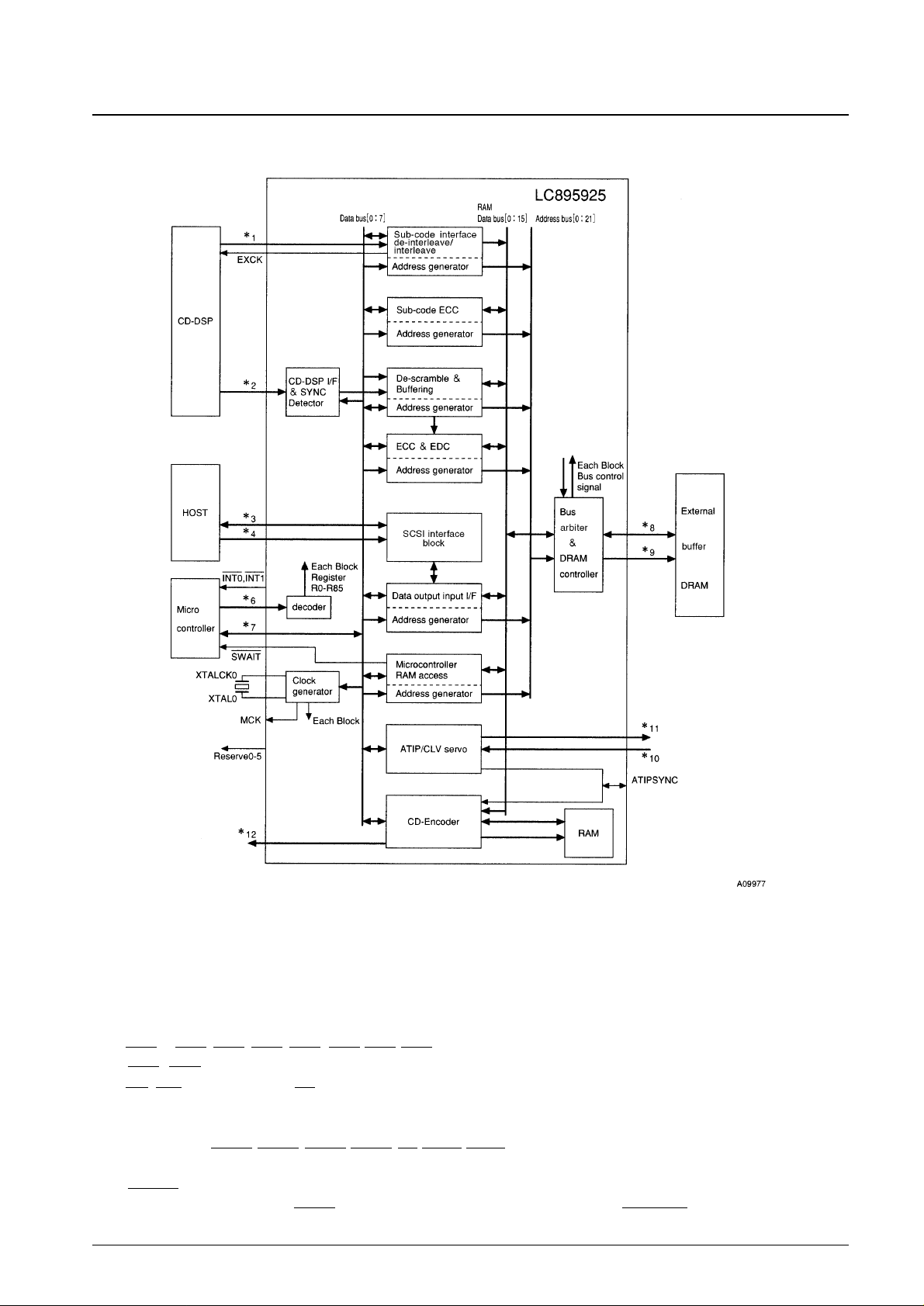
The LC895925 provides the following signal processing
functions for CD-R drives: CD-ROM decoding/encoding
(complete with ECC processing for the former), subcode
decoding/encoding, CD encoding, ATIP decoding, CLV
servo, and SCSI interface registers.
Features
• CD-ROM decoding/encoding complete with error
detection and error correction
• Subcode decoding/encoding complete with error
correction
• ATIP decoding and CRC checking for both encoding
and decoding
• CLV servo control using ATIP data during encoding
• CIRC code insertion and EFM modulation during
encoding
• Support for PCA random EFM output during encoding
• Support for CD-ReWritable (CD-RW) Write Strategy
signal output
• Access to buffer RAM from microcontroller via
LC895925
• Built-in SCSI interface
• Speeds of 12× for decoding and 4× for encoding
— Frequencies
Decoding: 17.2872 MHz
Encoding: 17.2872 MHz without Write Strategy
support
69.1488 MHz with Write Strategy
support
• Transfers speeds of 10 megabytes/s (synchronous) and 5
megabytes/s (asynchronous) with 16 80-ns DRAMs *1
• Buffer RAM sizes between 1 and 32 megabits (using 16bit DRAMs)
• User control over sizes of CD main channel, C2 flag,
and subcode areas in buffer RAM
• Built-in batch transfer function for transferring entire
CD main channel, C2 flag, or subcode area in a single
operation
• Built-in multiblock transfer function for transferring
multiple blocks in a single operation
Notes:
1. Using a SCSI master clock of 20 MHz with speeds up
to 8×.
2. Using a SCSI master clock of 17.2872 MHz with
speeds up to 4×.
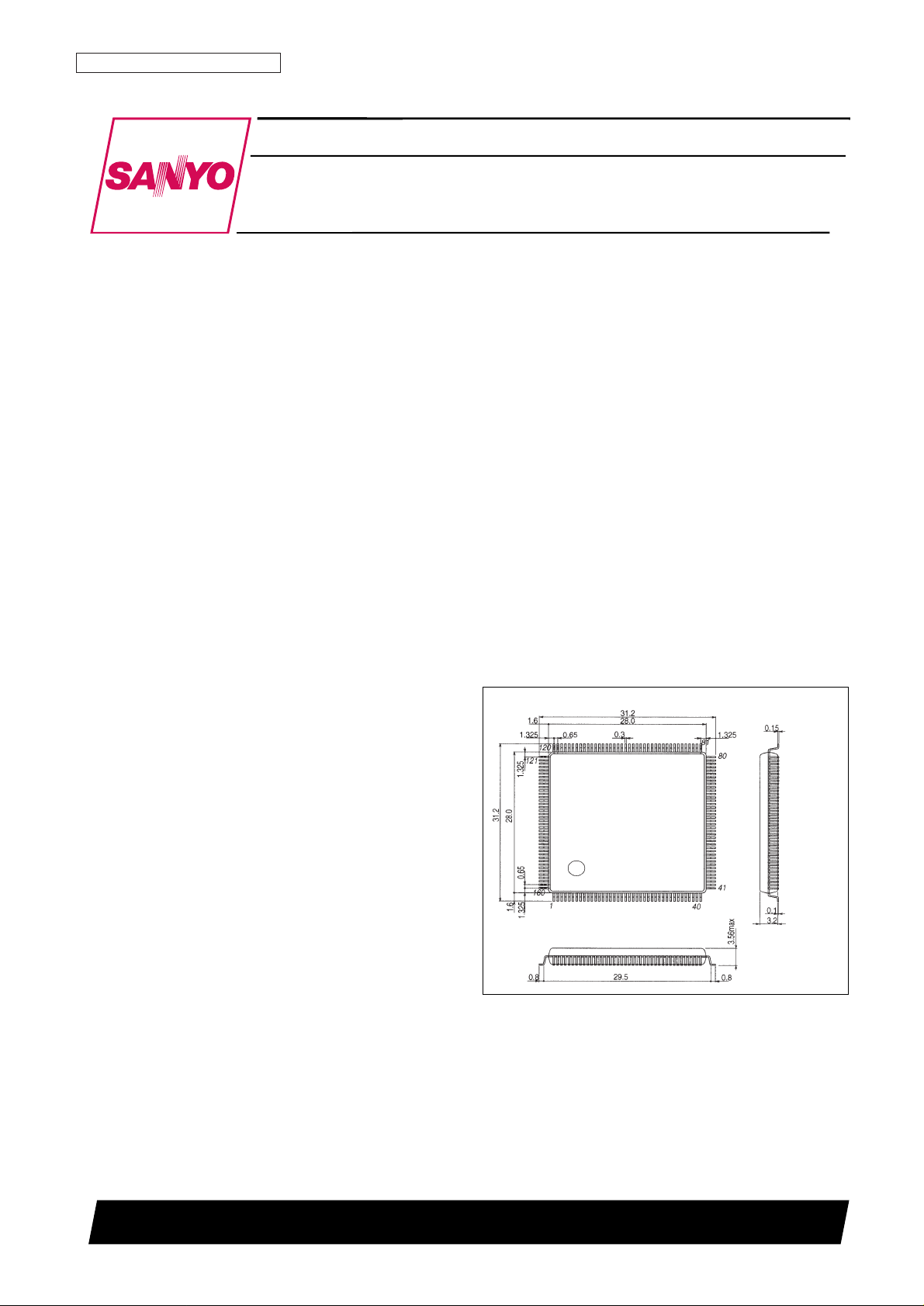
Package Dimensions
unit: mm
3153A-QFP160E
CMOS LSI
D1997RM (OT) No. 5784-1/7
Preliminaly
SANYO: QIP160E
[LC895925]
SANYO Electric Co.,Ltd. Semiconductor Bussiness Headquarters
TOKYO OFFICE Tokyo Bldg., 1-10, 1 Chome, Ueno, Taito-ku, TOKYO, 110-0005 JAPAN
Signal Processing LSI for CD-R Drives
LC895925
Ordering number : EN*5784
No. 5784-2/7
LC895925
Parameter Symbol Conditions Ratings Unit
Maximum power supply voltage V
DD
max –0.3 to +7.0 V
I/O voltage V
I
, V
O
–0.3 to VDD+0.3 V
Maximum power dissipation Pd max Ta ≤ 70°C 600 mW
Operating temperature Topr –30 to +70 °C
Storage temperature Tstg –55 to +125 °C
Solder resistance 10 seconds 260 °C
Specifications
Maximum Ratings at Ta = 25°C, VSS= 0 V
Parameter Symbol Conditions
Ratings
Unit
min typ max
Input high level voltage V
IH
TTL levels, for pin types 1 and 6
2.2 V
Input low level voltage V
IL
0.8 V
Input high level voltage V
IH
TTL levels, for pin type 4, with pull-up resistors
2.2 V
Input low level voltage V
IL
0.8 V
Input high” level voltage V
IH
TTL levels, for pin 0 and 7, with Schmitt inputs
2.5 V
Input low level voltage V
IL
0.6 V
Output high level voltage V
OHIOH
= –2 mA, for pin type 3 VDD– 2.1 V
Output low level voltage V
OLIOL
= 2 mA, for pin type 3 0.4 V
Output high level voltage V
OHIOH
= -2 mA, for pin types 2, 4, and 6 VDD– 2.1 V
Output low level voltage V
OLIOL
= 2 mA, for pin types 2, 4, and 6 0.4 V
Output high level voltage V
OHIOH
= -48 mA, for pin type 7 VDD– 2.1 V
Output low level voltage V
OLIOL
= 48 mA, for pin type 7 0.4 V
Output low level voltage V
OLIOL
= 2 mA, for pin type 5 0.4 V
Input leak current I
IL
VI= VSS, VDD, for pin types 0, 1, 6, and 7 –10 +10 µA
Pull-up resistance R
UP
For pin types 4 and 5 40 80 160 kΩ
DC Characteristics at Ta = –30 to +70°C, VSS= 0 V, VDD= 4.5 to 5.5 V
Parameter Symbol Conditions
Ratings
Unit
min typ max
Supply voltage V
DD
4.5 5.0 5.5 V
Input voltage range V
IN
0 V
DD
V
Permissible Operating Range at Ta = –30 to +70°C, VSS= 0 V
The pin types above refer to the following groups.
Input
(0) BCK, BICLKIN, BIDATAI, C2PO, LOCKIN, LRCK, PLLOUTIN, ROUGH, SBSO, SCOR, SDATA, WFCK, CS,
RD, WR
(1) SUA0 to SUA6, TEST0 to TEST6, X1EN, RESET
Output
(2) CLV+, CLV–, FSW
(3) DATACKO, EFM, EFMG, EFMGATE0 to EFMGATE6, EXCK, LOCK, MCK, MON, PSUBSYNC, RA0 to RA9,
SUBSYNC, CAS0 to CAS1, RAS0 to RAS1, ERROR, EXTACK, FRCK, LWE, UWE, OE
Input/Output
(4) D0 to D7, IO0 to IO15
(5) INT0 to INT1, SWAIT
(6) ATIPSYNC, Reserve0 to Reserve5
(7) ACK, ATN, BSY, C/D, DB0 to DB7, DBP, I/O, MSG, REQ, RST, SEL
Note: The XTAL0, XTAL1, XTALCK0, and XTALCK1 pins fall outside of these DC characteristic specifications.
*1 WFCK, SBSO, SCOR
*2 BCK, SDATA, LRCK, C2PO
*3 DB0 to DB7, DBP, BSY, MSG, SEL, RST, REQ, I/O, C/D
*4 ACK, ATN
*6 RD, WR, SUA0 to SUA6, CS
*7 D0 to D7
*8 IO0 to IO15
*9 RA0 to RA9, RAS0, RAS1, CAS0, CAS1, OE, UWE, LWE
*10 PLLOUTIN, ROUGH, LOCKIN, BICLKIN, BIDATAIN
*11 ERROR, LOCK, CLV+(MDP), CLV–(MDS), MON, FSW
*12 SUBSYNC, PSUBSYNC, FRCK, EFM, EFMG, EFMGATE3 to EFMGATE0, EXTACK, DATACK0
Block Diagram
No. 5784-3/7
LC895925
 Loading...