

Page 1
Any and all SANYO products described or contained herein do not have specifications that can handle
applications that require extremely high levels of reliability, such as life-support systems, aircraft’s
control systems, or other applications whose failure can be reasonably expected to result in serious
physical and/or material damage. Consult with your SANYO representative nearest you before using
any SANYO products described or contained herein in such applications.
SANYO assumes no responsibility for equipment failures that result from using products at values that
exceed, even momentarily, rated values (such as maximum ratings, operating condition ranges,or other
parameters) listed in products specifications of any and all SANYO products described or contained
herein.
CMOS IC
General-Purpose 68000 MPU
Peripheral Interface IC
Ordering number:ENN3411B
LC8953
SANYO Electric Co.,Ltd. Semiconductor Company
TOKYO OFFICE Tokyo Bldg., 1-10, 1 Chome, Ueno, Taito-ku, TOKYO, 110-8534 JAPAN
PUPPET (Programmable Universal Peripheral/Port Expansion uniT)
Overview
There are many application systems using the 68000 chip
as their MPU (Main Processing Unit). It is common to them
that designing the peripheral circuits such as address decoders, interrupt controllers, serial interface and DMA (Direct Memory Access) has become a time-consuming task.
As a result, each of the application systems requires a larger
board size, which makes it very expensive.
In addition, 68000 family peripherals are highly advanced
functional ICs. The application system designer finds it difficult to use them in small- and medium-sized application
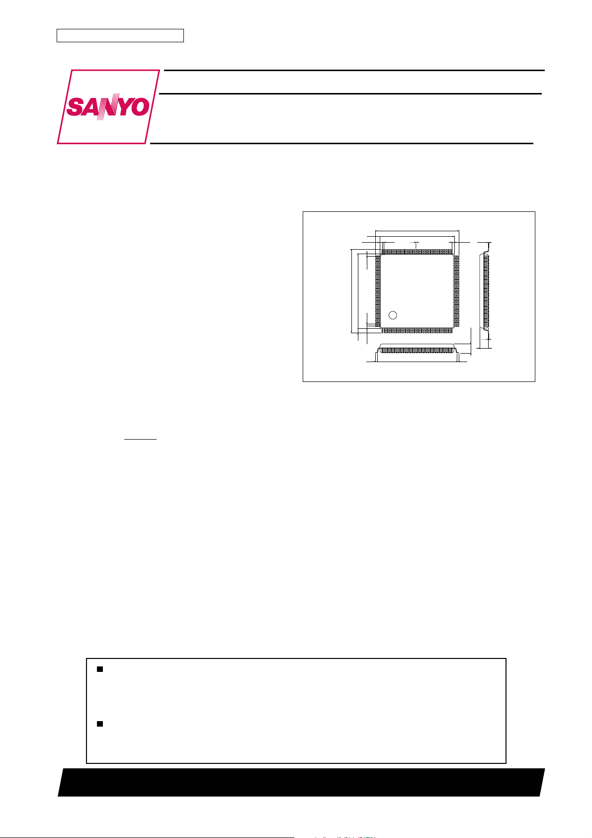
Package Dimensions
unit:mm
3153A-QIP160E
[LC8953]
1.6
1.325
121
1.325
31.2
28.0
31.2
28.0
0.3
0.65
120
81
products in terms of cost as well as functional complexity.
The LC8953 (Programmable Universal Peripheral/Port
Expansion uniT) has optimized on-chip control circuits
enabling the 68000 MPU to control the LC8951 (RCHIP)
and LC8955. Use of the optimized control circuits allows
0.65
160
140
1.6
1.325
0.8
29.5
the user to easily build up CD-ROM and CD-I systems
which offer excellent performance in terms of space and
cost.
Features
• Programmable address decoder.
• Programmable DTACK generator.
• Programmable interrupt handler.
• Clock divider.
• Bus error generator.
• TICK generator (programmable timer interrupt generator)
• Serial mouse interface (1 port)
• LC8951 (RCHIP–Real-time error Correction & Host-interface Integrated Processor) interface.
• LC8955 interface.
• Micro-programmable 1-channel DMA controller.
1.325
0.15
80
41
0.1
3.56max
3.2
0.8
SANYO : QIP160E
80101TN (KT)/D1394TH (ID)/N010JNKI No.3411–1/9
Page 2
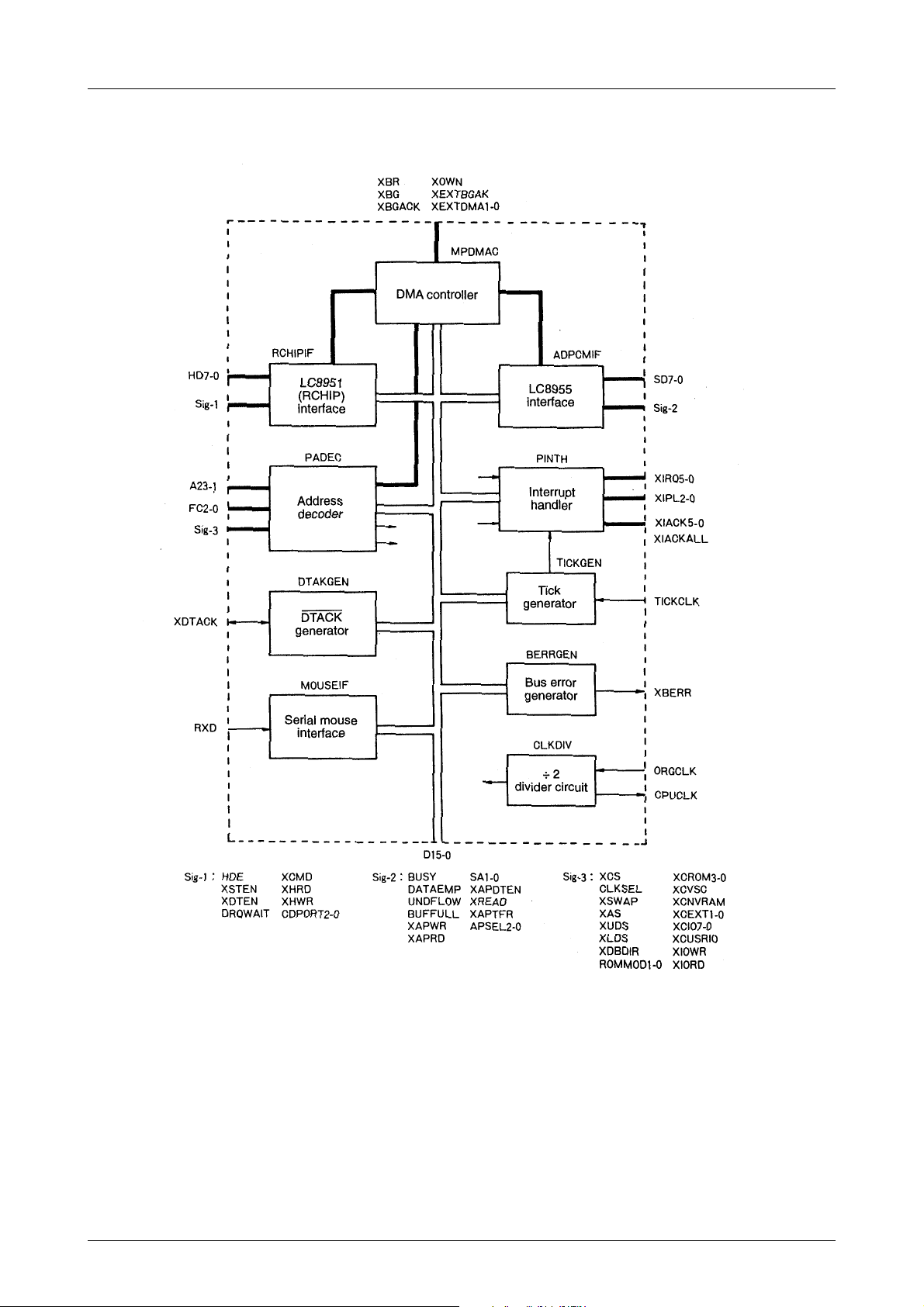
Block Diagram
LC8953
No.3411–2/9
Page 3
Pin Assignment
LC8953
No.3411–3/9
Page 4

Pin Functions
rebmuNemaN
1VSS–nipdnuorG
2PMEATADI 5598CLehtrofniptupnilangisytpmeataD
3WOLFDNUI 5598CLehtrofniptupnilangiswolfrednU
4LLUFFUBI 5598CLehtrofniptupnilangisllufreffuB
5YSUBI 5598CLehtrofniptupnilangisysuB
6RWPAXI 5598CLehtrofniptupnilangisetirwataD
7DRPAXI 5598CLehtrofniptupnilangisdaerataD
8SCPAXI 5598CLehtrofniptupnitcelespihC
90ASO
011ASO
110DSO/I
211DSO/I
312DSO/I
413DSO/I
514DSO/I
615DSO/I
716DSO/I
817DSO/I
91NETDPAXO refsnarttseuqercitamotuarof5598CLehtrofniptuptuolangiselbaneataD
02VDD–nipylppusV5+
12VSS–nipdnuorG
22DAERXI refsnarttseuqercitamotuarof5598CLehtrofniptupnilangisdaeR
32TSETI )woldeiT(niptupnitseT
420DHO/I
521DHO/I
622DHO/I
723DHO/I
824DHO/I
925DHO/I
036DHO/I
137DHO/I
23EDHI )PIHCR(1598CLehtrofniptupnilangisgalferusarE
33NETSXI )PIHCR(1598CLehtrofniptupnilangiselbanesutatS
43NETDXI )PIHCR(1598CLehtrofniptupnilangiselbaneataD
53TIAWQRDI )PIHCR(1598CLehtrofniptupnilangistcelestiaW/tseuqerataD
63DMCXO )PIHCR(1598CLehtrofniptuptuolangistcelesataD/dnammoC
73DRHXO )PIHCR(1598CLehtrofniptuptuolangisdaerataD
83RWHXO )PIHCR(1598CLehtrofniptuptuolangisetirwataD
930TROPDCO/Iniplangistuptuo/tupniesoprup-lareneG
04VDD–nipylppusV5+
14VSS–nipdnuorG
241TROPDCO/I
342TROPDCO/I
44RFTPAXI refsnarttseuqercitamotua5598CLehtrofniptupnilangistcelesnoitarepoksaM
54DROIXO sCIlarehpirepletnIrofniptuptuolangisdaerCI
64RWOIXO sCIlarehpirepletnIrofniptuptuolangisetirW
74OIRSUCXO niptuptuolangistcelessserddaO/IresU
840OICXO
941OICXO
052OICXO
153OICXO
254OICXO
355OICXO
456OICXO
557OICXO
650TXECXO
751TXECXO
85MARVNCXO niptuptuolangistcelessserddaMARVN
95CSVCXO niptuptuolangistcelessserddaCSV
1
O/InoitcnuF
LC8953
5598CLehtrofsniptuptuolangistcelesretsiseR
5598CLehtrofsnipO/IlangisataD
)PIHCR(1598CLehtrofsnipO/IlangisataD
sniplangistuptuo/tupniesoprup-lareneG
sniptuptuolangistcelessserddaO/IelbammargorP
sniptuptuolangistcelessserddalanretxE
Continued on next page.
No.3411–4/9
Page 5

Continued from preceding page.
rebmuNemaN
06VDD–nipylppusV5+
16VSS–nipdnuorG
260MORCXO
361MORCXO
462MORCXO
563MORCXO
661DOMMORI
760DOMMORI
86KCATDXO/Iniptuptuo/tupnilangisegdelwonkcaataD
96WRXO/Iniptuptuo/tupnilangisetirW/daeR
07SDLXO/Iniptuptuo/tupnilangisebortsatadredro-woL
17SDUXO/Iniptuptuo/tupnilangisebortsatadredro-hgiH
27SAXO/Iniptuptuo/tupnilangisebortssserddA
370DO/I
471DO/I
572DO/I
673DO/I
774DO/I
875DO/I
976DO/I
087DO/I
18VSS–nipdnuorG
288DO/I
389DO/I
4801DO/I
5811DO/I
6821DO/I
7831DO/I
8841DO/I
9851DO/I
09VDD–nipylppusV5+
1932AO/I
2922AO/I
3912AO/I
4902AO/I
5991AO/I
6981AO/I
7971AO/I
8961AO/I
99VSS–nipdnuorG
00151AO/I
10141AO/I
20131AO/I
30121AO/I
40111AO/I
50101AO/I
6019AO/I
701VDD–nipylppusV5+
8018AO/I
9017AO/I
0116AO/I
1115AO/I
2114AO/I
3113AO/I
4112AO/I
5111AO/I
611VSS–nipdnuorG
7112LPIXO
9110LPIXO
1
O/InoitcnuF
LC8953
sniptuptuolangistcelessserddaMOR
sniptupnilangistcelesedomMOR
sniptuptuo/tupnilangissubataD
sniptuptuo/tupnilangissubataD
sniptuptuo/tupnilangissubsserddA
sniptuptuo/tupnilangissubsserddA
sniptuptuo/tupnilangissubsserddA
UPMehtrofsniptuptuolangisleveltpurretnI8111LPIXO
Continued on next page.
No.3411–5/9
Page 6

Continued from preceding page.
rebmuNemaN
021VDD–nipylppusV5+
1210CFO/I
3212CFO/I
421RREBXO niptuptuolangisrorresuB
521TESERXI niptupnilangisteseR
621TLAHXI niptupnilangistlaH
721KLCUPCO niptuptuolangiskcolcUPM
821RIDBDXO niptuptuolangisnoitceridsubataD
921RBXO niptuptuolangistseuqersubAMD
031GBXI niptupnilangisdetnarg-tseuqersubAMD
131KCAGBXO niptuptuolangisegdelwonkcadetnarg-tseuqersubAMD
231NWOXO niptuptuolangisevitcaelcycAMD
3311AMDTXEXO/I
4310AMDTXEXO/I
531KAGBTXEXI niptupnilangisegdelwonkcadetnarg-tseuqersubAMDlanretxE
631SCXI niptupnilangistcelesedomredocedsserddA
731LESKLCI niptupnilangistcelesredivid)KLCUPC(kcolcretsaM
831PAWSXI niptupnilangistcelesnoitcnufpawsyromeM
931KLCGROI niptupnikcolC
041VDD–nipylppusV5+
141VSS–nipdnuorG
241KLCKCITI rotarenegkcitehtrofniptupnikcolclanretxE
341LLAKCAIXO niptuptuolangisnommocegdelwonkcatpurretnI
4415KCAIXO
5414KCAIXO
6413KCAIXO
7412KCAIXO
8411KCAIXO
9410KCAIXO
0515QRIXI
1514QRIXI
2513QRIXI
3512QRIXI
4511QRIXI
5510QRIXI
651DXRI niptupnilangisatadesuoM
7510LESPAO
9512LESPAO
061VDD–nipylppusV5+
1
LC8953
O/InoitcnuF
sniptuptuo/tupnilangisedocnoitcnufUPM2211CFO/I
sniptuptuo/tupnilangisAMD
sniptuptuolangisegdelwonkcatpurretnI
sniptupnilangistseuqertpurretnI
sniptroptuptuoesoprup-lareneG8511LESPAO
1. An “X” at the beginning of a pin name indicates negative logic.
No.3411–6/9
Page 7

LC8953
Specifications
Absolute Maximum Ratings at VSS = 0V
retemaraPlobmySsnoitidnoCsgnitaRtinU
egatlovylppusmumixaMV
egatlovtuptuodnatupnIV
noitapissidrewopelbawollAxamdPaT ≤ 07°C 004Wm
egnarerutarepmetgnitarepOrpoT –07+ot03
egnarerutarepmetegarotSgtsT –521+ot55
erutarepmetgniredloSlosT
Allowable Operating Ranges at Ta = –30 to +70˚C, VSS = 0V
retemaraPlobmySsnoitidnoC
egatlovylppuSV
egnaregatlovtupnIV
DC Electrical Characteristics at Ta = –30 to +70˚C, VSS = 0V, VDD = 4.5 to 5.5V
retemaraPlobmySsnoitidnoC
egatlovlevel-hgihtupnIV
egatlovleve-woltupnIV
egatlovlevel-hgihtupnIV
egatlovlevel-woltupnIV
egatlovlevel-hgihtuptuOV
egatlovlevel-woluptuOV
tnerrucegakaeltupnII
tnerrucegakaeltuptuOI
egatlovlevel-hgihtupnIV
egatlovlevel-woltupnIV
egatlovlevel-hgihtuptuOV
egatlovlevel-woluptuOV
xam52=aT°C – 0.7+ot3.0V
DD
IV,O
DD
NI
1
HI
1 8.0V
LI
2
HI
2 6.0V
LI
1IHO=– Am3
HO
1ILOAm3= 4.0V
LO
L
ZO
3
HI
3 V3.0
LI
2IHO=– Am6
HO
2ILOAm6= 4.0V
LO
52=aT°C –ot3.0VDD3.0+V
s3,gniredloslaunaM 053
s01,gniredloswolfeR 532
gnidulcni(sniptupnillA:elbitapmocLTT
setonnidetsilesohttpecxe)sniplanoitceridib
.1etoneeS:ttimhcSelbitapmoc-LTT
esohttpecxesniptupnillA
sniplanoitceridibllA
)931nip(KLCGRO:elbitapmocSOMC
VIV=SSV,
.2dna1
.3etonnidetsil
DD
-nadepmi-hgiH
tuptuoec
)98ot37snip(
nimpytxam
5.40.55.5V
0V
nimpytxam
2.2V
5.2V
4.2V
–5252+Aµ
–001001+Aµ
V7.0
DD
51Dot0D,)86nip(KCATDX
4.2V
˚C
˚C
˚C
˚C
sgnitaR
sgnitaR
tinU
V
DD
tinU
V
V
DD
Notes
1. DATAEMP (pin 2), UNDFLOW (pin 3), BUFFULL (pin 4), BUSY (pin 5), XSTEN (pin 33), XDTEN (pin 34),
DRQWAIT (pin 35), XAPTFR (pin 44), XRESET (pin 125), XHALT (pin 126), XEXTBGAK (pin 135), XIRQ0 to 5
(pins 150 to 155), RXD (pin 156)
2. ORGCLK (pin 139)
3. XDTACK (pin 68), D0 to D15 (pins 73 to 89)
No.3411–7/9
Page 8

LC8953
Internal Functional Blocks
The PUPPET consists of about 10 functional blocks. See
the “Block Diagram”.
PADEC (Programmable Address Decoder)
The PADEC functional block is used to generate the chip
select (CS) signals for ROM, RAM, I/O devices and so on.
The CS signal addresses are programmable, which enables
address allocation specific to your system configuration.
DTAKGEN (Programmable DTACK Generator)
The DTAKGEN functional block is used to generate the
data acknowledge signals for the chip select address space
selected by the PADEC. The access speed of peripheral IC
devices is generally slower than that of the main processing unit (MPU). To adjust this speed gap between them,
the user is allowed to insert from 0 to 4 wait cycles into
each address cycle. The number of wait cycles to be inserted is programmable. In addition, the user is permitted
to disable the DTACK (activ e low) generator so that it can
be generated by an external device.
PINTH (Programmable Interrupt Handler)
The PINTH functional block is used as an interrupt handler to output the vectored numbers corresponding to the
68000 MPU vectored interrupts. Each of the IPL levels and
vectored numbers for internal block/external interrupt requests is programmable.
RCHIPIF (LC8951 RCHIP Interface)
The RCHIPIF functional block is used to provide the interface between the 68000 MPU and the LC8951 RCHIP. This
interface enables direct communication between them. As
a result, status data, data signal and error bit information
can be directly communicated between them.
ADPCMIF (LC8955 Interface)
The ADPCMIF functional block is used to provide the interface between the 68000 MPU and the LC8955. This interface enables direct communication between them. As a
result, data can be directly read from or written to internal
registers of the LC8955 from the MPU.
TICKGEN (Tick Generator)
The TICKGEN functional block is used to generate timer
interrupt clocks for a real-time operating system. The timer
interrupt clocks can be generated by dividing the system
clock or selecting an external input clock. As a result, the
tick can be set independent of the system clock frequency.
MOUSEIF (Serial Mouse Interface)
The MOUSEIF functional block is used as the data receive
port for a standard serial mouse. The communication parameters such as parity bit, stop bit, data bits and baud rate
can be changed by software. In addition, the interrupt signal generation timing can be set to either 3-byte or 1-byte
intervals. Therefore, this functional block can be used as a
general-purpose receive serial port as well as the mouse
serial port. Note that the mouse transmits an XY coordinate value to the serial port in 3-byte packets.
MPDMAC (Micro-Programmable DMA Controller)
The MPDMAC functional block is used as the DMA controller. With this controller, the operation can be programmed by a 16-instruction micro code. These instructions can be programmed to support data read operations
from the LC8951 (RCHIP), data write operations to the
LC8955 as well as the basic transfer operations with
memory. In addition, they include rather complicated instructions to enable data comparison, logical operation and
conditional jump operations. Therefore, this controller
block can be used as a sub-CPU to enable intelligent processing, and to reduce the load on the MPU.
BERRGEN (Bus Error Generator)
The BERRGEN functional block is used to generate the
bus error signal for the 68000 MPU when no AS (active
low) signal is detected. There are four AS signal inactive
periods. The user is allowed to select one from the four to
best suit the application system in mind.
CLKDIV (Clock Divider Circuit)
The CLKDIV function block is used to generate the MPU
clock with 1: 1 duty cycle by dividing the master clock by
2.
No.3411–8/9
Page 9

LC8953
Specifications of any and all SANYO products described or contained herein stipulate the performance,
characteristics, and functions of the described products in the independent state, and are not guarantees
of the performance, characteristics, and functions of the described products as mounted in the customer's
products or equipment. To verify symptoms and states that cannot be evaluated in an independent device,
the customer should always evaluate and test devices mounted in the customer's products or equipment.
SANYO Electric Co., Ltd. strives to supply high-quality high-reliability products. However, any and all
semiconductor products fail with some probability. It is possible that these probabilistic failures could
give rise to accidents or events that could endanger human lives, that could give rise to smoke or fire,
or that could cause damage to other property. When designing equipment, adopt safety measures so
that these kinds of accidents or events cannot occur. Such measures include but are not limited to protective
circuits and error prevention circuits for safe design, redundant design, and structural design.
In the event that any or all SANYO products(including technical data,services) described or
contained herein are controlled under any of applicable local export control laws and regulations,
such products must not be exported without obtaining the export license from the authorities
concerned in accordance with the above law.
No part of this publication may be reproduced or transmitted in any form or by any means, electronic or
mechanical, including photocopying and recording, or any information storage or retrieval system,
or otherwise, without the prior written permission of SANYO Electric Co. , Ltd.
Any and all information described or contained herein are subject to change without notice due to
product/technology improvement, etc. When designing equipment, refer to the "Delivery Specification"
for the SANYO product that you intend to use.
Information (including circuit diagrams and circuit parameters) herein is for example only ; it is not
guaranteed for volume production. SANYO believes information herein is accurate and reliable, but
no guarantees are made or implied regarding its use or any infringements of intellectual property rights
or other rights of third parties.
This catalog provides information as of August, 2001. Specifications and information herein are subject to
change without notice.
PS No.3411–9/9
 Loading...