

Page 1
Ordering number : ENN6238
21000TH (OT)/30899TH (OT) No. 6238-1/12
Overview
The LC895199K is a CD-ROM decoder IC that provides
subcode read functions and an ATAPI interface integrated
on the same chip.
Functions
• CD-ROM ECC function
• Subcode read function
• ATA-PI (IDE) I/F (register block, etc.)
• CAV audio function
Features
• Built-in ATAPI (IDE) I/F
•32× speed supported:
Using EDO-DRAM (×16, 50 ns)
16.6 Mbytes/s (with IORDY)
Operating frequency: 33.8688 MHz
•32× speed supported:
Using EDO-DRAM (×16, 45 ns)
16.6 Mbytes/s (without IORDY)
Operating frequency: 33.8688 MHz
•24× speed supported:
Using EDO-DRAM (×16, 50 ns)
16.6 Mbytes/s (without IORDY)
Operating frequency: 33.8688 MHz
• 1 Mbits to 4 Mbits of buffer RAM connectable in case
of DRAM
• CD main channel, C2 flag, and subcode areas in buffer
RAM can be freely set by user
• Built-in batch transfer function (function for sending CD
main channel, C2 flag, subcode, etc. at one time)
• Built-in multi-block transfer function (function for
automatically sending several blocks at one time)
• Built-in CAV audio function
• Built-in intelligent functions (auto buffering, auto
decoding, CD-R support, etc.)
• Built-in subcode P to W buffering function (NO-ECC)
and CD-TEXT support
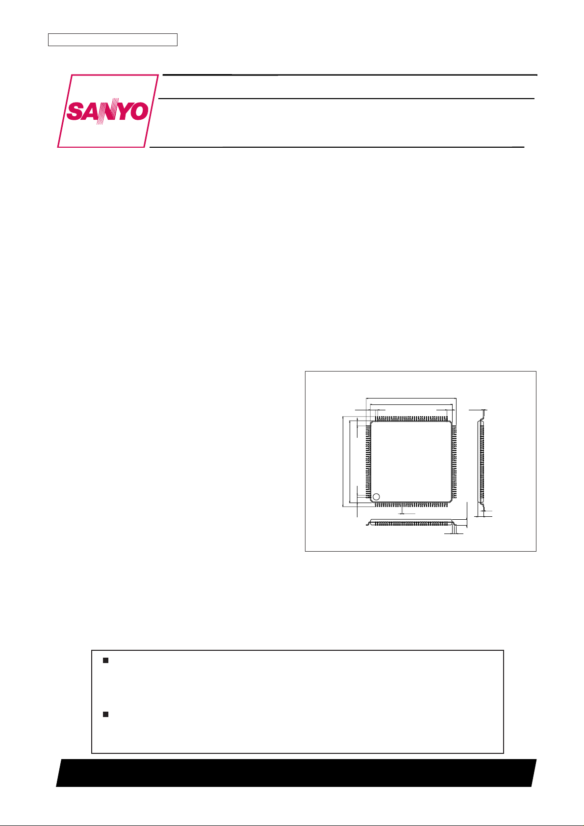
• Package: SQFP-144
Package Dimensions
unit: mm
3214-SQFP144
LC895199K
SANYO Electric Co.,Ltd. Semiconductor Company
TOKYO OFFICE Tokyo Bldg., 1-10, 1 Chome, Ueno, Taito-ku, TOKYO, 110-8534 JAPAN
32× CD-ROM Decoder with ATAPI (IDE) Interface
CMOS IC
0.20
1.25
1.25
22.0
20.0
0.5
22.0
20.0
0.5
1.25
1.25
0.145
0.1
1.4
1.6max
0.5
0.5
136
37
72
73
108
109
144
SANYO: SQFP144
[LC895199K]
Any and all SANYO products described or contained herein do not have specifications that can handle
applications that require extremely high levels of reliability, such as life-support systems, aircraft’s
control systems, or other applications whose failure can be reasonably expected to result in serious
physical and/or material damage. Consult with your SANYO representative nearest you before using
any SANYO products described or contained herein in such applications.
SANYO assumes no responsibility for equipment failures that result from using products at values that
exceed, even momentarily, rated values (such as maximum ratings, operating condition ranges, or other
parameters) listed in products specifications of any and all SANYO products described or contained
herein.
Page 2
No. 6238-2/12
LC895199K
Parameter Symbol Conditions Ratings Unit
Maximum supply voltage
V
DD
5 max Ta = 25°C –0.3 to +6.0 V
V
DD
3 max Ta = 25°C –0.3 to +4.6 V
Input/output voltage
V
I
15, VO5 Ta = 25°C –0.3 to VDD5 + 0.3 V
V
I
13, VO3 Ta = 25°C –0.3 to VDD3 + 0.3 V
Allowable power dissipation Pd max Ta ≤ 70°C 550 mW
Operating temperature Topr –30 to +70 °C
Storage temperature Tstg –55 to +125 °C
Soldering temperature (pin part only) 10 s 235 °C
Input/output power I
I
, I
O
* ±20 mA
Specifications
Absolute Maximum Ratings at VSS= 0 V
Note: * Per 1 input/output reference cell
Changes from the LC895199
Items changed from the LC895199-MK2
• Revision 4.
• The DVD-ROM and DVD-RAM interface functions
have been removed.
• The buffer circuits for the DRAM pins (RAS, CAS0,
CAS1, OE, WE, and A0 to A8) have been changed from
8 mA sink to 4 mA sink.
• The buffer circuits for the D/A converter output pins
(DSDATA, DLRCK, DBCK) have been changed from
8 mA sink to 4 mA sink.
• The amount of external DRAM supported has been
changed from 16M to 4M.
• The MCK3 output has been changed to a 1/1, 1/2, stop
output.
• Settings have been added for cases when the PLL circuit
is not used. (W register R46 bit 7 (set to 1) and C
register R1 (set to 40h))
Parameter Symbol Conditions
Ratings
Unit
min typ max
Supply voltage V
DD
3.0 3.3 3.6 V
Input voltage range V
IN
0V
DD
V
Internal Cell 3.3 V Supply Voltage
Allowable Operating Range at Ta = –30 to +70°C, VSS= 0 V
Parameter Symbol Conditions
Ratings
Unit
min typ max
Supply voltage V
DD
4.5 5.0 5.5 V
Input voltage range V
IN
0V
DD
V
IOCell 5.0 V Supply Voltage
Page 3
No. 6238-3/12
LC895199K
Parameter Symbol Conditions Applicable pins
*1
Ratings
Unit
min typ max
Input high-level voltage V
IH
TTL levels
(1)
2.2——V
Input low-level voltage V
IL
— — 0.8 V
Input high-level voltage V
IH
TTL levels
(10)
2.2——V
Input low-level voltage V
IL
with pull-down resistor — — 0.8 V
Input high-level voltage V
IH
TTL levels
(2), (3), (11)
2.4——V
Input low-level voltage V
IL
Schmitt — — 0.8 V
Output high-level voltage V
OHIOH1
= –4 mA
(4)
VDD– 2.1 — — V
Output low-level voltage V
OLIOL1
= 4 mA — — 0.4 V
Output high-level voltage V
OHIOH1
= –8 mA
(10), (12)
VDD– 2.1 — — V
Output low-level voltage V
OLIOL1
= 8 mA — — 0.4 V
Output high-level voltage V
OHIOH1
= –12 mA
(5)
VDD– 2.1 — — V
Output low-level voltage V
OLIOL1
= 12 mA — — 0.4 V
Output high-level voltage V
OHIOH1
= –12 mA
(5)
VDD– 2.1 — — V
Output low-level voltage V
OLIOL1
= 12 mA — — 0.4 V
Output high-level voltage V
OHIOH1
= –4 mA
(8), (11)
VDD– 2.1 — — V
Output low-level voltage V
OLIOL1
= 24 mA — — 0.4 V
Output low-level voltage V
OLIOL1
= 24 mA (9) — — 0.4 V
Output low-level voltage V
OLIOL1
= 8 mA (6), (7) — — 0.4 V
Input leakage current I
IL
VI= VSS, V
DD
(1), (2), (3), (11) –10 +10 µA
Output leakage current I
OZ
During high-impedance output (6), (8), (9), (11)
–10 +10 µA
Pull-up resistance R
UP
(10) 40 80 160 kΩ
Pull-up resistance R
UP
ZDMACK *
2
(7) 20 40 80 kΩ
DC Characteristics at Ta = –30 to +70°C, VSS= 0 V, VDD= 4.5 to 5.5 V
Notes:1. The applicable pin sets are as follows.
2. When ZDMACK is reset, internal pull-up resistor is OFF.
When Config-Reg-R46 (PULON)-bit 0 (ZDMACK) = 1, pull-up resistor becomes ON.
INPUT
(1) ATPINSEL, CSCTRL, SUA0 to SUA6, BCK, C2PO, LRCK, SDATA, SBS0, SCOR, WFCK, TEST0 to TEST1
(2) ZRESET, ZCS, ZRD, ZWR, CSEL
(3) DA0 to DA2, ZCS1FX, ZCS3FX, ZDIOR, ZDIOW, ZDMACK, ZHRST
OUTPUT
(4) RA0 to RA8, ZRAS0, ZCAS0 to ZCAS1, ZUWE, ZLWE, ZOE
(5) MCK, MCK3
(6) ZRSTCPU
(7) ZINT, ZINT1, ZSWAIT
(8) DMARQ, HINTRQ
(9) IORDY, ZIOCS16
INOUT
(10) D0 to D7, IO0 to IO15, HDB0 to HDB7
(11) DD0 to DD15, ZDASP, ZPDIAG
(12) EXCK
Note: Pins XTAL and XTALCK are not included in the DC characteristics.
Page 4
No. 6238-4/12
LC895199K
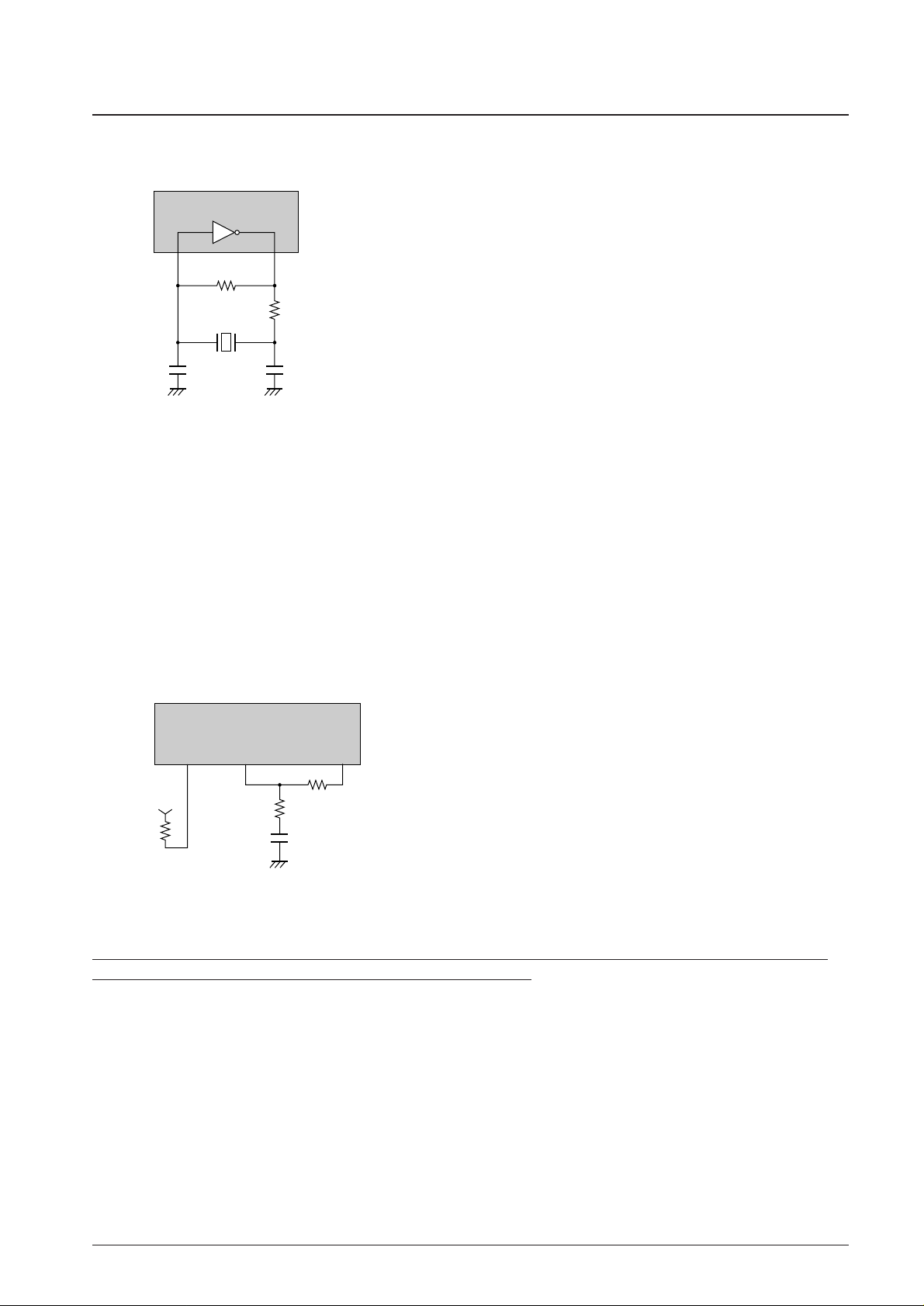
Recommended Oscillator Circuit
LC895199K
R1
R2
C2C1
XTALCK
PN52
XTAL
PN53
A12521
R1 = 1 MΩ
R2 = 47 Ω
C1 = 0
C2 = 47 pF
Ceramic oscillator frequency = 33.8688 MHz.
The 33.8688 MHz frequency in the recommended circuit is the third harmonic.
Since the exact values of these components will vary depending on characteristics of the printed circuit board used and
other factors, consult the manufacturer of the oscillator element when designing the oscillator circuit.
External Circuits for the On-Chip PLL Version (LC895199)
PN69 PN70 PN71
LC895199K
PLL
R5
Analog V
SS
R4
C3
R3
3.3V
A12522
R3 = 5.1 kΩ, R4 = 200 Ω, R5 = 10 kΩ, C3 = 0.1 µF
The analog VDDand VSSmust be made completely independent of the logic system power supply. In particular, they
must not be affected by fluctuations in the logic system power supply.
Page 5

No. 6238-5/12
LC895199K
Block Diagram
Sub-code I/F
10byte FIFO for Sub Q
Address generator
Address generator
DAC
CAV-Audio contorol
De-scramble &
Buffering
Address generator
Microcontroller
RAM access
Address generator
Address generator
ECC & EDC
Based HISIDE
IDE I/F
Address generator
Data output input I/F
Bus
Arbiter
&
DRAM
controller
External
Buffer
DRAM
Each Block
Bus control
signal
Each Block
Register
R0-R127
CD-DSP I/F
& SYNC
Detector
Reset
Controller
CD-DSP
HOST
Micro
controller
decoder
Clock generator
& PLL
*1
*2
*8
*10
*9
*6
*7
*11
*3
*5
*4
EXCK
ZRESET
ZINT0
ZINT1
ZSWAIT
ZRSTCPU
XTALCK
XTAL
MCK3
MCK
Each Block
Data bus[0:7]
Address bus[0:17]
RAM
Data bus[0:15]
LC895199K
**1
A12523
*1 WFCK, SBSO, SCOR
*2 BCK, SDATA, LRCK, C2PO
*3 DD0 to DD15, ZDASP, ZPDIAG
*4 ZCS1FX, ZCS3FX, DA0 to DA2, ZDIOR, ZDIOW, ZDMACK, CSEL
*5 DMARQ, HINTRQ, ZIOCS16, IORDY, ZHRST
*6 ZRD, ZWR, SUA0 to SUA6, ZCS, CSCTRL
*7 D0 to D7
*8 IO0 to IO15
*9 RA0 to RA8, ZRAS0, ZCAS0, ZCAS1, ZOE, ZUWE, ZLWE
*10 DBCK, DLRCK, DSDATA
*11 IOP0 to IOP7
**1 HISIDE(WD25C32) is made by WESTERN DIGITAL
Page 6

No. 6238-6/12
LC895199K
Pin Functions
LC895199K Pin Functions
(When pin 103 (ATPINSEL) is low)
Type
I INPUT B BIDIRECTION NC NOT CONNECT
O OUTPUT P POWER
Pin No. Pin name Type Pin functions
1V
SS0
P
2 ZRAS0 O Buffer DRAM RAS signal output
3 ZCAS0 O Buffer DRAM CAS signal output 0 (Normally held at 0 (low).)
4 ZCAS1 O Buffer DRAM CAS signal output 1
5V
SS0
P
6 ZOE O Buffer DRAM output enable
7 ZUWE O Buffer DRAM upper write enable
8 ZLWE O Buffer DRAM lower write enable
9V
SS0
P
10 RA0 O
11 RA1 O
12 RA2 O
13 RA3 O
Data buffer DRAM address signal outputs
14 RA4 O
15 RA5 O
16 RA6 O
17 RA7 O
18 V
DD0
P 5.0 V
19 V
SS0
P
20 RA8 O Data buffer DRAM address signal output
21 IO0 B
22 IO1 B
23 IO2 B Data buffer DRAM data input and output
24 IO3 B These pins have built-in pull-up resistors.
25 IO4 B
26 IO5 B
27 V
SS0
P
28 IO6 B
29 IO7 B
30 IO8 B
31 IO9 B Data buffer DRAM data input and output
32 IO10 B These pins have built-in pull-up resistors.
33 IO11 B
34 IO12 B
35 IO13 B
36 V
SS0
P
37 V
DD1
P 3.3 V
38 IO14 B Data buffer DRAM data input and output
39 IO15 B These pins have built-in pull-up resistors.
40 NC
41 V
SS0
P
42 IOP0 B
43 IOP1 B
44 IOP2 B
45 IOP3 B
General-purpose input and output ports
46 IOP4 B
47 IOP5 B
48 IOP6 B
49 IOP7 B
50 NC
51 TEST0 I Test pin. This pin must be connected to V
SS
in normal operation.
52 XTALCK I Crystal oscillator circuit input
Continued on next page.
Page 7

No. 6238-7/12
LC895199K
Continued from preceding page.
Pin No. Pin I/O Function
53 XTAL O Crystal oscillator circuit output
54 V
DD0
P 5.0 V
55 V
SS0
P
56 MCK O XTALCLK 1/1, 1/2, and stop output
57 TEST1 I Test pin. This pin must be connected to V
SS
in normal operation.
58 DSDATA O
59 DLRCK O D/A converter outputs
60 DBCK O
61 C2PO I
62 SDATA I
CD DSP interface
63 BCK I
64 LRCK I
65 EXCK O
66 WFCK I
Subcode input and output
67 SBSO I
68 SCOR I
69 PLL1
70 PLL2 PLL circuit connections
71 PLL3
72 V
SS0
P (This is an analog VSSpin in the LC895199 built-in PLL version.)
73 V
DD1
P 3.3 V (This is an analog VDDpin in the LC895199 built-in PLL version.)
74 ZRESET I IC reset
75 MCK3 O XTALCLK 1/1, 1/5, 2/5, 1/512, and stop output
76 CSCTRL I Microcontroller CS pin active low/active high selection
77 ZRD I Microcontroller data read signal input
78 ZWR I Microcontroller data write signal input
79 ZCS I Register chip select input from the microcontroller
80 SUA0 I
81 SUA1 I
82 SUA2 I
83 SUA3 I Microcontroller register selection signals
84 SUA4 I
85 SUA5 I
86 SUA6 I
87 D0 B
Microcontroller data signals
88 D1 B
These pins have built-in pull-up resistors.
89 D2 B
90 V
DD0
P 5.0 V
91 V
SS0
P
92 D3 B
93 D4 B
Microcontroller data signals
94 D5 B
These pins have built-in pull-up resistors.
95 D6 B
96 D7 B
97 ZINT0 O
Interrupt request signal output to the microcontroller
98 ZINT1 O
99 ZSWAIT O Wait signal output to the microcontroller
100 ZRSTCPU O CPU reset signal
101 CSEL I
ATAPI control signals
102 ZHRST I
103 ATPINSEL I ATAPI pin layout selection. (This pin must be connected to V
SS0
.)
104 ZDASP B
105 ZCS3FX I
106 ZCS1FX I
107 DA2 I
Continued on next page.
Page 8

No. 6238-8/12
LC895199K
Continued from preceding page.
Pin No. Pin I/O Function
108 V
SS1
P
109 V
DD1
P 3.3 V
110 DA0 I
111 ZPDIAG B
112 DA1 I
ATAPI control signals
113 ZIOCS16 O
114 HINTRQ O
115 ZDMACK I
116 V
SS1
P
117 IORDY O
118 ZDIOR I
ATAPI control signals
119 ZDIOW I
120 DMARQ O
121 V
SS1
P
122 DD15 B
123 DD0 B
ATAPI data bus
124 DD14 B
125 DD1 B
126 V
DD0
P 5.0 V
127 V
SS1
P
128 DD13 B
129 DD2 B
ATAPI data bus
130 DD12 B
131 DD3 B
132 V
SS1
P
133 DD11 B
134 DD4 B ATAPI data bus
135 DD10 B
136 V
SS1
P
137 V
DD0
P 5.0 V
138 DD5 B
139 DD9 B ATAPI data bus
140 DD6 B
141 V
SS1
P
142 DD8 B
ATAPI data bus
143 DD7 B
144 V
DD1
P 3.3 V
Unused (“NC”) pins must be left open.
Pins whose name begin with Z operate with inverted (negative) logic.
V
SS0
is the logic system ground and V
SS1
is the IDE interface driver ground.
Applications must supply 5.0 V for V
DD0
and 3.3 V for V
DD1
.
Page 9

No. 6238-9/12
LC895199K
Pin Functions
LC895199K Pin Functions
(When pin 103 (ATPINSEL) is high)
Type
I INPUT B BIDIRECTION NC NOT CONNECT
O OUTPUT P POWER
Pin No. Pin name Type Pin functions
1V
SS0
P
2 ZRAS0 O Buffer DRAM RAS signal output
3 ZCAS0 O Buffer DRAM CAS signal output 0 (Normally held fixed at 0 (low).)
4 ZCAS1 O Buffer DRAM CAS signal output 1
5V
SS0
P
6 ZOE O Buffer DRAM output enable
7 ZUWE O Buffer DRAM upper write enable
8 ZLWE O Buffer DRAM lower write enable
9V
SS0
P
10 RA0 O
11 RA1 O
12 RA2 O
13 RA3 O
Data buffer DRAM address signal outputs
14 RA4 O
15 RA5 O
16 RA6 O
17 RA7 O
18 V
DD0
P 5.0 V
19 V
SS0
P
20 RA8 O Data buffer DRAM address signal output
21 IO0 B
22 IO1 B
23 IO2 B Data buffer DRAM data input and output
24 IO3 B These pins have built-in pull-up resistors.
25 IO4 B
26 IO5 B
27 V
SS0
P
28 IO6 B
29 IO7 B
30 IO8 B
31 IO9 B Data buffer DRAM data input and output
32 IO10 B These pins have built-in pull-up resistors.
33 IO11 B
34 IO12 B
35 IO13 B
36 V
SS0
P
37 V
DD1
P 3.3 V
38 IO14 B Data buffer DRAM data input and output
39 IO15 B These pins have built-in pull-up resistors.
40 NC
41 V
SS0
P
42 IOP0 B
43 IOP1 B
44 IOP2 B
45 IOP3 B
General-purpose input and output ports
46 IOP4 B
47 IOP5 B
48 IOP6 B
49 IOP7 B
50 NC
51 TEST0 I Test pin. This pin must be connected to V
SS
in normal operation.
52 XTALCK I Crystal oscillator circuit input
Continued on next page.
Page 10

No. 6238-10/12
LC895199K
Continued from preceding page.
Pin No. Pin I/O Function
53 XTAL O Crystal oscillator circuit output
54 V
DD
P 5.0 V
55 V
SS0
P
56 MCK O XTALCLK 1/1, 1/2, and stop output
57 TEST1 I Test pin. This pin must be connected to V
SS
in normal operation.
58 DSDATA O
59 DLRCK O D/A converter outputs
60 DBCK O
61 C2PO I
62 SDATA I
CD DSP interface
63 BCK I
64 LRCK I
65 EXCK O
66 WFCK I
Subcode input and output
67 SBSO I
68 SCOR I
69 PLL1
70 PLL2 PLL circuit connections
71 PLL3
72 V
SS0
P (This is an analog VSSpin in the LC895199 built-in PLL version.)
73 V
DD1
P 3.3 V (This is an analog VDDpin in the LC895199 built-in PLL version.)
74 ZRESET I IC reset
75 MCK3 O XTALCLK 1/1, 1/5, 2/5, 1/512, and stop output
76 CSCTRL I Microcontroller CS pin active low/active high selection
77 ZRD I Microcontroller data read signal input
78 ZWR I Microcontroller data write signal input
79 ZCS I Register chip select input from the microcontroller
80 SUA0 I
81 SUA1 I
82 SUA2 I
83 SUA3 I Microcontroller register selection signals
84 SUA4 I
85 SUA5 I
86 SUA6 I
87 D0 B
Microcontroller data signals
88 D1 B
These pins have built-in pull-up resistors.
89 D2 B
90 V
DD0
P 5.0 V
91 V
SS0
P
92 D3 B
93 D4 B Microcontroller data signals
94 D5 B These pins have built-in pull-up resistors.
95 D6 B
96 D7 B
97 ZINT0 O
Interrupt request signal output to the microcontroller
98 ZINT1 O
99 ZSWAIT O Wait signal output to the microcontroller
100 ZRSTCPU O CPU reset signal
101 CSEL I ATAPI control signal
102 DD7 B ATAPI data bus
103 ATPINSEL I ATAPI pin layout selection. (This pin must be connected to V
DD0
.)
104 DD8 B
105 DD6 B
ATAPI data bus
106 DD9 B
107 DD5 B
Continued on next page.
Page 11

No. 6238-11/12
LC895199K
Continued from preceding page.
Pin No. Pin I/O Function
108 V
SS1
P
109 V
DD1
P 3.3 V
110 DD10 B
111 DD4 B
112 DD11 B
ATAPI data bus
113 DD3 B
114 DD12 B
115 DD2 B
116 V
SS1
P
117 DD13 B
118 DD1 B
ATAPI data bus
119 DD14 B
120 DD0 B
121 V
SS1
P
122 DD15 B ATAPI data bus
123 DMARQ O
124 ZDIOW I ATAPI control signal
125 ZDIOR I
126 V
DD0
P 5.0 V
127 V
SS1
P
128 IORDY O
129 ZDMACK I
ATAPI control signal
130 HINTRQ O
131 ZIOCS16 O
132 V
SS1
P
133 DA1 I
134 ZPDIAG B ATAPI control signal
135 DA0 I
136 V
SS1
P
137 V
DD0
P 5.0 V
138 DA2 I
139 ZCS1FX I ATAPI control signal
140 ZCS3FX I
141 V
SS1
P
142 ZDASP B
143 ZHRST I
144 V
DD1
P 3.3 V
Unused (“NC”) pins must be left open.
Pins whose name begin with Z operate with inverted (negative) logic.
V
SS0
is the logic system ground and V
SS1
is the IDE interface driver ground.
Applications must supply 5.0 V for V
DD0
and 3.3 V for V
DD1
.
Page 12

PS No. 6238-12/12
LC895199K
This catalog provides information as of February, 2000. Specifications and information herein are subject
to change without notice.
Specifications of any and all SANYO products described or contained herein stipulate the performance,
characteristics, and functions of the described products in the independent state, and are not guarantees
of the performance, characteristics, and functions of the described products as mounted in the customer’s
products or equipment. To verify symptoms and states that cannot be evaluated in an independent device,
the customer should always evaluate and test devices mounted in the customer’s products or equipment.
SANYO Electric Co., Ltd. strives to supply high-quality high-reliability products. However, any and all
semiconductor products fail with some probability. It is possible that these probabilistic failures could
give rise to accidents or events that could endanger human lives, that could give rise to smoke or fire,
or that could cause damage to other property. When designing equipment, adopt safety measures so
that these kinds of accidents or events cannot occur. Such measures include but are not limited to protective
circuits and error prevention circuits for safe design, redundant design, and structural design.
In the event that any or all SANYO products (including technical data, services) described or contained
herein are controlled under any of applicable local export control laws and regulations, such products must
not be exported without obtaining the export license from the authorities concerned in accordance with the
above law.
No part of this publication may be reproduced or transmitted in any form or by any means, electronic or
mechanical, including photocopying and recording, or any information storage or retrieval system,
or otherwise, without the prior written permission of SANYO Electric Co., Ltd.
Any and all information described or contained herein are subject to change without notice due to
product/technology improvement, etc. When designing equipment, refer to the “Delivery Specification”
for the SANYO product that you intend to use.
Information (including circuit diagrams and circuit parameters) herein is for example only; it is not
guaranteed for volume production. SANYO believes information herein is accurate and reliable, but
no guarantees are made or implied regarding its use or any infringements of intellectual property rights
or other rights of third parties.
 Loading...