

SANYO LC895195 Datasheet
Overview
The LC895195 is a CD-ROM decoder LSI that includes
both an on-chip IDE interface that was developed jointly
with Western Digital and an on-chip subcode ECC
function.
Features
• ATA-PI (IDE) interface
• Supports 16× playback (with IORDY) - Using ×16 70 ns
DRAMs
• 16.6 MB/s transfer rate: Using ×16 70 ns DRAMs
• 8.33 MB/s transfer rate: Using ×8 70 ns DRAMs
• Supports the use of from 1 M to 32 M of buffer RAM.
(DRAM)
• Allows the user to arbitrarily set the CD main channel,
C2 flag and subcode areas in buffer RAM.
• Batch transfer function (function for transferring the CD
main channel, C2 flag and subcode data in one
operation)
• Multi-transfer function (function for sending multiple
blocks in one operation)
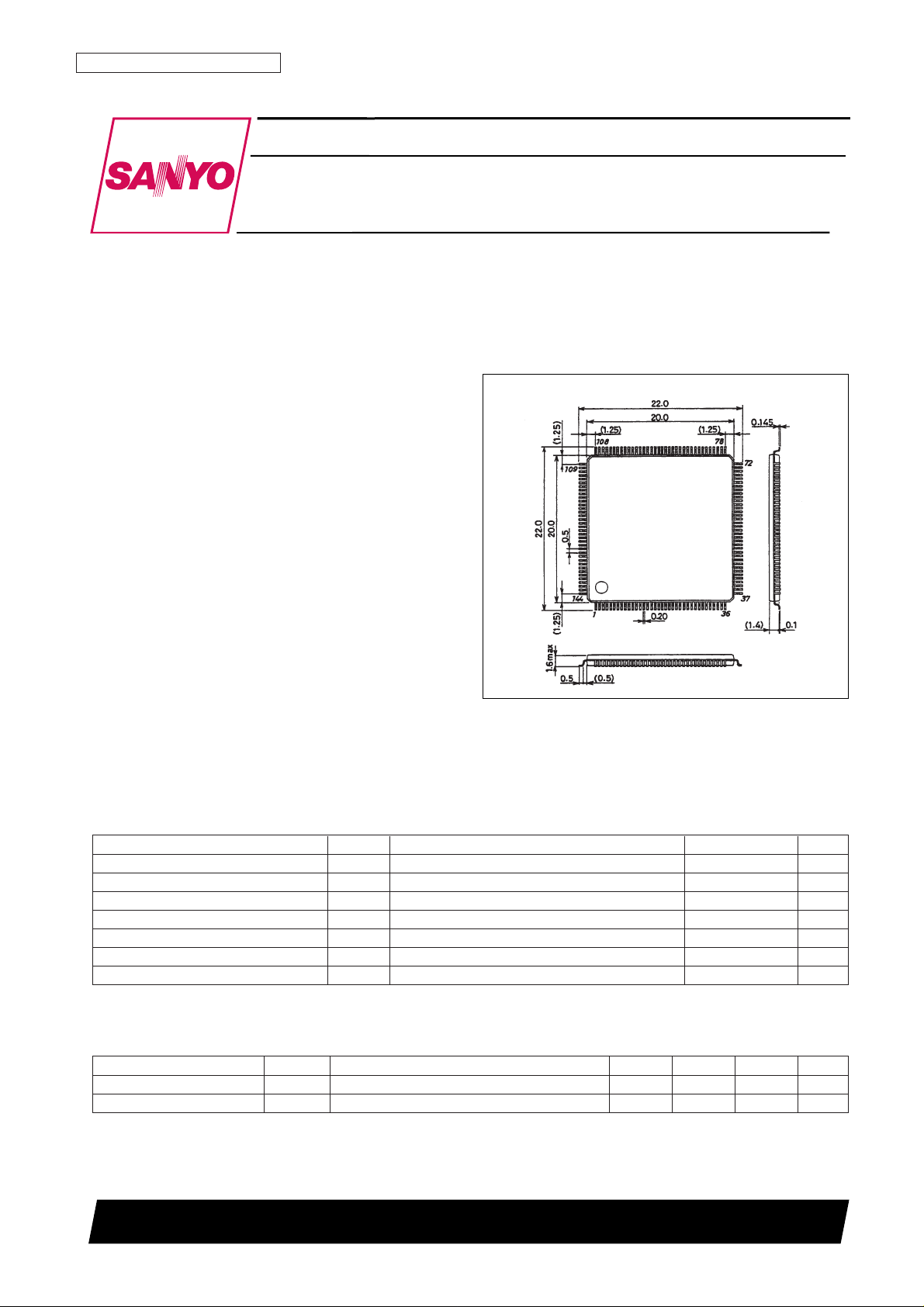
Package Dimensions
unit: mm
3214-SQFP144
CMOS LSI
Ordering number : EN* 5192B
N3097HA (OT)/22896HA (OT) No. 5192-1/8
Preliminary
SANYO: SQFP144
[LC895195]
SANYO Electric Co.,Ltd. Semiconductor Bussiness Headquarters
TOKYO OFFICE Tokyo Bldg., 1-10, 1 Chome, Ueno, Taito-ku, TOKYO, 110 JAPAN
ATA-PI (IDE) CD-ROM Decoder LSI
LC895195
Specifications
Absolute Maximum Ratings at VSS= 0 V
Note: * Per cell for basic I/O cells
Allowable Operating Ranges at Ta = –30 to +75°C, VSS= 0 V
Parameter Symbol Conditions Ratings Unit
Maximum supply voltage V
DD
max Ta = 25°C –0.3 to +7.0 V
I/O voltages V
I
, VOmax Ta = 25°C –0.3 to VDD+ 0.3 V
Allowable power dissipation Pd max Ta ≤ 70°C 550 mW
Operating temperature Topr –30 to +75 °C
Storage temperature Tstg –55 to +125 °C
Soldering heat resistances (pins only) 10 seconds 235 °C
I/O current I
I
, IOmax ±20* mA
Parameter Symbol Conditions min typ max Unit
Supply voltage V
DD
4.5 5.0 5.5 V
Input voltage range V
IN
0V
DD
V
No. 5192-2/8
LC895195
DC Characteristics at VSS= 0 V, VDD= 4.5 to 5.5 V, Ta = –30 to +75°C
Note: * The entries in the “Applicable Pins” column specify the following pin sets.
[Input]
1: CSCTRL, SUA0 to SUA6, TEST0 to TEST4
2: SBSO, SCOR, WFCK, ZCS, ZDIOR, ZDIOW, ZDMACK, ZHRST, ZRESET, ZRD, ZWR, BCK, C2PO, LRCK, SDATA, DA0 to DA2, ZCS1FX,
ZCS3FX
[Output]
3: MCK, MCK2
4: ZRSTCPU, ZRSTIC, ZINT1
5: ZINT, ZSWAIT
6: DMARQ, HINTRQ
7: RA0 to RA9, ZCAS0, ZCAS1, ZLWE, ZOE, ZRAS0, ZRAS1, ZUWE, EXCK
8: IORDY, ZIOCS16
[I/O]
9: D0 to D7, IO0 to IO15
10: DD0 to DD15, ZDASP, ZPDIAG
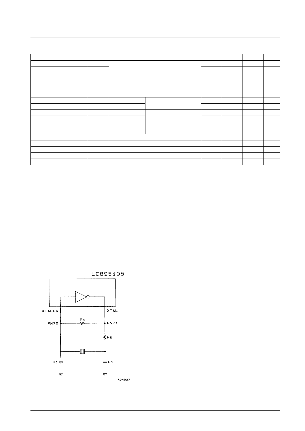
Note: XTAL, XTALCK
The above pins are not included in the DC characteristics.
Sample Recommended Oscillator Circuit
R1 = 120 kΩ
R2 = 47 kΩ
C1 = 30 pF
For a crystal oscillator frequency of 16.9344 MHz.
Alternatively:
R1 = 3.3 kΩ
R2 = None
C1 = 5 pF
For a crystal oscillator frequency of 33.8688 MHz.
For an oscillator frequency of 33.8688, the third harmonic is used. This means that
precise component values will be influenced by the printed circuit board. Consult
the manufacturer of the crystal to determine the circuit constants for this frequency.
Parameter Symbol Applicable Pins* (See below) min typ max Unit
Input high level voltage V
IH
1
TTL compatible: (1)
2.2 V
Input low level voltage V
IL
1 0.8 V
Input high level voltage V
IH
2
TTL compatible, with pull-up resistor: (9)
2.2 V
Input low level voltage V
IL
2 0.8 V
Input high level voltage V
IH
3
TTL compatible, Schmitt: (2), and (10)
2.2 V
Input low level voltage V
IL
3 0.8 V
Output high level voltage V
OH
1 IOH= –2 mA
(5), (7), and (9)
VDD– 2.1 V
Output low level voltage V
OL
1 IOL= 2 mA 0.4 V
Output high level voltage V
OH
2 IOH= –8 mA
(3)
VDD– 2.1 V
Output low level voltage V
OL
2 IOL= 8 mA 0.4 V
Output high level voltage V
OH
3 IOH= –4 mA
(6), and (10)
VDD– 2.1 V
Output low level voltage V
OL
3 IOL= 24 mA 0.4 V
Output high level voltage V
OL
5 IOL= 24 mA: (8) 0.4 V
Output high level voltage V
OL
4 IOL= 2 mA: (4) 0.4 V
Input leakage current I
IL
VI= VSS, VDD: (1), (2),and (10) –10 +10 µA
Output leakage current I
OZ
For high-impedance outputs: (6), and (10) –10 +10 µA
Pull-up resistance R
UP
(9) 40 80 160 kΩ

No. 5192-3/8
LC895195
Pin Functions
Type: I: Input pin, O: Output pin, B: Bidirectional pin, P: Power supply pin, NC: No connection pin
Note: 1. NC (no connection) pins must be left open.
2. Pin names (signal names) that begin with a Z have negative (inverted) logic.
3. V
SS0
is the logic system ground and V
SS1
is the IDE interface driver ground.
Pin No. Symbol Type Function
1 V
SS0
P
2 ZRAS0 O Buffer DRAM RAS signal output 0 (This pin is used normally.)
3 ZRAS1 O Buffer DRAM RAS signal output 1
4 V
SS0
P
5 ZCAS0 O Buffer DRAM CAS signal output 0 (This pin is used normally.)
6 ZCAS1 O Buffer DRAM CAS signal output 1
7 V
SS0
P
8 ZOE O Buffer RAM output enable
9 ZUWE O Buffer RAM upper write enable
10 ZLWE O Buffer RAM lower write enable
11 RA0 O
12 RA1 O
13 RA2 O
14 RA3 O RA0 to RA6 are the data buffer DRAM address signal output.
15 RA4 O
16 RA5 O
17 RA6 O
18 V
DD
P
19 V
SS0
P
20 RA7 O
21 RA8 O RA7 to RA9 are the data buffer DRAM address signal output.
22 RA9 O
23 V
SS0
P
24 TEST0 NC
25 NC
26 TEST1 NC
27 TEST2 NC
28 TEST3 NC
29 NC
30 IO0 B
31 IO1 B
Data buffer DRAM data I/O
32 IO2 B
These pins have built-in pull-up resistors.
33 IO3 B
34 IO4 B
35 IO5 B
36 V
SS0
P
37 V
DD
P
38 IO6 B
39 IO7 B
40 IO8 B
41 IO9 B Data buffer DRAM data I/O
42 IO10 B These pins have built-in pull-up resistors.
43 IO11 B
44 IO12 B
45 IO13 B
46 IO14 B
47 IO15 B
48 EXCK O SUB-CODE I/O
49 WFCK I
50 SBSO I
 Loading...