

SANYO LC89515K Datasheet
Ordering number : EN4272C
O2095HA (OT)/12395TH (OT)/ 61394TH No. 4272-1/6
Overview
The LC89515K is a version of the LC8951 in which
certain aspects of the internal registers have been
improved to make them even easier to use in CD-ROM
and CD-I products. The basic blocks are identical to those
in the LC8951 and these products are software and pin
compatible. Thus this product can replace the LC8951
without change. (However, this product is provided in a
slightly different package: a short lead type QIP-80E as
opposed to the QIP-80A.)
The LC89515K is an error correction and host interface
LSI for use in CD-ROM and CD-I products. This product
integrate in a single chip all CD-ROM specific functions,
including the error correction that was previously
implemented in software on a microprocessor and the CD
player and host computer interfaces that were previously
implemented in discrete components or gate arrays. The
use of the LSI can provide significant improvements in
CD-ROM and CD-I players, including increased transfer
rates, miniaturization, increased reliability, an improved
cost performance ratio, and a more efficient development
period.
Features
• Software and pin compatibility with the LC8951
(Changes were made to internal registers, the SRAM
interface, and other aspects.)
• Support for CD-ROM (mode 1) and CD-I (mode 2,
forms 1 and 2)
• All CD-ROM/CD-I special functions implemented on a
single chip
• Hardware error detection and correction for high speed,
without relying on software
• Real-time error correction: Error correction and
detection are possible without interrupting the host
interface bus.
• Fast transfers: up to 2.3 MB/s (18.4 Mb/s)
• Support for low-speed hosts (multiple block buffering)
• Built-in host interface command FIFO (for easy SCSI
support)
• Built-in 12-byte status FIFO
• CMOS circuits, single 5 V power supply
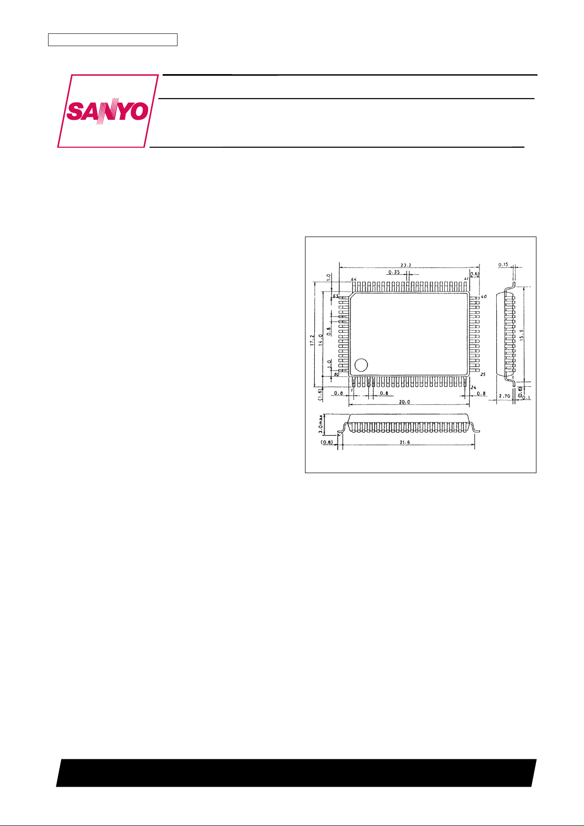
Package Dimensions
unit: mm
3174-QFP80E
SANYO: QIP80E
[LC89515K]
LC89515K
SANYO Electric Co.,Ltd. Semiconductor Bussiness Headquarters
TOKYO OFFICE Tokyo Bldg., 1-10, 1 Chome, Ueno, Taito-ku, TOKYO, 110-8534 JAPAN
CD-ROM/CD-I Error Correction/
Host Interface LSI
CMOS LSI
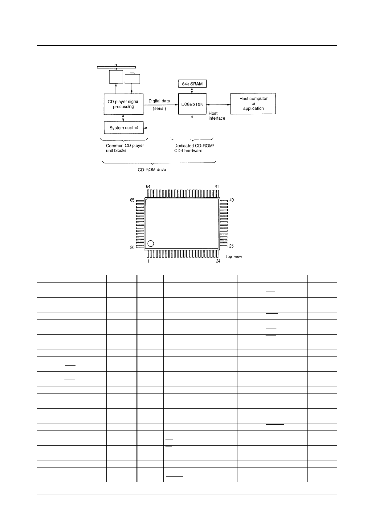
System Block Diagram
Pin Assignment
Type: I: Input pin, O: Output pin, B: Bidirectional pin, P: Power supply pin, NC: No connection
Note: Do not leave any of the V
DD
or VSSpins open. All of the VDDand VSSpins must be connected to ground or the power supply, respectively.
No. 4272-2/6
LC89515K
Pin No. Pin Type Pin No. Pin Type Pin No. Pin Type
1 V
SS
P 28 TEST2 I 55 HWR I
2 RA6 O 29 CSEL I 56 HRD I
3 RA7 O 30 LMSEL I 57 CMD I
4 RA8 O 31 V
DD
P 58 WAIT O
5 RA9 O 32 LRCK I 59 DTEN O
6 RA10 O 33 SDATA I 60 STEN O
7 RA11 O 34 BCK I 61 EOP O
8 RA12 O 35 C4LR I 62 RCS O
9 RA13 O 36 C2PO I 63 HDE O
10 RA14 O 37 MCK O 64 V
SS
P
11 RA15 O 38 D0 B 65 HD7 B
12 RWE O 39 D1 B 66 HD6 B
13 V
SS
P 40 D2 B 67 HD5 B
14 ROE O 41 V
SS
P 68 HD4 B
15 ERA B 42 D3 B 69 HD3 B
16 IO8 B 43 D4 B 70 HD2 B
17 IO7 B 44 D5 B 71 HD1 B
18 IO6 B 45 D6 B 72 HD0 B
19 IO5 B 46 D7 B 73 V
DD
P
20 IO4 B 47 RS I 74 SELDRQ I
21 IO3 B 48 RD I 75 RA0 O
22 IO2 B 49 WR I 76 RA1 O
23 IO1 B 40 CS I 77 RA2 O
24 V
SS
P 51 INT O 78 RA3 O
25 XTALCK I 52 V
SS
P 79 RA4 O
26 XTAL O 53 RESET I 80 RA5 O
27 TEST1 I 54 ENABLE I
 Loading...