

SANYO LC895124 Datasheet

Ordering number : EN*5240
22896HA (OT) No. 5240-1/8
Overview
The LC895124 is the next-generation version of the
LC89512 and is a CD-ROM decoder that includes a SCSI
interface that supports the high-speed transfers (10 MB/s)
of the FAST SCSI standard.
Functions
CD-ROM ECC function, subcode read function, SCSI
interface
Features
• On-chip SCSI interface (with built-in SCAM selection
register)
• Supports 8× playback - Using ×16 80-ns DRAMs
• Supports 4× playback - Using ×16 80-ns DRAMs or ×8
70-ns DRAMs
• Transfer rates: 10 MB/s (synchronous), 5 MB/s
(asynchronous) using ×16 80-ns DRAMs
*1
• Transfer rates: 8.467 MB/s (synchronous), 4.2336 MB/s
(asynchronous) using ×8 70-ns DRAMs
*2
• PSRAM can be used, providing 5 MB/s transfers in
synchronous mode and 5 MB/s transfers in
asynchronous mode .
• Supports the connection of up to 32 Mb of buffer RAM
(using DRAM) (Up to 2 Mb when PSRAM is used)
• The user can freely set the CD main channel, C2 flag,
and other areas in buffer RAM.
• Batch transfer function (transfers the CD main channel
and C2 flag data in a single operation)
• Multi-block transfer function (automatically transfers
multiple blocks in a single operation)
• High-speed transfer mode supports a 10-MB/s
(synchronous) transfer rate using ×8 80-ns DRAMs
• Subcode ECC function
Note: 1. For speeds up to 8× speed, use a SCSI master
clock frequency of 20 MHz.
Note: 2. For speeds up to 4× speed, use a SCSI master
clock frequency of 16.9344 MHz.
Package Dimensions
unit: mm
3214-SQFP144
Preliminary
SANYO: SQFP144
[LC895124]
LC895124
SANYO Electric Co.,Ltd. Semiconductor Bussiness Headquarters
TOKYO OFFICE Tokyo Bldg., 1-10, 1 Chome, Ueno, Taito-ku, TOKYO, 110-0005 JAPAN
CD-ROM Driver with On-Chip SCSI Interface and
Subcode Functions
CMOS LSI
Specifications
Absolute Maximum Ratings at VSS= 0 V
Parameter Symbol Conditions Ratings Unit
Maximum supply voltage V
DD
max Ta = 25°C –0.3 to +7.0 V
I/O voltages V
I
, V
O
Ta = 25°C –0.3 to VDD+ 0.3 V
Allowable power dissipation Pd max Ta ≤ 70°C 450 mW
Operating temperature Topr –30 to +70 °C
Storage temperature Tstg –55 to +125 °C
Soldering heat resistances (pins only) 10 seconds 260 °C

Allowable Operating Ranges at Ta = –30 to +70°C, VSS= 0 V
DC Characteristics at VSS= 0 V, VDD= 4.5 to 5.5 V, Ta = –30 to +70°C
Note: The subcode-related pins in group (1) are not provided by the LC895124.
SCSI Pin Input Characteristics
Sample Recommended Oscillator Circuit
R1 = 120 kΩ
R2 = 47 Ω
C1 = 30 pF
Crystal oscillator frequencies: XTALCK0 = 16.9344 MHz and XTALCK1 = 20 MHz
or:
R1 = 3.3 kΩ
R2 = None
C1 = 5 pF
Crystal oscillator frequency: XTALCK0 = 33.8688 MHz
If third harmonic overtones appear when using a 33.8688 MHz frequency with the
recommended circuit example, consult with the manufacturer of the crystal
element, since detailed values of the circuit constants will be influenced by the
printed circuit board.
No. 5240-2/8
LC895124
Parameter Symbol Applicable Pins min typ max Unit
Input high level voltage V
IH
1
All input pins other than (1), (3), and XTALCK
2.2 V
Input low level voltage V
IL
1 0.8 V
Input high level voltage V
IH
2
RESET, IO0 to IO15, D0 to D7, RD, CS, WR, WFCK,
2.5 V
Input low level voltage V
IL
2
SBSO, SCOR (1)
0.6 V
Input high level voltage V
IH
3
Input pins (3), ACK, and ATN
2.0 V
Input low level voltage V
IL
3 0.8 V
Output high level voltage V
OH
1
I
OH
1 = –2 mA: All output pins except (2), (3),
2.4 V
and XTALCK, IO0 to IO15, and D0 to D7
Output low level voltage V
OL
1
I
OL
1 = 2 mA: All output pins except (2), (3),
0.4 V
and XTALCK, IO0 to IO15, and D0 to D7
Output low level voltage V
OL
2
I
OL
2 = 2 mA: INT1, INT0, and ZSWAIT
0.4 V
(open-drain outputs with pull-up resistors) (2)
Output low level voltage V
OL
3
I
OL
3 = 48 mA: DB0, to DB7, DBP, BSY, I/O, MSG,
0.4 V
SEL, RST, REQ, C/D (3)
Input leakage current I
L
VI= VSS, VDD: All input pins –25 +25 µA
Pull-up resistance R
UP
IO0 to IO15, D0 to D7, INT0, INT1, ZSWAIT 40 80 160 kΩ
Parameter Symbol Conditions min typ max Unit
Supply voltage V
DD
4.5 5.0 5.5 V
Input voltage range V
IN
0 V
DD
V
Parameter Symbol Conditions min typ max Unit
Input threshold voltage
V
t + t1
VDD= 4.5 to 5.5 V
1.60 2.00 V
V
t – t1
0.80 1.11 V
Hysteresis width ∆V
tt1
VDD= 5.0 V 0.41 0.49 V
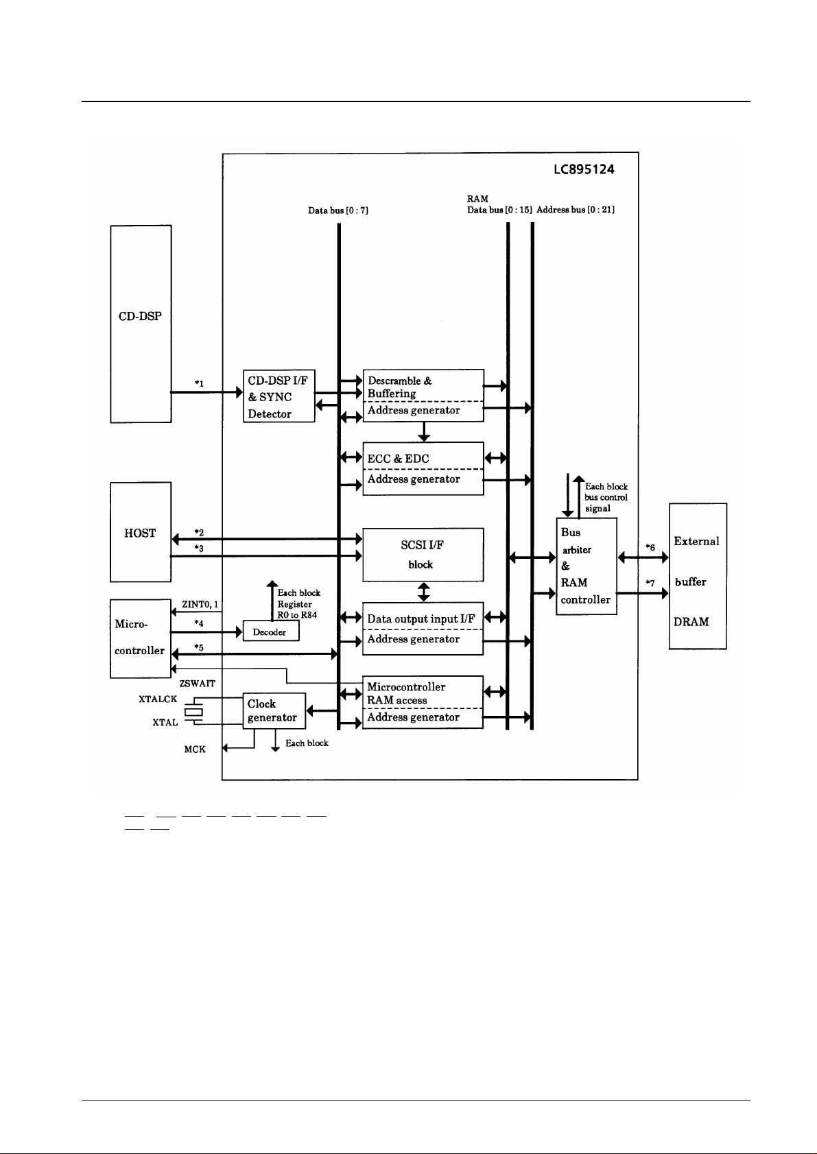
Block Diagram
Note: 1 BCK, SDATA, LRCK, C2PO
2. DB0 to DB7, DBP, BSY, MSG, SEL, RST, REQ, I/O, C/D
3. ACK, ATN
4. ZRD, ZWR, SUA0 to SUA6, ZCS, CSCTRL
5. D0 to D7
6. IO0 to IO15
7. RA0 to RA16, ZRAS0, ZRAS1, ZCAS0, ZCAS1, ZOE, ZUWE, ZLWE
Note: IO8 to IO15 and RA9 to RA16 are the same pins.
Subcode pins are connected to CD-DSP or to V
SS
.
No. 5240-3/8
LC895124
 Loading...