

SANYO LC89210 Datasheet
Overview
The LC89210 is a highly integrated modem engine that
can be used in products that support transmission rates up
to the 14,400 bps rate used in contemporary group III fax
equipment. The LC89210 is compatible with V.21, V.23
and Bell 103 full-duplex modems.
Features
• Supports the ITU-T V.17, V.29, and V.27ter fax
standards
• ITU-T V.23, V.21, and Bell 103
• V.17, V.29 (T104), and V.27ter short training
• V.33 half duplex
• 1800-Hz or 1700-Hz carrier
• The LC89210 is a complete data pump on a single chip.
• 5 V single-voltage power supply
— Operating power dissipation: 375 mW (typical)
— Low power mode: 5 mW (typical)
• Expanded operating modes
— Full implementation of V.17, V.33, V.29, and
V.27ter handshaking
— Autodial and autoanswer functions
— Programmable tone detection and FSK V.21 flag
pattern detection during high-speed reception
— Programmable call progresss and call waiting tone
detection, including DTMF
— Support for programmable CLASSTMdetection
— Wide dynamic range (better than 48 dB)
— A-law voice PCM mode
• Multiple interfaces
— Parallel 64 ×8-bit dual-port RAM
— Synchronous/HDLC parallel data processing
— Support for HDLC framing
— V.24 interface
— Can monitor all operating states in real time.
— Includes all diagnostic functions.
— Dual 8-bit D/A converter for eye pattern display
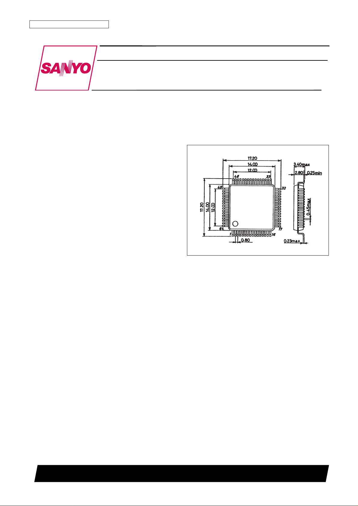
Package Dimensions
unit: mm
3213-PQFP64
CMOS LSI
52696HA (OT) No. 5382-1/10
Preliminaly
SANYO: PQFP64
[LC89210]
SANYO Electric Co.,Ltd. Semiconductor Bussiness Headquarters
TOKYO OFFICE Tokyo Bldg., 1-10, 1 Chome, Ueno, Taito-ku, TOKYO, 110 JAPAN
High-speed fax modem data pump
LC89210
Ordering number : EN*5382
No. 5382-2/10
LC89210
Specifications
Electrical Specifications at Ta = 25°C, VDD= 5 V (unless otherwise specified)
Absolute Maximum Ratings with respect to ground
Electrical Characteristics at Ta = 0 to +70°C, VDD= 5.0 V ± 5%, GND = 0 V (unless otherwise specified)
Parameter Symbol Conditions Ratings Unit
DC supply voltage V
DD
–0.3 to +7.0 V
Digital or analog input voltage V
I
, V
IN
–0.3 to (VDD+ 0.3) V
Digital or analog input current I
I
, I
IN
±1 mA
Digital output current I
O
±20 mA
Analog output current I
OUT
±10 mA
Allowable power dissipation Pd max 1000 mW
Operating temperature Topr 0 to +70 °C
Storage temperature (plastic) Tstg –40 to +125 °C
Parameter Symbol Conditions min typ max Unit
[Power Supply and Common-Mode Voltages]
Supply voltage V
DD
4.75 5 5.25 V
Current drain I
DD
75 100 mA
Current drain in lower power mode I
DD-ip
1 mA
Common-mode voltage V
CM
VDD/2 – 5% VDD/2 VDD/2 + 5% V
[Crystal Oscillator Interface] XTAL and EXTAL
Input low-level voltage V
IL
1.5 V
Input high-level voltage V
IH
3.5 V
Input low-level current I
L
GND < VI< VILmax –15 µA
Input high-level current I
H
VIHmin < VI< V
DD
15 µA
[Digital Interface] All digital pins except the XTAL pin
Input low-level voltage V
IL
–0.3 +0.8 V
Input high-level voltage V
IH
2.2 V
Input current I
I
VI= VDDor VI= GND –10 0 +10 µA
Output high-level voltage V
OHIlord
= 2 mA 2.4 V
Output low-level voltage V
OL
I
lord
= 2 mA 0.4 V
3-state input leakage current I
OZ
GND < VO< V
DD
–50 0 +50 µA
Input capacitance C
IN
5 pF
[Analog Interface]
Differential reference voltage input V
REF
V
REFP
– V
REFN
2.40 2.50 2.60 V
Input common-mode offset V
CMOin
V = (RXA1 + RXA2)/2 – V
CM
–300 +300 mV
Differential input voltage V
DIFin
RXA1 – RXA2 2 × V
REF
Vp-p
Output common-mode
V
CMOout
(TXA1 + TXA2)/2 – V
CM
–200 +200 mV
voltage offset
Differential output voltage V
DIFout
TXA1 – TXA2 2 × V
REF
Vp-p
Differential output DC offset V
OFFout
(TXA1 – TXA2) –100 +100 mV
Input resistance Rin RXA
X
100 kΩ
Output resistance Rout TXA
X
20 Ω
Load resistance R
L
TXA
X
10 kΩ
Load capacitance C
L
TXA
X
50 pF
No. 5382-3/10
LC89210
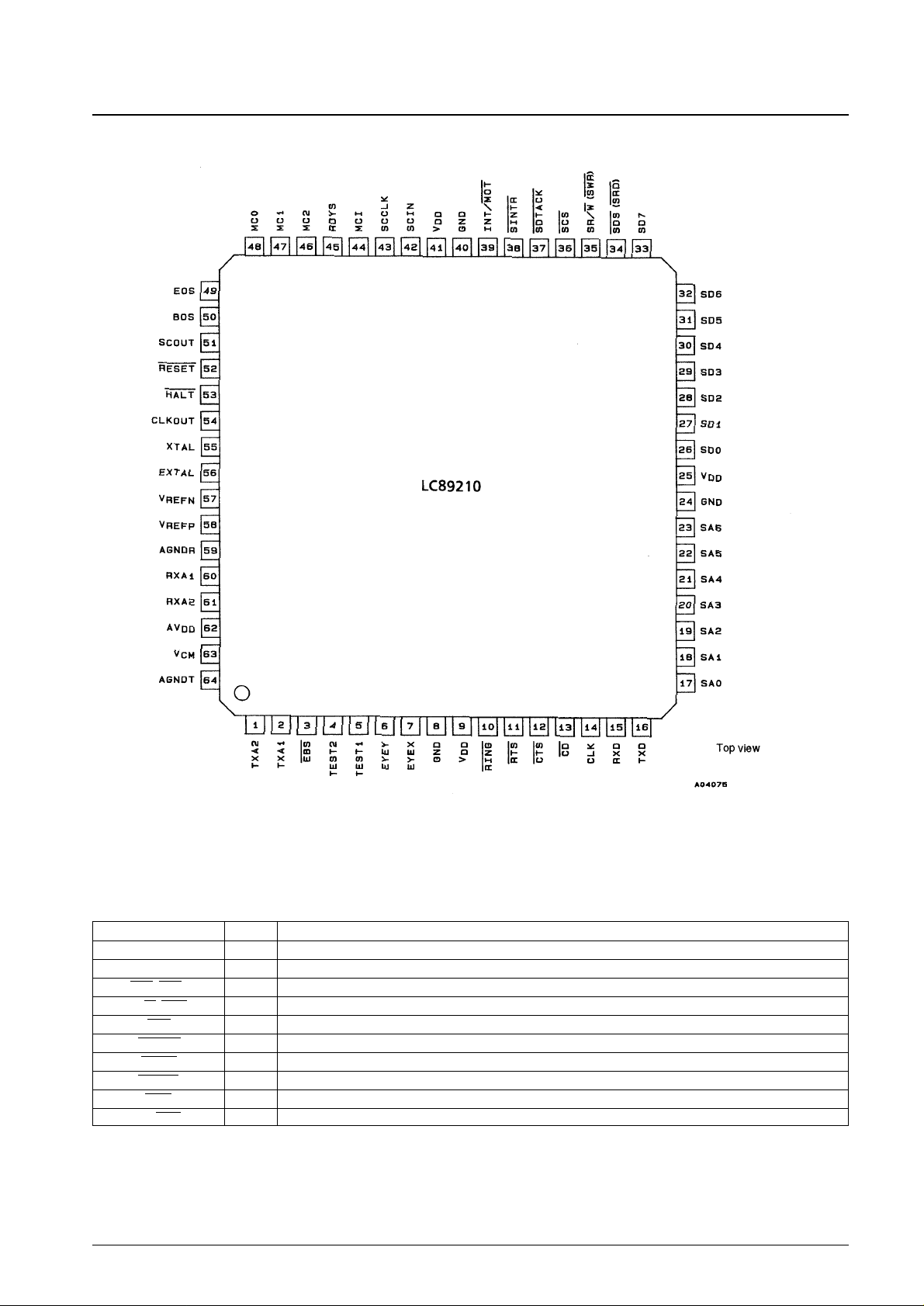
Pin Assignment
Host Interface
The LC89210 is interfaced to the control processor through a 64-byte dual-port RAM that is shared by the LC89210 and
the host.
Note: * Open-drain output
Pin Type Function
SD0 to SD7 I/O System data bus
SA0 to SA6 I System address bus
SDS (SDR) I System data strobe
SR/W (SWR) I System read/write
SCS I System chip select
SDTACK OD* System bus data acknowledge
SINTR OD* System interrupt request
RESET I Reset. This is an active-low signal.
RING I Ring detect signal
INT/MOT I Intel/Motorola interface
 Loading...