

SANYO LC89170M Datasheet
Overview
The LC89170M is an IC that decodes the text data, such
as song names, stored in subcode channels R to W of a
compact disk’s read-in area.
Features
• Accepts the channel R to W subcode data through a
subcode interface.
• Can continuously output the channel R to W data for
each 1PACK24 symbol.
• Performs error detection (cyclic redundancy code) and
outputs both the data and the result of that check.
• Provides synchronization protection for the subcode
interface.
• Supports low-voltage operation (3.3 V)
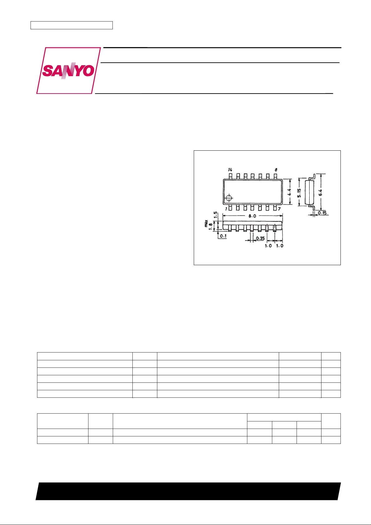
• Provided in the miniature MFP-14S package.
Package Dimensions
unit: mm
3111-MFP14S
CMOS LSI
Ordering number : EN*5536A
93096HA (OT) No. 5536-1/8
Preliminary
SANYO: MFP14S
[LC89170M]
SANYO Electric Co.,Ltd. Semiconductor Bussiness Headquarters
TOKYO OFFICE Tokyo Bldg., 1-10, 1 Chome, Ueno, Taito-ku, TOKYO, 110 JAPAN
CD Player Text Data IC
LC89170M
Specifications
Absolute Maximum Ratings at Ta = 25 °C, VSS= 0 V
Parameter Symbol Conditions Ratings Unit
Maximum supply voltage V
DD
max –0.3 to +7.0 V
I/O voltages V
IVO
–0.3 to VDD+ 0.3 V
Input current I
I
±10 mA
Operating temperature Topr –30 to +70 °C
Storage temperature Tstg –55 to +125 °C
Recommended Operating Conditions at Ta = 25 °C, VSS= 0 V
Parameter Symbol Conditions
Ratings
Unit
min typ max
Supply voltage V
DD
3.0 5.0 5.5 V
Operating temperature Topr –30 +70 V

Block Diagram
Pin Assignment
Pin Functions
No. 5536-2/8
LC89170M
Pin no. Symbol I/O Function
1 EXCK I/O Subcode interface shift clock input and output
2 SBSO I Subcode interface data input
3 SCOR I Subcode interface block synchronization input
4 WFCK I Subcode interface frame synchronization input
5 MCK I Clock input (16.9344 MHz)
6 XMODE I System reset and low power mode
7 GND Ground
8 TEST I Test pin (Must be connected to ground in normal operation.)
9 SW1 I EXCK I/O setting (L: clock output, H: clock input)
10 SW2 I EXCK clock output pulse width selection (L: double speed support, H: normal speed)
11 SCLK I Command interface shift clock input
12 SRDT O Command interface data output
13 DQSY O Command interface readout enable output
14 V
DD
Power supply

No. 5536-3/8
LC89170M
DC Characteristics
DC Characteristics (1) at Ta = –30 to +70°C, VDD= 4.5 to 5.5 V, VSS= 0 V
Note: 1. The MCK, TEST, SW1, and SW2 pins
2. The EXCK, SBSO, SCOR, WFCK, XMODE, and SCLK pins
3. The EXCK, SRDT, and DQSY pins
Parameter Symbol Conditions
Ratings
Unit
min typ max
Input high-level voltage V
IH
CMOS compatible; 1* 0.7 V
DD
V
CMOS compatible Schmitt; 2* 0.8 V
DD
V
Input low-level voltage V
IL
CMOS compatible; 1* 0.3 V
DD
V
CMOS compatible Schmitt; 2* 0.2 V
DD
V
Output high-level voltage V
OHIOH
= –2 mA; 3* VDD–2.1 V
Output low-level voltage V
OLIOH
= 2 mA; 3* 0.4 V
Current drain I
DD
VDD= 5 V, Ta = 25°C, MCK = 16.93 MHz 0.8 1.6 mA
V
DD
= 5 V, XMODE = [L] 60 120 µA
AC Characteristics
• The MCK pin
AC Characteristics (1) at Ta = –30 to +70°C, VDD= 3.0 to 5.5 V, VSS= 0 V
Parameter Symbol Conditions
Ratings
Unit
min typ max
High-level pulse width t
WH
25 56 ns
Low-level pulse width t
WL
25 56 ns
Pulse period t
C
58 100 ns
Rise and fall times t
R
, t
F
12 ns
DC Characteristics (2) at Ta = –30 to +70°C, VDD= 3.0 to 3.6 V, VSS= 0 V
Note: 1. The MCK, TEST, SW1, and SW2 pins
2. The EXCK, SBSO, SCOR, WFCK, XMODE, and SCLK pins
3. The EXCK, SRDT, and DQSY pins
Parameter Symbol Conditions
Ratings
Unit
min typ max
Input high-level voltage V
IH
CMOS compatible; 1* 0.7 V
DD
V
CMOS compatible Schmitt; 2* 0.75 V
DD
V
Input low-level voltage V
IL
CMOS compatible; 1* 0.2 V
DD
V
CMOS compatible Schmitt; 2* 0.15 V
DD
V
Output high-level voltage V
OHIOH
= –1 mA; 3* VDD–0.8 V
Output low-level voltage V
OLIOH
= 1 mA; 3* 0.4 V
Current drain I
DD
VDD= 3.3 V, Ta = 25°C, MCK = 16.93 MHz 0.5 1.0 mA
V
DD
= 3.3 V, XMODE = [L] 25 50 µA
 Loading...