

SANYO LC8905V Datasheet

Ordering number : EN*5237
D3095HA (OT) No. 5237-1/16
Overview
The LC8905V is for use in IEC 958 and EIAJ CP-1201
format data transmission between digital audio equipment.
This LSI is used on the receiving side, and handles
synchronization with the input signal and demodulation of
that signal to a normal format signal.
Features
• On-chip PLL circuit synchronizes with the transmitted
IEC 958 and EIAJ CP-1201 format signal.
• Provides 128fs, bit, and L/R clock outputs.
• System clock can be selected to be either 384fs or 512fs.
• Microprocessor interface code settings for different
output types
— Input pin, emphasis output, input bi-phase data
output, and validity flag output settings
— Audio data output format setting
— Channel status output (32-bit output for consumer
products)
— Subcode Q output with CRC flags (80 bits)
• Start ID and shortening ID detection for DAT (Digital
Audio Tape recorder) that use subcodes
• CMOS, single-voltage power supply
• Miniature package: SSOP-24
Package Dimensions
unit: mm
3175A-SSOP24
Preliminary
SANYO: SSOP24
[LC8905V]
LC8905V
SANYO Electric Co.,Ltd. Semiconductor Bussiness Headquarters
TOKYO OFFICE Tokyo Bldg., 1-10, 1 Chome, Ueno, Taito-ku, TOKYO, 110-8534 JAPAN
Digital Audio Interface Receiver
CMOS LSI

Pin Assignment
Pin Functions
No. 5237-2/16
LC8905V
Pin No. Symbol I/O Description
1 DIN1 I Data input with built-in amplifier (for coaxial or optical module input)
2 DIN2 I Data input (for optical module input)
3 E/DOUT O Emphasis, input bi-phase, and validity flag output
4 V
DD
Power supply
5 R I VCO gain control input
6 VIN I VCO free-running setting input
7 VCO O PLL low-pass filter setting
8 GND Ground
9 CKSEL I System clock selection input (384fs or 512fs)
10 XMODE I Reset input
11 AVOCK I PLL error lock avoidance clock input
12 TST1 I Test input (Must be connected to ground in normal operation)
13 TST2 I Test input (Must be connected to ground in normal operation)
14 SCLK/CL I Microprocessor interface clock input
15 XLAT/CE I Microprocessor interface latch/chip enable input
16 SWDT/DI I Microprocessor interface write data input
17 SRDT/DO O Microprocessor interface read data output
18 DQSY/LD O Microprocessor interface subcode Q and ID synchronization output
19 CKOUT O VCO clock output (free running, 384fs, or 512fs)
20 FS128 O 128fs clock output
21 BCK O Bit clock output
22 LRCK O L/R clock output (left channel = high, right channel = low)
23 DATAOUT O Audio data output
24 ERROR O PLL lock error mute output
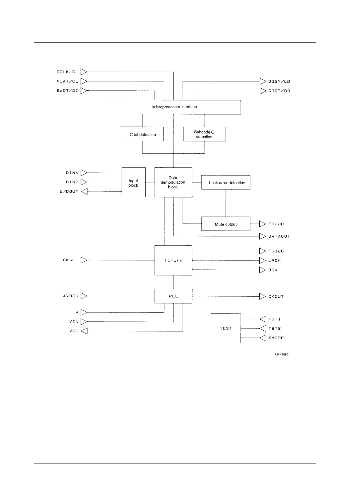
Block Diagram
No. 5237-3/16
LC8905V
Specifications
Absolute Maximum Ratings at Ta = 25°C
Allowable Operating Ranges
Electrical Characteristics
DC Characteristics at Ta = –30 to +75°C, VDD= 4.5 to 5.5 V, VSS= 0 V
AC Characteristics at Ta = –30 to +75°C, VDD= 4.5 to 5.5 V
No. 5237-4/16
LC8905V
Parameter Symbol Conditions Ratings Unit
Maximum supply voltage V
DD
max –0.3 to +7.0 V
Maximum I/O voltages V
IVO
max –0.3 to VDD+ 0.3 V
Operating temperature Topr –30 to +75 °C
Storage temperature Tstg –55 to +125 °C
Parameter Symbol Conditions min typ max Unit
Supply voltage V
DD
4.5 5.0 5.5 V
Parameter Symbol Conditions min typ max Unit
Input high-level voltage V
IH
1 Applies to the DIN2 pin. TTL levels 2.2 VDD+ 0.3 V
Input low-level voltage V
IL
1 Applies to the DIN2 pin. TTL levels –0.3 +0.8 V
Input high-level voltage V
IH
2
Applies to the CKSEL, AVOCK, TST1, and TST2 pins.
0.7 V
DD
VDD+ 0.3 V
CMOS levels
Input low-level voltage VIL2
Applies to the CKSEL, AVOCK, TST1, and TST2 pins.
–0.3 0.3 V
DD
V
CMOS levels
Input high-level voltage VIH3
Applies to the XMODE, SCLK/CL, XLAT/CE,
0.8 V
DD
VDD+ 0.3 V
SWDT/DI pins. CMOS Schmitt inputs
Input low-level voltage VIL3
Applies to the XMODE, SCLK/CL, XLAT/CE,
–0.3 0.2 V
DD
V
SWDT/DI pins. CMOS Schmitt inputs
Input high-level voltage V
OHIOH
= –1 µA VDD– 0.05 V
Input low-level voltage V
OL
IOL= 1 µA VDD+ 0.05 V
Current drain I
DD
VDD= 5.0 V, Ta = 25°C, input data fs = 48 kHz 10 15 mA
Input amplitude Vpp Measured before the DIN1 pin input capacitor. 0.4 V
DD
+ 0.3 V
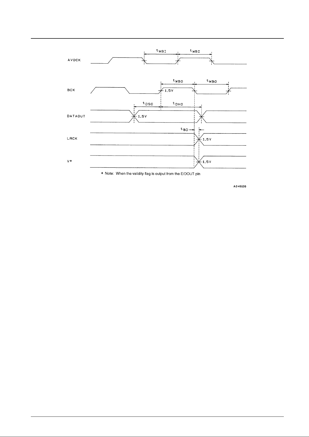
Parameter Symbol Conditions min typ max Unit
Input pulse width t
WBI
10 µs
Output pulse width t
WBO
fs = 48 kHz 160 ns
Output data setup time t
DSO
80 ns
Output data hold time t
DHO
80 ns
Output delay t
BD
–10 0 +10 ns
No. 5237-5/16
LC8905V
 Loading...