CMOS LSI
Ordering number : EN*5543
N3097HA (OT) No. 5543-1/15
Preliminary
SANYO Electric Co.,Ltd. Semiconductor Bussiness Headquarters
TOKYO OFFICE Tokyo Bldg., 1-10, 1 Chome, Ueno, Taito-ku, TOKYO, 110 JAPAN
Digital Audio Interface Receiver
LC89051V
Overview
The LC89051V is for use in IEC958 format data
transmission between digital audio equipment. This LSI is
used on the receiving side, and handles synchronization
with the input signal and demodulation of that signal to a
normal format signal.
Features
• On-chip PLL circuit synchronizes with the transmitted
IEC958 format signal.
• Low-voltage operation (3.3 V)
• Provides 128fs, bit, and L/R clock outputs.
• System clock can be selected to be either 384fs or 512fs.
• Microcontroller interface code settings for different
output types
— Input pin, emphasis output, input bi-phase data
output, and validity flag output settings
— Audio data output format setting
— Channel status output (32-bit output for consumer
products)
— Subcode Q output with CRC flags (80 bits)
— Start ID and shortening (skip) ID detection for DAT
with subcodes
• The built-in VCO can receive at speeds up to twice fs
only when operating from a 5-V power supply.
• Miniature package: SSOP-24
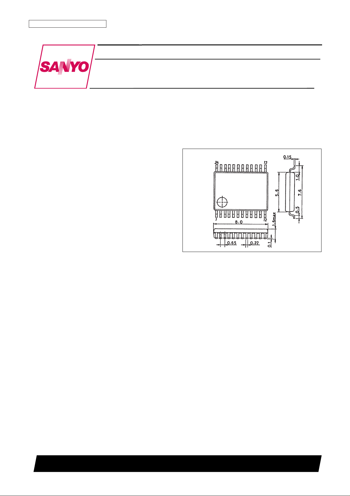
Package Dimensions
unit: mm
3175A-SSOP24
SANYO: SSOP24
[LC89051V]
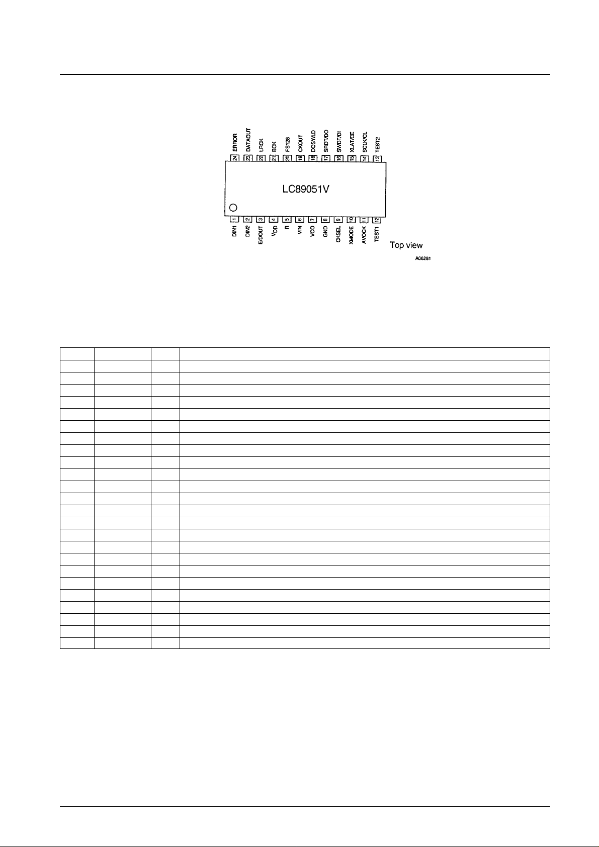
Pin Assignment
Pin Functions
No. 5543-2/15
LC89051V
Pin No. Symbol I/O Description
1 DIN1 I Data input with built-in amplifier (for coaxial or optical module input)
2 DIN2 I Data input (for optical module input)
3 E/DOUT O Emphasis, input bi-phase, and validity flag output
4 V
DD
– Power supply
5 R I VCO gain control input
6 VIN I VCO free-running setting input
7 VCO O PLL low-pass filter setting
8 GND – Ground
9 CKSEL I System clock selection input (384fs or 512fs)
10 XMODE I Reset input
11 AVOCK I PLL error lock avoidance clock input
12 TEST1 I Test input (Must be connected to ground in normal operation)
13 TEST2 I Test input (Must be connected to ground in normal operation)
14 SCLK/CL I Microcontroller interface clock input
15 XLAT/CE I Microcontroller interface latch/chip enable input
16 SWDT/DI I Microcontroller interface write data input
17 SRDT/DO O Microcontroller interface read data output
18 DQSY/LD O Microcontroller interface subcode Q and ID synchronization output
19 CKOUT O VCO clock output (free running, 384fs, or 512fs)
20 FS128 O 128fs clock output
21 BCK O Bit clock output
22 LRCK O L/R clock output (left channel = high, right channel = low)
23 DATAOUT O Audio data output
24 ERROR O PLL lock error mute output
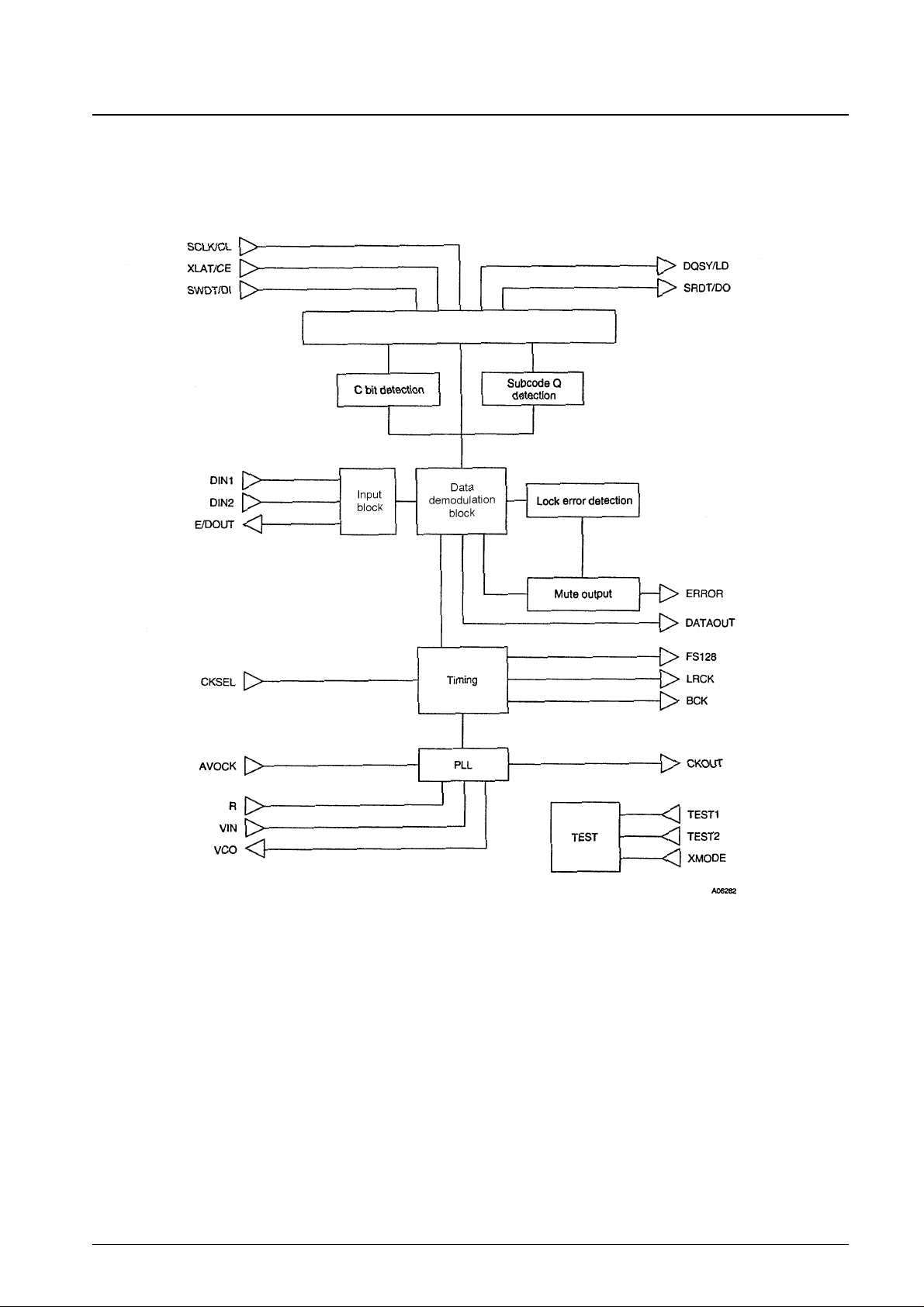
Block Diagram
No. 5543-3/15
LC89051V
Microcontroller interface
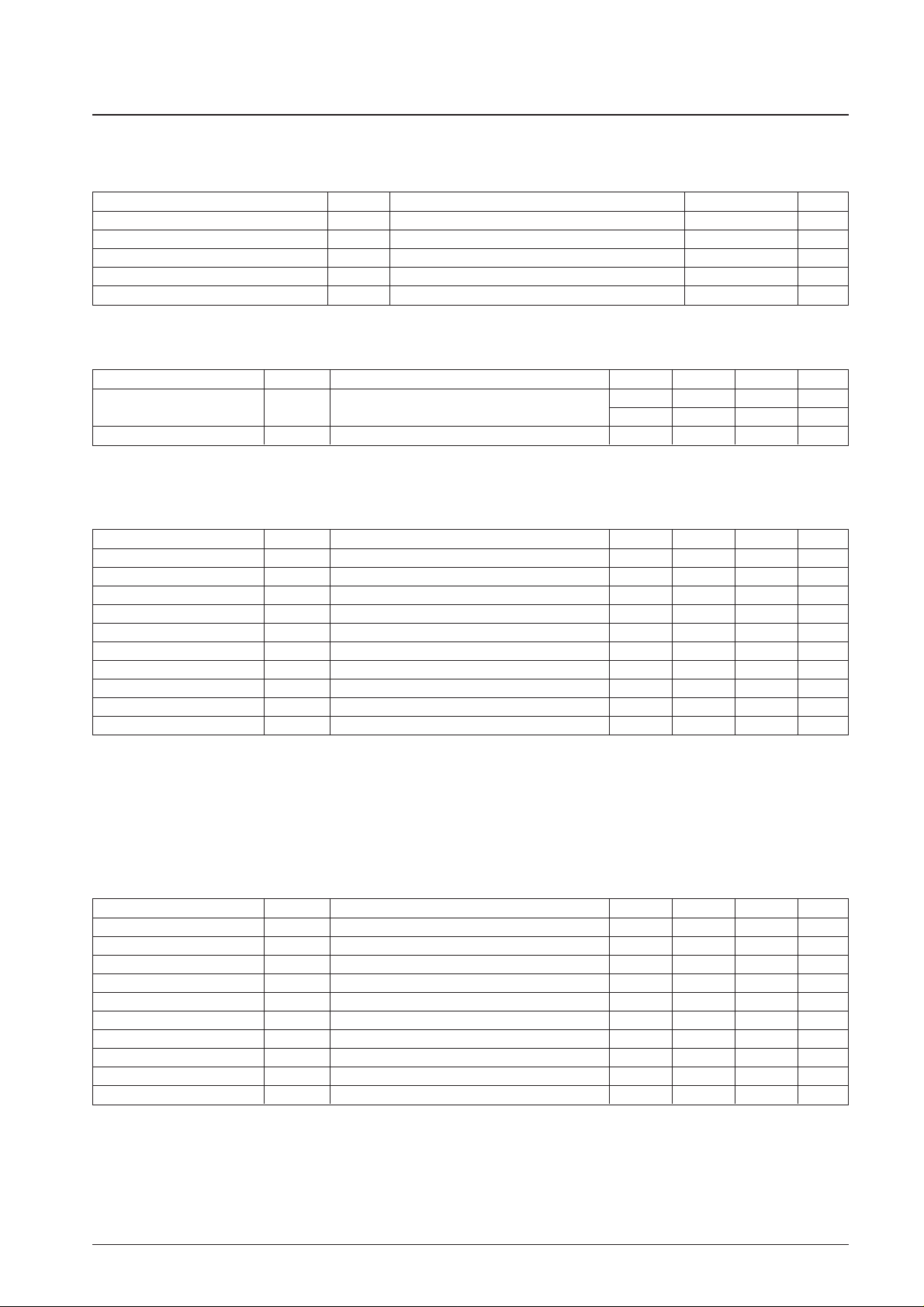
Specifications
Absolute Maximum Ratings
Allowable Operating Ranges
Electrical Characteristics
DC Characteristics (1) at Ta = –30 to +75°C, VDD= 4.5 to 5.5 V, VSS= 0 V
Note: 1. Applies to the CKSEL, AVOCK, TEST1, and TEST2 pins. CMOS levels.
2. Applies to the XMODE, SCLK/CL, XLAT/CE, SWDT/DI pins. CMOS Schmitt inputs.
3. Applies to the DIN2 pin. TTL Schmitt levels.
4. VDD= 5.0 V, Ta = 25°C, input data fs = 96 kHz
5. Measured before the DIN1 pin input capacitor.
DC Characteristics (2) at Ta = –30 to +75°C, VDD= 3.0 to 3.6 V, VSS= 0 V
Note: 6. Applies to the CKSEL, AVOCK, TEST1, and TEST2 pins. CMOS levels.
7. Applies to the XMODE, SCLK/CL, XLAT/CE, SWDT/DI pins. CMOS Schmitt inputs.
8. Applies to the DIN2 pin. TTL Schmitt levels.
9. VDD= 3.3 V, Ta = 25°C, input data fs = 48 kHz
10. Measured before the DIN1 pin input capacitor.
No. 5543-4/15
LC89051V
Parameter Symbol Conditions Ratings Unit
Supply voltage V
DD
–0.3 to +7.0 V
I/O voltages V
I
, V
O
–0.3 to VDD+ 0.3 V
I/O current I
I
, I
O
±20 mA
Operating temperature Topr –30 to +75 °C
Storage temperature Tstg –55 to +125 °C
Parameter Symbol Conditions min typ max Unit
Supply voltage V
DD
3.0 5.0 5.5 V
(3.3)
Operating temperature T
OPR
–30 +75 C°
Parameter Symbol Conditions min typ max Unit
Input high-level voltage V
IH
1 *1 0.7 V
DD
VDD+ 0.3 V
Input low-level voltage V
IL
1 *1 –0.3 0.3 V
DD
V
Input high-level voltage V
IH
2 *2 0.8 V
DD
VDD+ 0.3 V
Input low-level voltage V
IL
2 *2 –0.3 0.2 V
DD
V
Input high-level voltage V
IH
3 *3 2.5 VDD+ 0.3 V
Input low-level voltage V
IL
3 *3 –0.3 +0.6 V
Output high-level voltage V
OHIOH
= –4 mA V
DD
– 2.1 V
Output low-level voltage V
OL
IOL= 4 mA 0.4 V
Current drain I
DD
*4 20 mA
Input amplitude Vpp *5 0.4 V
DD
+ 0.3 V
Parameter Symbol Conditions min typ max Unit
Input high-level voltage V
IH
1 *6 0.7 V
DD
VDD+ 0.3 V
Input low-level voltage V
IL
1 *6 –0.3 0.2 V
DD
V
Input high-level voltage V
IH
2 *7 0.75 V
DD
VDD+ 0.3 V
Input low-level voltage V
IL
2 *7 –0.3 0.15 V
DD
V
Input high-level voltage V
IH
3 *8 2.4 VDD+ 0.3 V
Input low-level voltage V
IL
3 *8 –0.3 +0.3 V
Output high-level voltage V
OHIOH
= –2 mA V
DD
– 0.8 V
Output low-level voltage V
OL
IOL= 2 mA 0.4 V
Current drain I
DD
*9 10 mA
Input amplitude Vpp *10 0.4 V
DD
+ 0.3 V
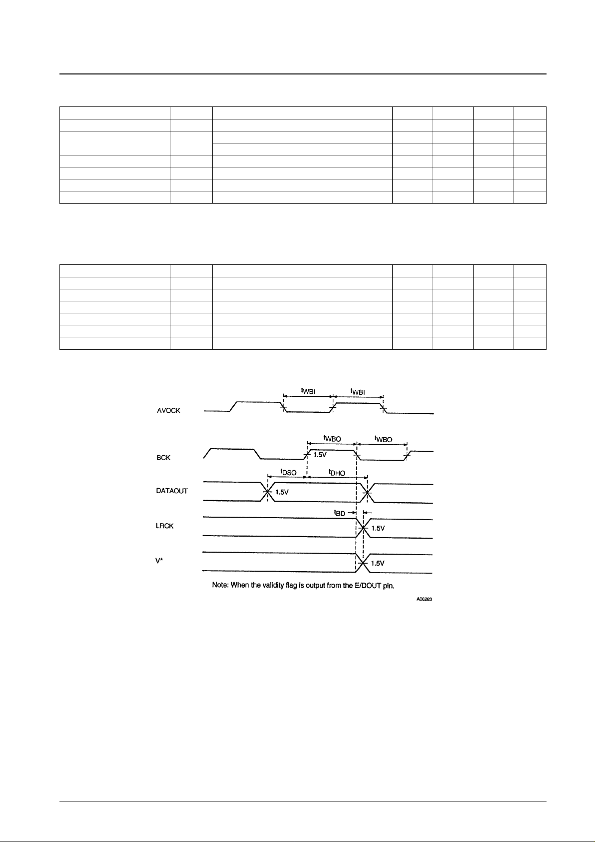
AC Characteristics (Normal Mode) at Ta = –30 to +75°C, VDD= 3.0 to 5.5 V
Note: 11.Ta = 25°C, VDD= 3.3 V, with the circuit constants for standard speed operation in the sample application circuit.
12.Ta = 25°C, V
DD
= 5.0 V, with the circuit constants for standard speed operation in the sample application circuit.
AC Characteristics (Double Speed Mode) at Ta = –30 to +75°C, VDD= 4.5 to 5.5 V
Note: 13.Ta = 25°C, VDD= 5.0 V, with the circuit constants for 2× speed operation in the sample application circuit.
No. 5543-5/15
LC89051V
Parameter Symbol Conditions min typ max Unit
AVOCK input pulse width t
WBI
10 µs
VCO free-running frequency f
VCO
*11 50 MHz
*12 75 MHz
BCK output pulse width t
WBO
fs = 48 kHz 160 ns
Output data setup time t
DSO
80 ns
Output data hold time t
DHO
80 ns
Output delay t
BD
–10 0 +10 ns
Parameter Symbol Conditions min typ max Unit
AVOCK input pulse width t
WBI
10 µs
VCO free-running frequency f
VCO
*13 80 MHz
BCK output pulse width t
WBO
fs = 96 kHz 80 ns
Output data setup time t
DSO
40 ns
Output data hold time t
DHO
40 ns
Output delay t
BD
–10 0 +10 ns
 Loading...