

Page 1
Ordering number : EN4333A
O2494TH VL-0947, 0948/D0392HK No. 4333-1/14
Overview
The LC8902 and LC8902Q are receiver LSIs for
applications in which data is transmitted between digital
audio equipment in the EIAJ format. These LSIs
synchronize with the input signal and demodulate that
signal to a regular format signal.
Features
• Built-in PLL circuit synchronizes with the input EIAJ
format signal.
• Microcomputer interface receives mode settings and
outputs fs codes, copy information, and category codes.
• Supports both 384 fs and 512 fs system clocks
(selectable) and provides 256 fs, 128 fs, BCLK and
LRCK clock outputs.
• Can operate in either digital source mode or analog
source mode.
• User bit CD subcode interface
• DIP42S and QIP44M packages
• Si gate CMOS process, single 5 V power supply
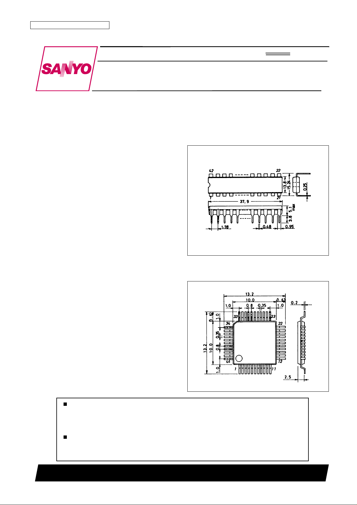
Package Dimensions
unit: mm
3025B-DIP42S
unit: mm
3148-QFP44MA
SANYO: DIP42S
[LC8902]
SANYO: QIP44MA
[LC8902Q]
LC8902, 8902Q
SANYO Electric Co.,Ltd. Semiconductor Bussiness Headquarters
TOKYO OFFICE Tokyo Bldg., 1-10, 1 Chome, Ueno, Taito-ku, TOKYO, 110-8534 JAPAN
Digital Audio Interface Receiver
CMOS LSI
Any and all SANYO products described or contained herein do not have specifications that can handle
applications that require extremely high levels of reliability, such as life-support systems, aircraft’s
control systems, or other applications whose failure can be reasonably expected to result in serious
physical and/or material damage. Consult with your SANYO representative nearest you before using
any SANYO products described or contained herein in such applications.
SANYO assumes no responsibility for equipment failures that result from using products at values that
exceed, even momentarily, rated values (such as maximum ratings, operating condition ranges, or other
parameters) listed in products specifications of any and all SANYO products described or contained
herein.
Page 2
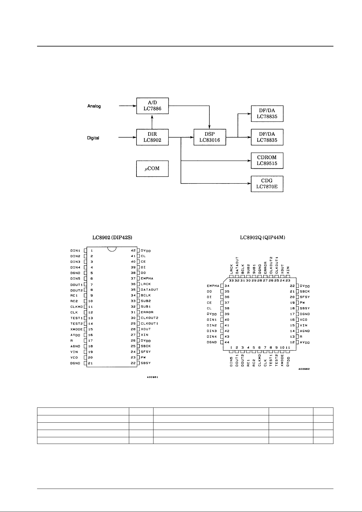
Application Usage Overview Diagram
When both digital source mode and analog source mode are used
Digital source mode: EIAJ CP-1201 format data reception mode
Analog source mode: Analog data is received and converted to digital for signal processing.
This figure shows an example of a structure using the LC8902/Q. In analog source mode the only function of the
LC8902/Q is to provide control clocks.
Pin Assignments
Specifications
Absolute Maximum Ratings at Ta = 25°C
No. 4333-2/14
LC8902, 8902Q
Parameter Symbol Conditions Ratings Unit
Maximum supply voltage V
DD
max –0.3 to +7.0 V
Maximum I/O voltages V
I·VO
max –0.3 to VDD+ 0.3 V
Operating temperature Topr –30 to +75 °C
Storage temperature Tstg –55 to +125 °C
Top view Top view
Page 3
Allowable Operating Ranges
DC Characteristics at Ta = –30 to +75°C, V
DD
= 4.5 to 5.5 V
Note: 1. Input pins other than data input pins DIN1, DIN2, DIN3, DIN4 and XMODE. TTL compatible.
2. The XIN pin. CMOS compatible.
3. The XMODE and RC1 pins. CMOS Schmitt inputs.
4. At Ta = 25°C, V
DD
= 5.0 V, and for an input data fs of 48 kHz.
5. The condition prior to the capacitors on the DIN1, DIN2, DIN3 and DIN4 input pins.
AC Characteristics at Ta = –30 to +75°C, VDD= 4.5 to 5.5 V
Note: 6. For an input data fs of 48 kHz, with a 30 pF load capacitance on each pin.
No. 4333-3/14
LC8902, 8902Q
Parameter Symbol Conditions min typ max Unit
Supply voltage V
DD
4.5 5.0 5.5 V
Operating temperature Topg –30 +75 °C
Parameter Symbol Conditions min typ max Unit
Input high level voltage V
IH
1 *1 2.2 VDD+ 0.3 V
Input low level voltage V
IL
1 *1 –0.3 +0.8 V
Input high level voltage V
IH
2 *2 0.7 V
DD
VDD+ 0.3 V
Input low level voltage V
IL
2 *2 –0.3 +0.3 V
DD
V
Input high level voltage V
IH
3 *3 0.8 V
DD
VDD+ 0.3 V
Input low level voltage V
IL
3 *3 –0.3 +0.2 V
DD
V
Output high level voltage V
OHIOH
= –1 µA VDD– 0.05 V
Output low level voltage V
OLIOL
= 1 µA VSS+ 0.05 V
Current drain I
DD
*4102030mA
Input amplitude V
PP
*5 0.4 VDD+ 0.3 V
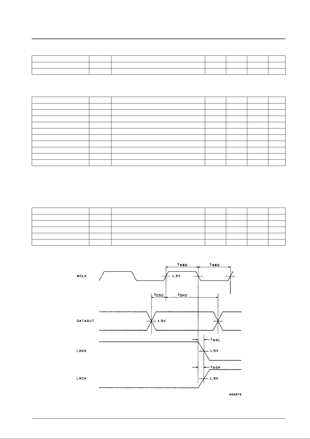
Parameter Symbol Conditions min typ max Unit
Output pulse width t
WBO
*6 160 ns
Output setup time t
DSO
80 ns
Output data hold time t
DHO
80 ns
Output delay (high) t
bdH
–10 0 +10 ns
Output delay (low) t
bdL
–10 0 +10 ns
Page 4
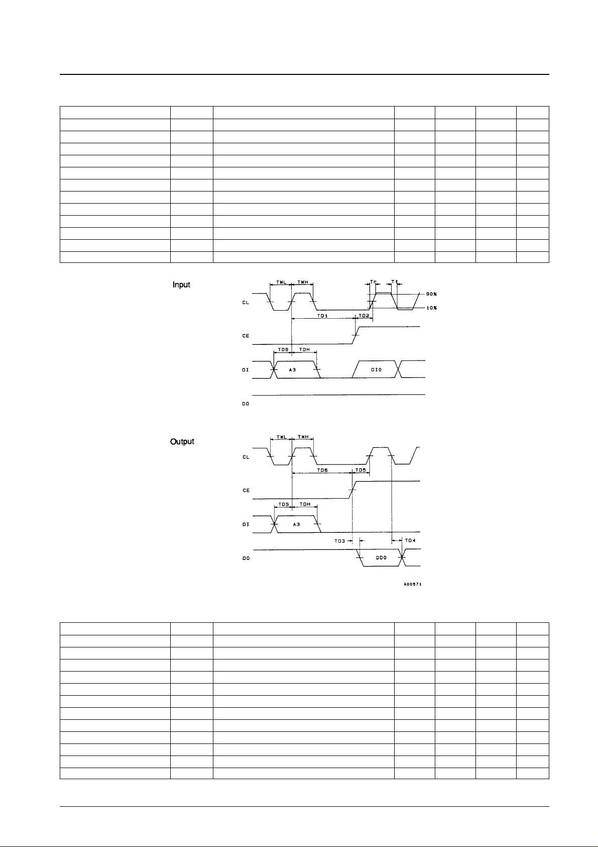
Microcomputer Interface Block AC Characteristics at Ta = –30 to +75°C, VDD= 4.5 to 5.5 V
CD Subcode Interface Block AC Characteristics at Ta = –30 to +75°C, V
DD
= 4.5 to 5.5 V
Note: Assumes that the load capacitance on each output pin is 30 pF.
No. 4333-4/14
LC8902, 8902Q
Parameter Symbol Conditions min typ max Unit
CL low level pulse width TWL 100 ns
CL high level pulse width TWH 100 ns
Data setup time TDS 50 ns
Data hold time TDH 50 ns
CL rise time Tr CL, CE, DI 30 ns
CL fall time Tf CL, CE, DI 30 ns
CE delay time TD1 1.0 µs
CL delay time TD2 50 ns
Data delay time TD3 With a 30 pF load capacitance 25 ns
CL, data delay time TD4 With a 30 pF load capacitance 50 ns
CL delay time TD5 100 ns
CL, CE delay time TD6 1.0 µs
Parameter Symbol Conditions min typ max Unit
SBSY block frequency tB 12.0 13.3 14.7 ms
SBSY pulse width tBW *7 110 µs
SFSY frame frequency tF *8 90 136 165 µs
SFSY high level pulse width tFHW 4 µs
SFSY low level pulse width tFLW 1.5 µs
SBCK high level pulse width tCHW *9 2.0 4.0 5.0 µs
SBCK low level pulse width tCLW *9 2.0 4.0 5.0 µs
SBCK rise time trC 30 ns
SBCK fall time tfC 30 ns
SBCK delay time tCD *9102030µs
P data access tPAC 310µs
Data hold time tHD 0 µs
Page 5
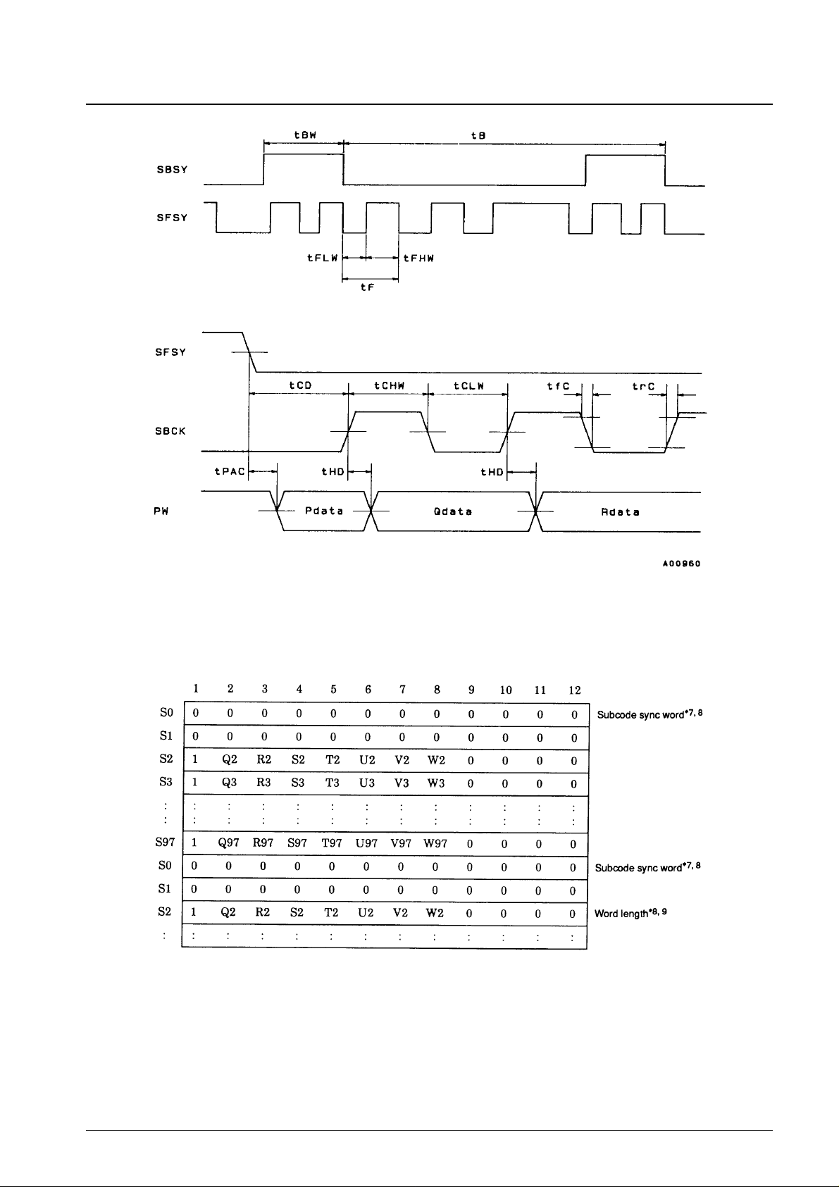
The LC8902/Q uses the subcode synchronization word and the start bit in the user bits for subcode interface system
timing extraction. Therefore, SBSY and SFSY change depending on that timing. Keep the following notes on user bit
transfer in mind when using the values of tBW, tF, tCHW and tCD within the specifications described above. Basically,
user bit transfers must follow the table shown here.
Note: 7. Subcode synchronization is taken as a block synchronization section (the start of a block) when a minimum of 22 consecutive data bits are zero.
8. The frame sync signal S0 period is 90.7 µs. The S1 period also has a minimum value of 90.7 µs (when there are 22 consecutive zero data bits),
depending on the subcode sync word period.
9. When the shortest user data word length is used, the SBCK signal delay (tHD) and pulse widths (tCHW and tCLW) must be set at or below their
typical values.
No. 4333-5/14
LC8902, 8902Q
Page 6

Pin Functions
No. 4333-6/14
LC8902, 8902Q
Pin No.
Symbol I/O Function
QIP DIP
1 6 DIN5 I Data input. There is no built-in amplifier on this pin.
2 7 DOUT1 O
Data outputs
3 8 DOUT2 O
4 9 RC1 I
RC oscillator input
This circuit generates a clock used to detect incorrect PLL locking and to reset the PLL system.
RC oscillator output
5 10 RC2 O This pin outputs a clock with a frequency of about 40 kHz when the component values specified in the sample
application circuit are used.
6 11 CLKMD I CLKOUT2 output clock switching: Low = 256 fs, high = 128 fs
7 12 CLK I Clock mode switching: Low = 384 fs, high = 512 fs
8 13 TEST1 I
Test pin (Should be tied low in normal operation.)
9 14 TEST2 I
10 15 XMODE I Used to start system operation after power is applied.
11 — DV
DD
Digital power supply
12 16 AV
DD
Analog power supply
13 17 R I VCO oscillator band adjustment
14 18 AGND Analog ground
15 19 VIN I VCO free-running setting
16 20 VCO O PLL low-pass filter
17 21 DGND Digital ground
18 22 SBSY O Subcode interface block sync signal
19 23 PW O Subcode interface data output
20 24 SFSY O Subcode interface frame sync signal
21 25 SBCK I Subcode interface bit clock input
22 26 DV
DD
Digital power supply
23 27 XIN I Crystal oscillator input
24 28 XOUT O Crystal oscillator output
25 29 CLK OUT1 O Crystal oscillator and VCO clock output
26 30 CLK OUT2 O 256 fs and 128 fs clock output
27 31 ERROR O Error mute signal output
28 — DGND Digital ground
29 32 SUB1 O
Sampling frequency output
30 33 SUB2 O
31 34 BCLK O Bit clock output
32 35 DATA OUT O Audio data output
33 36 LRCK O Left/right clock output (High = left, low = right)
34 37 EMPHA O High = emphasis on, low = emphasis off. Outputs a low level in analog mode.
35 38 DO O Microprocessor interface output
36 39 DI I Microprocessor interface input
37 40 CE I Microprocessor interface chip enable input
38 41 CL I Microprocessor interface clock input
39 42 DV
DD
Digital power supply
40 1 DIN1 I
41 2 DIN2 I
Data inputs with built-in amplifiers
42 3 DIN3 I
43 4 DIN4 I
44 5 DGND Digital ground
Page 7

Block Diagram
Clock Modes
The LC8902/Q CLKOUT1 and CLKOUT2 output clock modes are selected by the CLK and CLKMD pins according to
the table.
Note: * When the CLK pin is low, the 256 fs clock duty has a high to low ratio of 2:1.
No. 4333-7/14
LC8902, 8902Q
CLK CLK OUT1
L 384 fs clock output
H 512 fs clock output
CLK MD CLK OUT2
L 256 fs clock output*
H 128 fs clock output
Page 8

Microcomputer Interface
The microcomputer interface is used for specifying the data input pin, for setting the output data format, and for
specifying subcode output, system stop, and analog source mode. The figure shows the interface I/O formats.
Microcomputer Interface Formats
Address
The bits B0 to A3 in the format figure are the address. There are two addresses allocated to the LC8902/Q, one for input
and one for output. The microprocessor must specify the input address to input data and the output address to output data.
Address Code
Microcomputer Interface Input
1. Input pin settings
The DIN1 to DIN4 data input pins have built-in amplifiers and can accept signals with levels of about 400 mVp-p.
DIN5 is a special-purpose input pin for optical input.
The data input system multiplexer is controlled by inputs from the microcomputer interface. The table shows the
relationship between the code in bits I5 to I13 in the microcomputer interface format and the data demodulation
outputs DOUT1 and DOUT2.
No. 4333-8/14
LC8902, 8902Q
Mode B0 B1 B2 B3 A0 A1 A2 A3
Data input H L H L L H H L
Data output L H H L L H H L
Page 9

Note: Setting the data demodulation input code to one of the XSYS settings switches the system clock from the VCO to the crystal oscillator and sets
the LC8902/Q to analog source mode. Selecting one of the input pins once again sets the LC8902/Q to digital source mode and PLL operation.
2. Data output mode setting
There are two data output modes: 16-bit MSB first and 20-bit MSB first. These are selected by the bit I14 code.
3. System stop
The operation of both the VCO and the crystal oscillator can be stopped, thus stopping the whole LC8902/Q system,
by setting the bit I4 code as shown in the table.
The values of the bits I4 to I14 are all initialized to low immediately after the XMODE pin goes from low to high.
Since bits I0 to I3 and I15 are not used, their initial values are undefined.
Microcomputer Interface Output
Bits D0 to D15 in the microcomputer interface output format have the following meanings.
Interpretation of the D1 and D2 bits
Note: 1. The “#1” value indicates either a PLL lock error or analog source mode. In these states the data is cleared and bits D0 and D3 to D15 are all set to low.
2. D1 and D2 are in the “#1” state in the initial values of the codes immediately after the XMODE pin goes from low to high. All other codes are set to low.
3. The interval between one microcomputer data read out operation and the next must be 6 ms or longer.
No. 4333-9/14
LC8902, 8902Q
I5 LH LHLHLH
I6 L LHHLLHH
I7 LLLLHHHH
Data demodulation input DIN1 DIN2 DIN3 DIN4 DIN5 XSYS XSYS XSYS
I8 LH LHLHLH
I9 L LHHLLHH
I10 LLLLHHHH
DOUT1 DIN1 DIN2 DIN3 DIN4 DIN5 GND GND GND
I11 LHLH LHLH
I12 LL HH LL HH
I13 LLLLHHHH
DOUT2 DIN1 DIN2 DIN3 DIN4 DIN5 GND GND GND
I14 L H
Data output mode 16-bit MSB first 20-bit MSB first
I4 L H
— System operation System stop
Bit Function
D0 Invalid bit. Always output as a low level.
D1 Indicates the sample frequency.
D2 Corresponds to the fs external output pin.
D3
Indicates the state of the copy flag.
High = copy enabled, low = copy protect
D4 Outputs the first bit of the channel status bits.
D5 to D12 These pins output the channel status 8-bit category codes serially.
D13 to D15 Invalid bits. Always output as low levels.
Sampling frequency 32 kHz 44.1 kHz 48 kHz #1
D1 H L L H
D2 HLHL
Page 10

FS Output Code
The SUB1 and SUB2 pins indicate the input data sampling frequency.
Note: The “#1” values indicates PLL lock error or analog source mode. When SUB1 and SUB2 have these values, the DATAOUT and EMPHA pins will
output low levels.
CD Subcode Interface
The LC8902/Q uses the SFSY, SBCK, PW and SBSY pins to output the CD subcode data. This data is the user bits that
were transferred according to the CP-1201 interface format and converted to a format that conforms to the CP-2401
interface format. The timing is shown in the figures.
The timing of the rising and falling edges of the SFSY signal is changed according to the timing of the start bits in the
input data user bits as shown in the figure.
No. 4333-10/14
LC8902, 8902Q
Sampling frequency 32 kHz 44.1 kHz 48 kHz #1
SUB1 H L L H
SUB2 H L H L
Page 11

Errors
1. ERROR pin: This pin goes high when there are errors in the input data or when the PLL circuit is unlocked. When
data demodulation returns to normal, the high level is held for about 200 to 300 ms and then the ERROR pin goes
low. This time is inversely proportional to the fs of the input data.
2. Data processing when an error occurs: The table lists the data processing performed when an error occurs.
Note: Preamble detection is used to recognize PLL lock errors.
Analog Source Mode
The LC8902/Q switches to analog source in the following two cases.
1. When analog source mode is selected by the data sent over the microcomputer interface
2. When there is no signal on the input pin selected for data demodulation
In analog source mode, the clock that runs the whole system is supplied by the crystal oscillator clock and the PLL
circuit and data demodulation are stopped. The BCLK, LRCK, CLK, OUT1 and CLKOUT2 clocks are output.
The output pins function as follows in analog source mode.
• DOUT1, DOUT2
Data specified through the microcomputer interface is output.
• ERROR
The lock error state high level is output.
• SUB1, SUB2
The “#1” lock error state code is output.
• DATAOUT
The lock error state low level is output.
• EMPHA
The lock error state low level is output.
• Microcomputer interface codes
Input codes: The code values set through the microcomputer interface are retained.
Output codes: Values identical to those for a PLL lock error are output.
Crystal Oscillator
1. The presence or absence of data is determined by an internal detection circuit. This circuit operates on either the
VCO or the crystal oscillator clock. When power is first applied, the clock is supplied from the VCO, and the
LC8902/Q switches to the crystal oscillator if a no data state is detected. Here, if a clock signal was not supplied
from the crystal oscillator after a no data state is detected, the whole system would stop and remain in the stopped
state, since the detection circuit would not operate even if data were supplied.
2. The XIN and XOUT pins include a built-in oscillator amplifier circuit, and take on the following states when a
crystal oscillator is connected.
Note: * The XIN pin is pulled-up internally when the LC8902/Q is in the data present state.
No. 4333-11/14
LC8902, 8902Q
Error Type Audio Output Data FS Output Code
Up to 8 consecutive parity errors Previous data value output Retained
Nine or more consecutive
Data with the value zero is output. Retained
parity errors
PLL lock error Data with the value zero is output.
Data is cleared and the “#1” state is
indicated.
Pin Data Present* Data Absent
XIN High Accepts crystal oscillator input.
XOUT Low Outputs the inverted state of the XIN pin.
Page 12

XMODE
The XMODE pin resets the LC8902/Q system. The LC8902/Q will start to function normally if a high level is applied to
this pin after the power supply voltage rises above a value of at least 4.5 V.
1. Once the LC8902/Q is operating, the system will be reset if a low level is applied once again to the XMODE pin.
2. This IC can be used without using the microcomputer interface by tying the CE, CL and DI microcomputer interface
input pins low and using D1 as the data input pin. This technique can be used as a simplified method for product
evaluation.
Data Output Timing
The figures show the data output timing.
1. Data is output in synchronization with the falling edge of the BCLK signal.
2. Data, BCLK and LRCK are output in synchronization with the rising edge of the 256 fs clock.
3. The data output timings for 20-bit MSB first and 16-bit MSB first output are shown in the timing charts.
Timing Chart
No. 4333-12/14
LC8902, 8902Q
Page 13

Sample Application Circuit
Circuit Constants
No. 4333-13/14
LC8902, 8902Q
Item Symbol Value Item Symbol Value
R1 33 kΩ C1 1000 pF
R2 10 kΩ C2 10 to 100 µF
R3 24 kΩ C3 0.1 µF
Resistors
R4 5.6 kΩ
Capacitors
C4 0.01 µF
R5 5.6 kΩ C5 10 to 47 pF
R6 120 to 150 Ω C6 10 to 47 pF
R7 200 Ω
R8 200 kΩ
Page 14

PS No. 4333-14/14
LC8902, 8902Q
Input Pin Application Circuits
This catalog provides information as of August, 1998. Specifications and information herein are subject to
change without notice.
Specifications of any and all SANYO products described or contained herein stipulate the performance,
characteristics, and functions of the described products in the independent state, and are not guarantees
of the performance, characteristics, and functions of the described products as mounted in the customer’s
products or equipment. To verify symptoms and states that cannot be evaluated in an independent device,
the customer should always evaluate and test devices mounted in the customer’s products or equipment.
SANYO Electric Co., Ltd. strives to supply high-quality high-reliability products. However, any and all
semiconductor products fail with some probability. It is possible that these probabilistic failures could
give rise to accidents or events that could endanger human lives, that could give rise to smoke or fire,
or that could cause damage to other property. When designing equipment, adopt safety measures so
that these kinds of accidents or events cannot occur. Such measures include but are not limited to protective
circuits and error prevention circuits for safe design, redundant design, and structural design.
In the event that any and all SANYO products described or contained herein fall under strategic
products (including services) controlled under the Foreign Exchange and Foreign Trade Control Law of
Japan, such products must not be exported without obtaining export license from the Ministry of
International Trade and Industry in accordance with the above law.
No part of this publication may be reproduced or transmitted in any form or by any means, electronic or
mechanical, including photocopying and recording, or any information storage or retrieval system,
or otherwise, without the prior written permission of SANYO Electric Co., Ltd.
Any and all information described or contained herein are subject to change without notice due to
product/technology improvement, etc. When designing equipment, refer to the “Delivery Specification”
for the SANYO product that you intend to use.
Information (including circuit diagrams and circuit parameters) herein is for example only; it is not
guaranteed for volume production. SANYO believes information herein is accurate and reliable, but
no guarantees are made or implied regarding its use or any infringements of intellectual property rights
or other rights of third parties.
 Loading...