

Page 1
Ordering number : ENN*6686
CMOS IC
LC86F1216A
8-Bit Single Chip Microcontroller with
16K-Byte ROM and 1220-Byte RAM On Chip
Preliminary
Overview
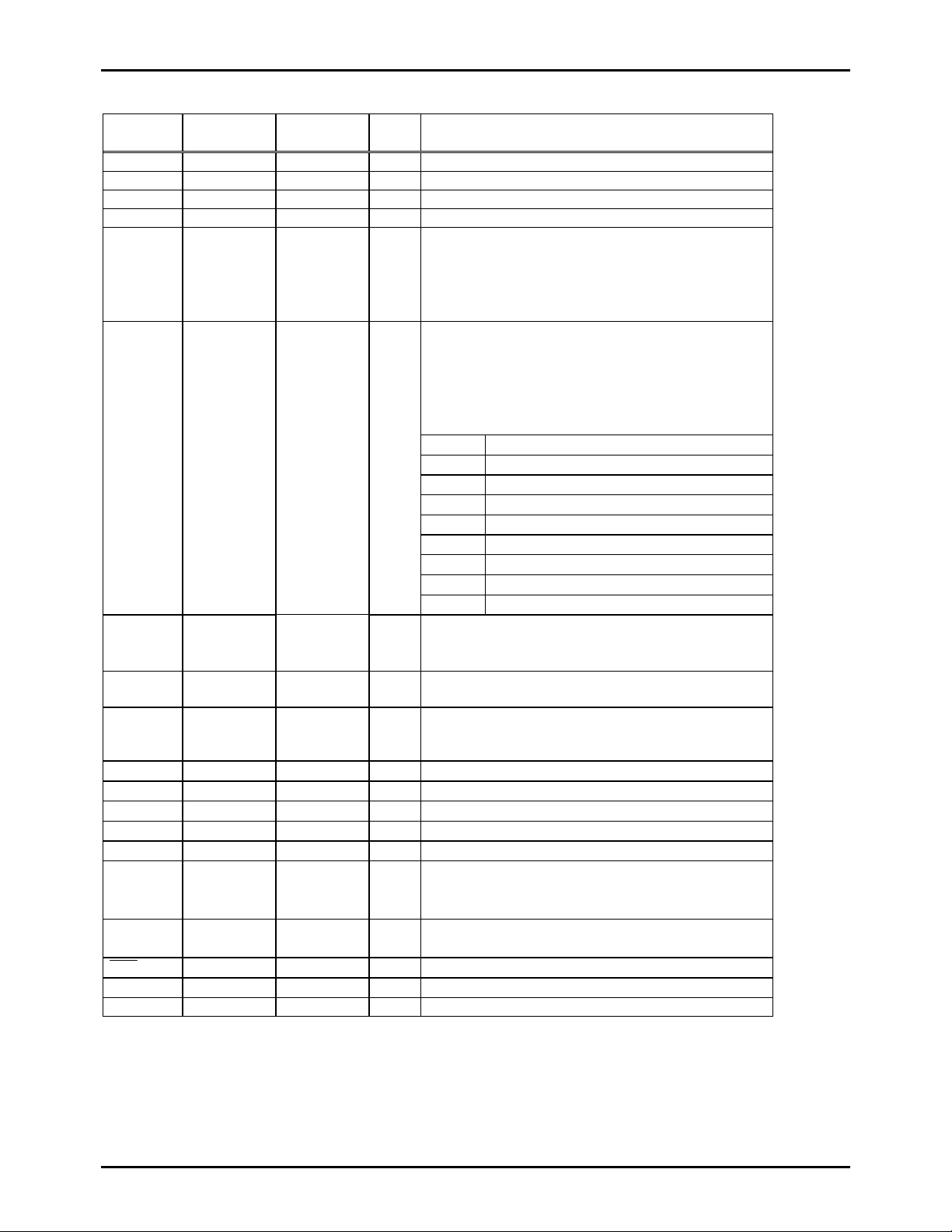
The LC86F1216A is an 8-bit single chip microcontroller with the following on-chip functional blocks:
- CPU: Operable at a minimum bus cycle time of 0.5µs
- On-chip Flash EEPROM capacity: 144 Kbytes
- On-chip RAM capacity: 1222 bytes
- Dot matrix liquid crystal display controller / driver
- 16-bit timer/counter (or tw o chan nels × 8-bit timer)
- 16-bit timer/PWM (or two channels × 8-bit timer)
- Serial interface circuit
All of the above functions are fabricated on a single chip.
Features
(1)Flash EEPROM: 64K × 8 bits: (program/data area) + 64K × 8 bits (data area)
16K × 8 bits: (program area)
(2) Mask ROM: 4K × 8 bits: (4K: BIOS program area)
(3) Random Access Memory (RAM): 512 × 8 bits (calculation area) + 512 × 8 bits
198
(4) Bus Cycle Time
Note: Bus cycle time means cycle time of reading ROM. OCR7: Bit 7 of the oscillation control register
(5) Ports
- Input / Output Ports: 2 ports (16 terminals)
- Input port: 1 port (4 terminals)
8 bits (display area)
×
Bus Cycle Time
0.5µs 1.0µs Ceramic 6MHz OCR7 = 1
3.8µs 7.5µs External RC 600kHz OCR7 = 1
93µs 183µs X’tal 32.768kHz
Cycle Time System Clock Oscillation Oscillation Frequency Voltage Notes
3.15–3.85V
OCR7 = 1
Ver.1.02
11800
91400 RM (IM) Ohsawa No.6686-1/21
Page 2

LC86F1216A
(6) Dot matrix liquid crystal display controller / driver
- Display duty: 1/33 duty
- Display bias: 1/5 bias
- LCD power supply (max. 6V)
- LCD driver (max. 1584 dots capability)
Common output ports: 33 ports
Segment output ports: 48 ports
- Externally boosted clock
(7) Serial interfaces
- Synchronous 8-bit serial interface × 2 (with 8-bit baud rate generator)
(8) Timers
- Timer 0 (T0H/T0L)
16-bit timer/counter
- Timer 1 (T1H/T1L)
16-bit timer/PWM
(9) Interrupts
- 13 sources 10 vectored interrupts
(10) Sub-routine stack level
- A maximum of 128 levels (stack is built in the internal RAM)
(11) 3 oscillation circuits
- External RC oscillation circuit / CF oscillation circuit / X’tal oscillation circuit
(12) Power voltage
- VDD = 3.15V – 3.85V
(13) Shipping form
- Chip or SQFP144
(14) Flash memory
- Erasing block unit size: 128 bytes
- Erasing / writing voltage range: 3.15V – 5.5V
- Maximum number of erase-write cycle: 50,000 times (Ta = +25°C) (with memory management program)
Note
The microcontroller will malfunction if the power supply voltage is less than the specified operable supply voltage. To
prevent a malfunction, the low voltage detect circuit should be connected externally, and the volta ge should always be set
to the proper level. If the power supply voltage becomes lower than the voltage which is detected by the low voltage detect
reset IC, then the m icrocont roller should be reset to restore stable opera tion. Use t he low volta ge detect re set IC which
detects the lowest specification voltage of the power supply.
We cannot ensure the integrity of the block data, if the microcontroller is reset while writing to the flash memory.
Therefore, in such a case, we recommend disabling any flash writing operation by user's program when the voltage
decreases to a level just above the voltage which is detected by the low voltage detect reset IC.
No.6686-2/21
Page 3
Pin Assignment
T
K
SQFP144
NC
S7
S6
S5/A11
S4/A9
S3/A8
S2/A13
S1/A14
WE
VDD
EP
F/M_SEL
C1/A17
C2/A16
C3/A15
C4/A12
C5/A7
C6/A6
C7/A5
C8/A4
C9
C10
C11
C12
C13
C14
C15
C16
VSS
V1
V2
V3
V4
V5
VLCD
NC
108 105 100 98 97 96 95 94 93 92 91 90 89 88 87 86 85 84 83 82 81 80 79 78 77 76 75 74 73
110
111
112
113
114
115
116
117
118
119
120
121
122
123
124
125
126
127
128
129
130
131
132
133
134
135
136
137
138
139
140
141
142
143
144
12345678910 11 12 13 14 15 16 17 18 19 20 21 22 23 24 25 26 27 28 29 30 31 32 33 34 35 36
Package Dimension
(unit : mm)
3214
LC86F1216A
NC
S8
S9
S10
S11
S12
S13
S14
S15
S16
S17
S18
S19
S20
S21
S22
S23
S24
S25
S26
S27
S28
S29
S30
S31
S32
S33
S34
S35
S36
S37
S38
S39
S40
S41
NC
72
71
70
69
68
67
66
65
64
63
62
61
60
59
58
57
56
LC86F1216A
RES
XT1
XT2
VDD
NCTE
NCEX
SUPCL
RCIN
NCT2
NCTD
NCTC
NCT1
TEST1
RCOUT
TEST2
VDD
VSS
P70
P71
P72
P73
P30
P31
P32
CF1
CF2
VDD
P33
P34/A3
P35/A2
P36/A1
P37/A0
55
54
53
52
51
50
49
48
47
46
45
44
43
42
41
40
39
38
37
NC
P10/DQ0
P11/DQ1
P12/DQ2
NC
S42
S43
S44
S45
S46
S47
S48
C17
C18
C19
C20
C21
C22
C23
C24
C25
C26
C27
C28
C29
C30
C31
C32
C33
OE
A10
CE
P17/DQ7
P16/DQ6
P15/DQ5
P14/DQ4
P13/DQ3
VSS
NC
NC
SANYO : SQFP-144
No.6686-3/21
Page 4
Pad Assignment
K
S7
S6
S5/A11
S4/A9
S3/A8
S2/A13
S1/A14
WE
VDD
EP
F/M_SEL
C1/A17
C2/A16
C3/A15
C4/A12
C5/A7
C6/A6
C7/A5
C8/A4
C9
C10
C11
C12
C13
C14
C15
C16
VSS
V1
V2
V3
V4
V5
VLCD
S8
103
104
105
106
107
108
109
110
111
112
113
114
115
116
117
118
119
120
121
122
123
124
125
126
127
128
129
130
131
132
133
134
135
136
137
1 2 3 4 5 6 7 8 9
NCEXT
SUPCL
LC86F1216A
S9
S10
S11
S12
S13
S14
S15
S16
S17
S18
S19
S20
S21
S22
S23
S24
S25
S26
S27
S28
S29
S30
S31
S32
S33
S34
9998979695949392919089888786858483828180797877767574737271
102
101
100
10
11
12
13
14
15
16
17
18
19
20
21
22
23
24
25
26
27
P70
P71
P72
P73
P30
P31
XT1
VDD
NCTE
RCIN
NCTD
NCT2
NCTC
RCOUT
RES
NCT1
TEST1
TEST2
XT2
CF1
CF2
VSS
VDD
VDD
P32
S35
28
P33
29
P34/A3
S36
30
P35/A2
S37
31
P36/A1
S38
32
P37/A0
S39
33
P10/DQ0
S40
34
P11/DQ1
S41
70
69
68
67
66
65
64
63
62
61
60
59
58
57
56
55
54
53
52
51
50
49
48
47
46
45
44
43
42
41
40
39
38
37
36
35
P12/DQ2
S42
S43
S44
S45
S46
S47
S48
C17
C18
C19
C20
C21
C22
C23
C24
C25
C26
C27
C28
C29
C30
C31
C32
C33
OE
A10
CE
P17/DQ7
P16/DQ6
P15/DQ5
P14/DQ4
P13/DQ3
VSS
VSS
No.6686-4/21
Page 5
LC86F1216A
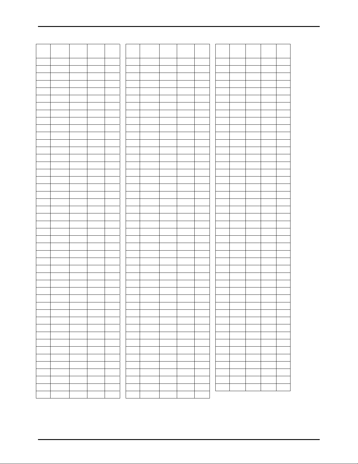
Pad Name and Coordi nates Table
PAD
Pin Name X-cord Y-cord SQFP-
No.
1 NCEXT -2965 -3540 1 47 C32 3333 -698 49 93 S18 -1139 3539 97
2 SUPCLK -2791 -3540 2 48 C31 3333 -524 50 94 S17 -1313 3539 98
3 VDD -2617 -3540 3 49 C30 3333 -350 51 95 S16 -1486 3539 99
4 NCTE -2443 -3540 4 50 C29 3333 -176 52 96 S15 -1660 3539 100
5 NCTD -2269 -3540 5 51 C28 3333 -2 53 97 S14 -1834 3539 101
6 NCTC -2096 -3540 6 52 C27 3333 171 54 98 S13 -2008 3539 102
7 RCOUT -1922 -3540 7 53 C26 3333 345 55 99 S12 -2182 3539 103
8 RCIN -1748 -3540 8 54 C25 3333 519 56 100 S11 -2356 3539 104
9 NCT2 -1574 -3540 9 55 C24 3333 693 57 101 S10 -2530 3539 105
10 NCT1 -1400 -3540 10 56 C23 3333 867 58 102 S9 -2703 3539 106
11 TEST1 -1226 -3540 11 57 C22 3333 1041 59 103 S8 -2877 3539 107
12 TEST2 -1052 -3540 12 58 C21 3333 1215 60 104 S7 -3333 2992 110
13 RES# -879 -3540 13 59 C20 3333 1388 61 105 S6 -3333 2818 111
14 VDD -705 -3540 14 60 C19 3333 1562 62 106 S5/A11 -3333 2644 112
15 XT1 -531 -3540 15 61 C18 3333 1736 63 107 S4/A9 -3333 2470 113
16 XT2 -357 -3540 16 62 C17 3333 1910 64 108 S3/A8 -3333 2296 114
17 VSS -183 -3540 17 63 S48 3333 2084 65 109 S2/A13 -3333 2122 115
18 CF1 -9 -3540 18 64 S47 3333 2258 66 110 S1/A14 -3333 1949 116
19 CF2 165 -3540 19 65 S46 3333 2432 67 111 WE# -3333 1749 117
20 VDD 338 -3540 20 66 S45 3333 2605 68 112 VDD -3333 1549 118
21 P70 512 -3540 21 67 S44 3333 2779 69 113 EP -3333 1375 119
22 P71 686 -3540 22 68 S43 3333 2953 70 114 F/MSEL -3333 1202 120
23 P72 860 -3540 23 69 S42 3333 3127 71 115 C1/A17 -3333 1010 121
24 P73 1034 -3540 24 70 S41 2860 3539 74 116 C2/A16 -3333 836 122
25 P30 1208 -3540 25 71 S40 2686 3539 75 117 C3/A15 -3333 662 123
26 P31 1382 -3540 26 72 S39 2512 3539 76 118 C4/A12 -3333 488 124
27 P32 1556 -3540 27 73 S38 2339 3539 77 119 C5/A7 -3333 314 125
28 P33 1729 -3540 28 74 S37 2165 3539 78 120 C6/A6 -3333 140 126
29 P34/A3 1903 -3540 29 75 S36 1991 3539 79 121 C7/A5 -3333 -34 127
30 P35/A2 2077 -3540 30 76 S35 1817 3539 80 122 C8/A4 -3333 -207 128
31 P36/A1 2251 -3540 31 77 S34 1643 3539 81 123 C9 -3333 -381 129
32 P37/A0 2425 -3540 32 78 S33 1469 3539 82 124 C10 -3333 -555 130
33 P10/DQ0 2599 -3540 33 79 S32 1295 3539 83 125 C11 -3333 -729 131
34 P11/DQ1 2773 -3540 34 80 S31 1122 3539 84 126 C12 -3333 -903 132
35 P12/DQ2 2946 -3540 35 81 S30 948 3539 85 127 C13 -3333 -1077 133
36 VSS 3333 -2756 39 82 S29 774 3539 86 128 C14 -3333 -1251 134
37 VSS 3333 -2582 39 83 S28 600 3539 87 129 C15 -3333 -1425 135
38 P13/DQ3 3333 -2408 40 84 S27 426 3539 88 130 C16 -3333 -1598 136
39 P14/DQ4 3333 -2234 41 85 S26 252 3539 89 131 VSS -3333 -1772 137
40 P15/DQ5 3333 -2061 42 86 S25 78 3539 90 132 V1 -3333 -1946 138
41 P16/DQ6 3333 -1887 43 87 S24 -95 3539 91 133 V2 -3333 -2120 139
42 P17/DQ7 3333 -1713 44 88 S23 -269 3539 92 134 V3 -3333 -2294 140
43 CE# 3333 -1539 45 89 S22 -443 3539 93 135 V4 -3333 -2468 141
44 A10 3333 -1365 46 90 S21 -617 3539 94 136 V5 -3333 -2642 142
45 OE# 3333 -1191 47 91 S20 -791 3539 95 137 VLCD -3333 -2815 143
46 C33 3333 -872 48 92 S19 -965 3539 96
144
PAD
No.
Pin Name X-cord Y-cord SQFP-1
44
PAD
No.
Pin
X-cord Y-cord SQFP-
Name
144
No.6686-5/21
Page 6
LC86F1216A
Terminal Function
Terminal Pin No. Pad No.
VSS 17,39,137 17,36-37,131 - ·Negative power supply
VDD 3,14, 20,118 3,14,20,112 - ·Positive power supply
VLCD 143 137 - ·Positi ve power supply (power supply for LCD driver)
V1-5 138-142 132-136 - ·Power supply for LCD driver
PORT3 25-32 25-32 I/O
PORT1 33-35
40-44
PORT7 21-24 21-24 I
C01-C33 121-136
64-48
S01-S48 116-110
107-74
71-65
SUPCK 2 2 O
CF1 18 18 I
CF2 19 19 O
XT1 15 15 I
XT2 16 16 O
RCIN 8 8 I
RCOUT 7 7 O
RES
TEST1 11 11 TEST2 12 12 - ·Test terminal Leave open circuit.
13 13 I
33-35
38-42
115-130
62-46
110-63 O ·LCD controller
Input/
Output
I/O
O
·8 bit I/O port
(Output fo rmat: CMOS with pu ll-up resistor: P30-P37)
·I/O programmable for each bit individually
·Used for switch input
·Key interrupt input
·8 bit I/O port
(Output format: CMOS: P16, P17
Nch-OD: P10, P11, P12, P13, P14, P15)
(pull-up resistor : P10 - P17)
·I/O programmable for each bit individually
·Other functions
Terminal Serial
P10 Serial OUT0
P11 Serial IN0
P12 Serial Clock0
P13 Serial OUT1
P14 Serial IN1
P15 Serial Clock1
P16 Buzzer output
P17 Timer1 output (PWM output)
·4bit input port (pull-up resistor: P70 - P73)
·External in terrupt function
·Input only
·LCD controller
Common output terminals
Segment output terminals
·Externally boosted clock output terminal
·Input terminal for ceramic resonator
·Output terminal for ceramic resonator
·Input terminal for 32.768kHz X’tal
·Output terminal for 32.768kHz X’tal
·Input terminal for RC oscillation
Connect R between RCIN and RCOUT, and C between
RCIN and VSS.
·Output terminal for RC oscillation
Connect R between RCOUT and RCIN.
·Reset terminal
·Test terminal Leave open circuit.
Function Description
Continued.
No.6686-6/21
Page 7
LC86F1216A
Terminal Pin No. Pad No.
NCT1, NCT2,
NCTC,
NCTD, NCTE
, OE,
CE
WE
EP, A10 119,46 113,44 I ·Memory test terminal Leave open circuit.
F/M_SEL 120 114 I ·Connect to VDD.
NC 36,37,38,
NCEXT 1 1 I ·Test terminal
10,9,
6,5
4
45,47,117 43,45 I ·Memory test terminal Pull up to VDD.
72,73,108,
109,144
10,9
6,5
4
- ·Unused terminal Le ave open circuit.
Input/
Output
- ·Test terminal Leave open circuit.
Connect this ter m inal to VSS.
Function Description
*Initial Port Status
Terminal Input/Output Pull-up Resistor Status
Port1 I Programmable pull-up resistor : OFF
Port3 I Programmable pull-up resistor : OFF
No.6686-7/21
Page 8

System Bl ock Diagram
LC86F1216A
Base Timer
SIO0
Port 1
RAM (buffer)
ADDRESS (512bytes)
Address Register (8bits)
SIO1
CF
RC
X’tal
Clock
Generator
Noise Rejection Filter
Interrupt Control
Standby Control
Bus Interface
Port 7
INT0-3
Timer 0
Timer 1
RAM (512bytes)
IR PLA
Flash EEPROM Control
Flash EEPROM
PC
ROM
ACC
B Register
Display RAM (198bytes)
LCD Controller
LCD Driver
(33 commons×48 segments)
RAR
Stack Pointer
Port 3
EXT Register
C Register
ALU
PSW
No.6686-8/21
Page 9

LC86F1216A
1. Absolute Maximum Ratings at Ta=+25°C, VSS=0V
Parameter Symbol Pins Conditions
Supply voltage VDDMAX VDD -0.3 to +6.0
Input voltage
Input/output
voltage
High
level
output
current
Peak
output
current
Total
output
current
Low
level
output
current
output
current
Total
output
current
Maximum power
consumption
Operating
temperature range
Storage
temperature range
VI(1) Port 71, 72, 73
RES
VI(2) VLCD -0.3 to +6.5
VO(1) C1 to C33
S1 to S48
VO(2) TEST1, TEST2, SUPCK -0.3 to VDD+0.3
VIO(1) Port 1, 3
Port 70
TEST1
IOPH(1) Port 1, 3
TEST1, TEST2, SUPCK
Σ
IOAH(1) Port 3
C1 to C33, S1 to S48
TEST1, TEST2, SUPCK
Σ
IOAH(2) Port 1 Total of all pins -25
IOPL(1) Port 1, 3
TEST1, TEST2, SUPCK
IOPL(2) Port 70 For each pin 15
Σ
IOAL(1) Port 1 Total of all pins 40
Σ
IOAL(2) TEST1, TEST2, SUPCK Total of all pins 40
Σ
IOAL(3) Port 70 Total of all pins 15
Σ
IOAL(4) C1 to C33, S1 to S48 Total of all pins 30
Σ
IOAL(5) Port 70 Total of all pins 15
Pdmax SQFP144
Topr 0 +50
Tstg -55 +125
Ratings
VDD[V] Min. Typ. Max.
Unit
V
-0.3 to VDD+0.3
-0.3 to VLCD+0.3 Output voltage
-0.3 to VDD+0.3
·CMOS output
-4
mA
·For each pin
Total of all pins -25
For each pin 20 Peak
Ta = 0°C to +50°C
400
mW
°
C
No.6686-9/21
Page 10

LC86F1216A
2. Recommended Operating Range at Ta=0°C to +50°C, VSS=0V
Parameter Symbol Pins Conditions
Operating
supply voltage
range
Hold voltage VHD VDD RAM and register
LCD voltage VLCD VLCD 3.15-3.85 VDD 6.0
High level
input voltage
input voltage
Operation
cycle time
VDD(1) VDD
98µs tCYC 400µs
data are kep t i n
HOLD mode.
VIH(1) ·Port 1, 3
·Port 72, 73 (schmitt)
VIH(2) ·P70
Output disable 3.15-3.85 0.7VDD VDD
Output N-ch Tr.: OFF 3.15-3.85 0.7VDD VDD
port input/interrupt
·P71
(schmitt)
RES
VIL(1) ·Port 1, 3
·Port 72, 73 (schmitt)
VIL(2) ·P70
Output disable 3.15-3.85 VSS 0.3VDD Low level
Output N-ch Tr.: OFF 3.15- 3.85 VSS 0.3VDD
port input/interrup t
·P71
(schmitt)
RES
tCYC 3.15-3.85 0.98 400
Ratings
VDD[V] Min. Typ. Max.
3.15 3.85
2.0 3.85
Unit
V
µ
s
No.6686-10/21
Page 11

LC86F1216A
V
3. Electrical Characteristics at Ta=0°C to +50°C, VSS=0V
Parameter Symbol Pins Conditions
High level
input
current
IIH(1) Port 1, 3 ·Output disable
·Pull-up MOS Tr.: OFF
·VIN=VDD (including
OFF state leak current of
output Tr.)
IIH(2) Port 7 without
pull-up MOS Tr.
·Output N-ch Tr.: OFF
·VIN=VDD (including
OFF state leak current of
output Tr.)
Low level
input
current
IIH(3)
IIH(4)
RES
, OE, WE
CE
IIL(1) Port 1,3 ·Output disable
VIN=VDD 3.15–3.85 1
VIN=VDD 3.15–3.85 1
·Pull-up MOS Tr.: OFF
·VIN=VSS (including OFF
state leak current of
output Tr.)
IIL(2) Port 7 without
pull-up MOS Tr.
·Output N-ch Tr.: OFF
·VIN=VSS (including OFF
state leak current of
output Tr.)
IIL(3)
RES
IIL(4) A10, EP, F/M_SEL
, OE, WE
CE
High level
output
voltage
VOH(1) Port 0, 1, 3: CMOS
output
TEST1, TEST2,
VIN=VSS 3.15–3.85 -1
VIN=VSS 3.15–3.85 -1
IOH=-0.1mA 3.15–3.85
SUPCK
Low level
output
voltage
VOL(1) Port 1,3
TEST1, TEST2,
SUPCK
·IOL=1mA
·IOL at any single pin is
not over 1mA.
VOL(2) Port 70 IOL=0.5mA 3.15–3.85 0.4
Pull-up
MOS Tr.
Rpu Port 1, 3,
Port 7
VOH=0.9VDD 3.15–3.85 20 60 120
resistance
Pull-down
Rpd A10, EP, F/M_SEL VOL=0.1VDD 3.15–3.85 25 50 100
MOS Tr.
resistance
Hysteresis
voltage
Pin
capacitance
VHIS Port 1, 3
Port 7
RES
CP All pins ·f=1MHz
Output disable 3.15–3.85
·Every other terminal is
connected to VSS.
·Ta=+25°C
Ratings
VDD[V] Min. Typ. Max.
3.15–3.85 1
Unit
µ
A
3.15–3.85 1
3.15–3.85 -1
3.15–3.85 -1
DD-0.5
V
3.15–3.85 0.4
kΩ
0.1VDD
V
3.15–3.85 10 pF
No.6686-11/21
Page 12

LC86F1216A
4. Serial Input/Output Characteristics at Ta=0°C to +50°C, VSS=0V
Parameter Symbol Pins Conditions
Cycle tCKCY(1) 3.15-3.85 2
Low level
pulse width
High level
Input clock
pulse width
Cycle tCKCY(2) 3.15-3.85 2
Serial clock
Low level
pulse width
High level
Output clock
pulse width
Data set-up time tICK 3.15-3.85 0.4
Data hold time tCKI
Serial input
Output delay
time
(Using external
clock)
Output delay
time
Serial output
(Using internal
clock)
tCKL(1) 3.15-3.85 1
tCKH(1)
tCKL(2) 3.15-3.85
tCKH(2)
tCKO(1) ·SO0, SO1
tCKO(2) ·SO0, SO1
SCK0, SCK1 Refer to fi gure 5.
SCK0, SCK1 Refer to fi gure 5.
·SI0, SI1
·SB0, SB1
·SB0, SB1
·SB0, SB1
·Data set-up to
SCK0 and SCK1
·Refer to figure 5.
·Data hold from
SCK0 and SCK1
·Refer to figure 5.
·Data hold from
SCK0 and SCK1
·Refer to figure 5.
Ratings
VDD[V] Min. Typ. Max.
3.15-3.85 1
1/2tCYC
3.15-3.85
3.15-3.85 0.4
3.15-3.85
3.15-3.85
1/2tCYC
7/12tCYC
+1
1/3tCYC
+1
Unit
tCYC
µ
s
µ
s
5. Pulse Input Conditions at Ta=0°C to +50°C, VSS=0V
Parameter Symbol Pins Conditions
High/low level
pulse width
tPIH(1)
tPIL(1)
tPIH(2)
tPIL(2)
tPIH(3)
tPIL(3)
tPIL(4)
·INT0, INT1
·INT2/T0IN
·Refer to figure 6.
·INT3/T0IN
(1/1 is selected for
noise rejection
clock.)
·Refer to figure 6.
·INT3
(1/64 is selected
for noise rejection
clock.)
·Refer to figure 6.
·
RES
·Refer to figure 6.
·Interrupt acceptable
·Timer 0-countable
·Interrupt acceptable
·Timer 0-countable
·Interrupt acceptable 3.15-3.85 128
·Reset accept able 3.15-3.85 200
Ratings
VDD[V] Min. Typ. Max.
3.15-3.85 1
3.15-3.85 2
Unit
tCYC
µ
s
No.6686-12/21
Page 13

LC86F1216A
6. Sample Current Co nsumption Character istics at Ta=0°C to +50°C, VSS=0V
The sample current consumption characteristics are the measurement result of Sanyo provided evaluation board.
The currents through the output transistors and the pull-up MOS transistors are ignored.
• Flash Memory Operation
Parameter Symbol Pins Conditions
Current
IDDOP(6)
consumption
during normal
operation
(Note 1)
IDDOP(7)
IDDOP(8)
IDDOP(9)
IDDOP(10)
• BIOS Program Operation
Parameter Symbol Pins Conditions
Current
consumption
during writing
to flash
memory
(Note 1)
IDDOP(11)
IDDOP(12)
·FmCF=6MHz by ceramic
VDD
resonator
·FsX’tal=32.768kHz by X’tal
·System clock: CF oscillation
·RC oscillation stops.
·FmCF=0Hz (No oscillatio n)
·FsX’tal=32.768kHz by X’tal
·System clock: RC oscillation
·FmCF=0Hz (No oscillatio n)
·FsX’tal=32.768kHz by X’tal
·System clock: X’tal
·RC oscillation stops.
·FmCF=6MHz by ceramic
VDD
resonator
·FsX’tal=32.768kHz by X’tal
·System clock: CF oscillation
·RC oscillation stops.
·FmCF=0Hz (No oscillation)
·FsX’tal=32.768kHz by X’tal
·System clock: RC oscillation
Ratings
OCR7
VDD[V] Min. Typ. Max.
1 8 20
3.15-3.85
0 2.0 4
1
2.5 5
3.15-3.85
0 200 50
0
1
450 75
0
Ratings
OCR7
VDD[V] Min. Typ. Max.
1 3.15-3.85 8 15
0 4.5 10
3.15-3.85
1
5 12
Unit
mA
µ
A
Unit
mA
*OCR7: Bit 7 of the oscillation control register
No.6686-13/21
Page 14

• BIOS Program Operation
LC86F1216A
Parameter Symbol Pins Conditions
Current
IDDHALT(1)
consumption
in HALT
mode
(Note 1)
IDDHALT(2)
IDDHALT(3)
IDDHALT(4)
IDDHALT(5)
Current
IDDHOLD(1)
consumption
in HOLD
mode
(Note 1)
• Flash Memory Operation
·HALT mode
VDD
·FmCF=6MHz by ceramic
resonator
·FsX’tal=32.768kHz by X’tal
·System clock: CF oscillation
·RC oscillation stops.
·Refer to figure 7.
·HALT mode
·FmCF=0Hz (No oscillatio n)
·FsX’tal=32.768kHz by X’tal
·System clock: RC oscillation
·Refer to figure 7.
·HALT mode
·FmCF=0Hz (No oscillatio n)
·FsX’tal=32.768kHz by X’tal
·System clock: X’tal
·RC oscillation stops.
·Refer to figure 7.
VDD ·HOLD mode
·Refer to figure 7.
Ratings
OCR7
VDD[V] Min. Typ. Max.
Unit
1 3.15-3.85 2.5 5 mA
3.15-3.85
0 250 600
1
3.15-3.85
0 15 50
1
350 700
20 70
µ
A
µ
A
3.15-3.85 0.05 30
Parameter Symbol Pins Conditions
Current
consumption
in HALT
mode
(Note 1)
IDDHALT(6)
·HALT mode
VDD
·FmCF=6MHz by ceramic
resonator
·FsX’tal=32.768kHz by X’tal
·System clock: CF oscillation
Ratings
OCR7
VDD[V] Min. Typ. Max.
1 3.15-3.85 2.5 5 mA
Unit
·RC oscillation stops.
·Refer to figure 7.
IDDHALT(7)
IDDHALT(8)
·HALT mode
·FmCF=0Hz (No oscillatio n)
·FsX’tal=32.768kHz by X’tal
·System clock: RC oscillation
3.15-3.85
0 200 50
1
400 80
µ
A
0
0
·Refer to figure 7.
IDDHALT(9)
IDDHALT(10)
·HALT mode
·FmCF=0Hz (No oscillatio n)
3.15-3.85
0 15 50
1
20 70
µ
A
·FsX’tal=32.768kHz by X’tal
·System clock: X’tal
·RC oscillation stops.
·Refer to figure 7.
Note 1: The current through the o utput transistors, the pull-up MOS transistors, and the bleeder resistors for the display
power supply are ignored.
No.6686-14/21
Page 15

LC86F1216A
7. LCD Driver Charact er istics at Ta=0°C to +50°C, VSS=0V
Parameter Symbol Pins, Conditions
Voltage drop
between Vx
and Ci
(x: 1-5)
(i: 1-3 3 )
Voltage drop
between Vx
and Ci
(x: 1-5)
(i: 1-3 3 )
Voltage drop
between Vx
and Si
(x: 1-5)
(i: 1-4 8 )
Voltage drop
between Vx
and Si
(x: 1-5)
(i: 1-4 8 )
V4 output
voltage
V3 output
voltage
V2 output
voltage
V1 output
voltage
VD1 ·-15µA (only on Ci terminal)
·LCD: ON
·1/5 bias
·V5=VDD
VD2 ·+15µA (only on Ci terminal)
·LCD: ON
·1/5 bias
·V5=VDD
VD3 ·-15µA (only on Si termi nal)
·LCD: ON
·1/5 bias
·V5=VDD
VD4 ·+15µA (only on Si termi nal)
·LCD: ON
·1/5 bias
·V5=VDD
VV4
VV3
VV2
VV1
·LCD clock fre quency=0Hz
·LCD: ON
·1/5 bias
·V5=VDD
·Refer to figure 9.
Ratings
VDD[V] Min. Typ. Max.
3.3 120
3.3 -120
3.3 120
3.3 -120
3.3
0.75VDD 0.8VDD 0. 85 V D D
3.3
0.55VDD 0.6VDD 0. 65 V D D
3.3
0.35VDD 0.4VDD 0. 45 V D D
3.3
0.15VDD 0.2VDD 0. 25 V D D
Unit
mV
V
Sample LCD Power Supply Characteristics at Ta=0°C to +50°C, VSS=0V
The sample current consumption characteristics are the measur ement result of Sanyo provided evaluation board.
Parameter Symbol Pins, Conditions
LCD Power
supply
ILCD1 ·LCD: ON
·1/5 bias
·VLCD=VDD
·V1-V5: open
·Refer to figure 8.
20kΩmode 3.3 15 29 60 µA
Ratings
VDD[V] Min. Typ. Max.
Unit
VCCR: LCD contrast control register
No.6686-15/21
Page 16

LC86F1216A
Notes: • Since the circuit pattern affects the oscillation frequency, place the oscillation-related parts as close to the
oscillation pins as possible with the shortest possible pattern length.
• When using the ceramic resonator or the X’tal, please contact with the oscillator manufacturer for the circuit
parameters.
CF1 CF2
CF
C1 C2
XT1 XT2
X’tal
C3 C4
Figure 1 Ceramic Oscillation Circuit. Figure 2 X’tal Oscillation Circuit.
RCIN RCOUT
R1
C5
Figure 3 RC Oscillation Circuit.
No.6686-16/21
Page 17

LC86F1216A
Recommended Oscillation Circuit and Characteristics
The oscillation circuit characteristics in the table below are based on the following conditions:
•
Recommended circuit parameters are verified by an oscillator ma nufacturer using a Sanyo provided oscillation evalua tion
board.
•
The characteristics are the results of the evaluation with the recommended circuit parameters connected externally.
Recommended Oscillation Circuit Parameters and Characteristics (Ta = 0°C to +50°C)
Frequency Manufacturer Oscillator
6MHz
32.768kHz
MURATA MANUFACTURI NG
CO., LTD.
CITIZEN WATCH CO., LTD.
CSA6.00MG
CFS-308
Recommended
circuit parameter
C1=33pF
C2=33pF
C3=20pF
C4=20pF
Operating supply
voltage range
3.15-3.85V
3.15-3.85V
Oscillation stabilizing
Typ. Max.
0.02ms 0.2ms
1.00s 3.00s
(*)
time
TmsCF
TssX’tal
(*) Note: The oscillation stabilizing time period is the time until the oscillation becomes stable after the VDD becomes higher
than the minimum operating voltage.
The oscillation circuit characteristics may differ by applications. For further assistance, please contact with the oscillator
manufacturer with the following notes in yo ur mind.
•
Since the oscillation frequency precision is affected by wiring capacity of the application board, etc., adjust the oscillation
frequency on the production board.
Since the oscillation circuit characteristics are affected by the noise, wiring capacity, etc., refe r to the following notices.
•
The distance between the clock I/O terminal and external parts should be as short as possible.
•
The capacitors’ VSS should be allocated close to the microcontroller’s GND terminal and be away from other GND.
•
The signal lines with rapid state changes or the signal line with large amplitude such as middle withstand voltage port or LCD
driver output should be allocated away from the clock oscillation circuit.
•
The signal lines with large current should be allocated away from the oscillation circuit.
No.6686-17/21
Page 18

LC86F1216A
g
Power Supply
RES
Reset Tim e
VDD
VDD Limit
0V
RC Oscillation
TmsCF
CF1, CF2
TssXtal
XT1, XT2
Operation Mode
Reset Unfixed Instruction Execution Mode
Reset Time and Oscillation Stabilization
HOLD Release
Si
nfal
Valid
RC Oscillation
TmsCF
CF1, CF2
TssXtal
XT1, XT2
Operation Mode
HOLD
Instruction Execution Mode
HOLD Release Signal and Oscillation Stabilizing Time
Figure 3 Oscillation Stabilizing Time.
No.6686-18/21
Page 19

LC86F1216A
A
p
,
VDD
low voltage detect reset IC
R
RES
RES
RES
C
OUT
VDD
VCC
GND
Note: Use the low voltage detect reset IC which
resets the microcontroller when the power
supply voltage drops below the limit of the
operable supply voltage.
Figure 4 Reset Circuit.
0.5VDD
C Timing Measurement Point
SCK0
SCK1
tCKL tCKH
tCKCY
tICK tCKI
VDD
1kΩ
SI0
SI1
SO0, SO1
SB0
SB1
tCKO
F
50
Test Load
Figure 5 Serial Inpu t Test Condition.
No.6686-19/21
Page 20

LC86F1216A
tPIL
tPIH
Figure 6 Pulse Input Timing Condition.
VDD
A
VDD
OPEN
VDD
SUPCK
RCIN
RCOUT
CF1 VSS CF2 XT1 XT2
VSS
V5
V4
V3
V2
V1
VLCD
OPEN
OPEN
VDD
SUPCK
RCIN
RCOUT
CF1 VSS CF2 XT1 XT2
VSS
V5
V4
V3
V2
V1
VLCD
A
Figure 7 Current Consumption Measurement Circuit. Figure 8 LCD Current Measurement Circuit.
OPEN
VDD
VDD
SUPCK
VLCD
RCIN
RCOUT
CF1 VSS CF2 XT1 XT2
V5
V4
V3
V2
V1
VDD
OPEN
VDD
V
VSS
Figure 9 V1 - V4 Terminal Output Voltage Measurement Circuit.
!"
Evaluation Sample
The evaluation sample of LC86F1216 is provided in QIC144 (package). Take note that the package size will be a little
different from the one made in mass-production.
No.6686-20/21
Page 21

LC86F1216A
No.6686-21/21
PS
 Loading...