

Page 1
Ordering number: EN*4300
Preliminary
LC86E6032
CMOS IC
LC86E6032
8-Bit Single-Chip Microcontroller
Overview
The LC86E6032 microcontroller is a CMOS 8-bit single
chip microcontroller with UVEPROM for LC866000A
series.
This microcontroller has the same functions and pin
assignment as for the LC866000A series mask ROM
version, and a 32K-byte EPROM.
Program data is rewritable. It is suitable for program
developments.
Features
(1) Option switching using EPROM data
The optional functions of the LC866000A series can
be specified using EPROM data.
LC86E6032 can be checked the functions of trial
piece using the mass production board.
(2) Internal 32K-byte UVEPROM
32K-byte UVEPROM (ultraviolet erasable and
programmable ROM) is built in. This corresponds to
LC866032B/28B/24B/20A/16A/12A/08A.
(3) The pin compatible with mask ROM version
(4) Factory shipment
DIC-64S
QFC-64E (Under development)
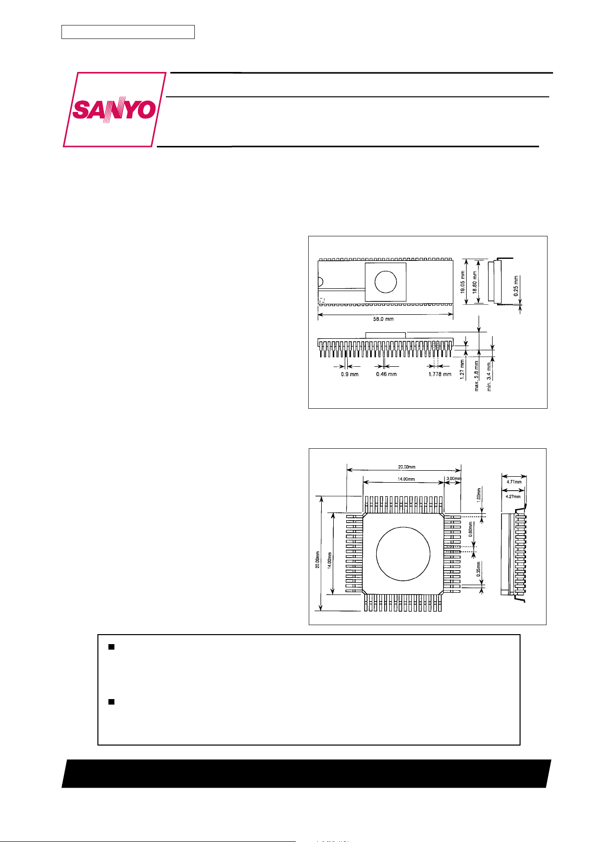
Package Dimensions
unit : mm
3126-DIC64S
[LC86E6032]
SANYO : DIC64S
unit : mm
3152-QFC64E
[LC86E6032]
SANYO : QIC64E
Any and all SANYO products described or contained herein do not have specifications that can handle
applications that require extremely high levels of reliability, such as life-support systems, aircraft’s
control systems, or other applications whose failure can be reasonably expected to result in serious
physical and/or material damage. Consult with your SANYO representative nearest you before using
any SANYO products described or contained herein in such applications.
SANYO assumes no responsibility for equipment failures that result from using products at values that
exceed, even momentarily, rated values (such as maximum ratings, operating condition ranges, or other
parameters) listed in products specifications of any and all SANYO products described or contained
herein.
SANYO Electric Co.,Ltd. Semiconductor Bussiness Headquarters
SANYO Electric Co., Ltd. Semiconductor LSI Div. Microcomputer Development Dep.
TOKYO OFFICE Tokyo Bldg., 1-10, 1 Chome, Ueno, Taito-ku, TOKYO, 110-8534 JAPAN
D3098HA (II)/6232JN
No. 4300-1/19
Page 2
LC86E6032
Notice for Use
LC86E6032 is provided for the program development and checking the function of LC866000A series.
At using, take notice of the followings.
(1) Reset
It is necessary to be sure to go into ‘L’ level and hold for 200 µs to reset terminal (RES) after power supplied voltage has been over
inferior limit of supply voltage.
The option is specified until 3ms after going into ‘H’ level to reset terminal by degrees.
The program is executed from 00H of program counter. The output form of all ports are N-channel open-drain while ‘L’ level to
reset terminal.
(2) Option
The LC86E6032 uses 256 bytes addressed 7F00H to 7FFFH in program memory as option data area.
This area does not affect the execution of program but means that the LC866032A program memory is 32512 bytes addressed
0000H to 7EFFH.
The option data is specified by the option-setting program “SU866000.EXE”. The specified option data is linked to the program
area by linkage editor “L866000.EXE”.
(3) ROM space
7FFFH
7F00H
Option data
Option data
area 256 bytes
area 256 bytes
Option
Option
Data Area
Data Area
Option
Option
Data Area
Data Area
Option
Option
Data Area
Data Area
Option
Option
Data Area
Data Area
7EFFH
6FFFH
5FFFH
4FFFH
3FFFH
2FFFH
1FFFH
Program
Area
Program
Area
Program
Area
Program
Area
Program
Area
32K 28K 24K 20K 16K 12K 8K
0000H
LC866032B LC866028B LC866024B LC866020A LC866016A LC866012A LC866008A
(4) Points of difference LC86E6032 and LC866000A series (mask ROM version)
Item LC86E6032 LC866032B/28B/24B/20A/16A/12A/08A
Operating temperature range +10°C to +40°C–30°C to +70°C
(Topr)
Output form of port at reset Open-drain output Output form specified by option data
Output form of segment Pulldown resistance Pulldown resistance: Provided/ Not provided
S0/T0 to S6/T6 Not provided Specified by option
S7/T7 to S15/T15 Provided (fixed) Provided (fixed)
S16 to S23 Provided (fixed) Specified by option
S24 to S29 Not provided Specified by option
Operating supply 4.5 to 6.0V 2.5 to 6.0V
voltage range (VDD)
Option
Option
Data Area
Data Area
Program
Area
Option
Option
Data Area
Data Area
Program
Area
No. 4300-2/19
Page 3
LC86E6032
Option
A kind of option corresponding LC86E6032
Option types Pins, Circuits Contents of option
Input/output form of Port 0 1.Input:No Pullup MOS Transistor
input/output ports (specified in a bit) Output :N-channel open-drain
Port 1 1.Input :Programmable pullup MOS Transistor
(specified in a bit) Output :N-channel open-drain
Pullup MOS Transistor Port 7 1. No Pullup MOS Transistor
of input port (specified in a bit) 2. Pullup MOS Transistor
2.Input :Pullup MOS Transistor
Output :CMOS
2.Input :Programmable pullup MOS Transistor
Output :CMOS
A kind of option not corresponding LC86E6032
Option types Pins,Circuits Contents of option
Pulldown resistance of S0/T0 to S6/T6 1. Pulldown resistance
high voltage withstand S16 to S29 2. No Pulldown resistance
output terminal (specified in a bit)
How to Use
(1) Specification of options
LC86E6032 must be programmed after specifying option data. The option is specified by “SU866000.EXE”. The specified
option file and the file created by our macro assembler “M866000.EXE” are linked by our linkage loader “L866000.EXE”
which creates .HEX file, then the option code is put in the option specifed area (7F00H to 7FFFH) of its .HEX file.
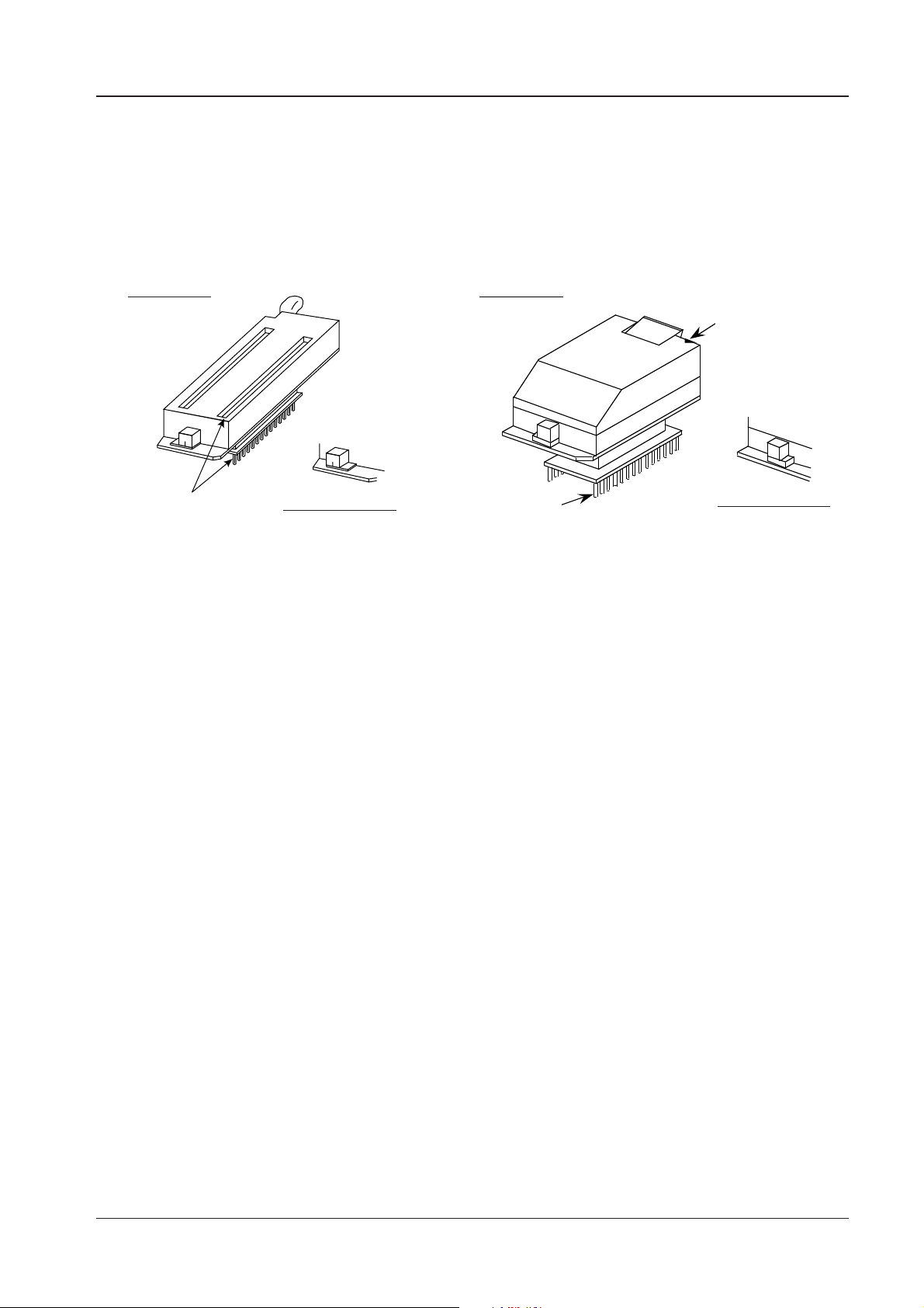
(2) How to write data to EPROM
When writing data that was created by the linker to the LC86E6032, a general-purpose EPROM programmer can be used by
using special write conversion boards (W86EP6032D, W86EP6032Q).
• Recommended EPROM programmers
Supplier EPROM programmer
Advantest R4945, R4944, R4943
Andou AF-9704
AVAL PKW-1100, PKW-3000
Minato Electronics MODEL 1890A
• “27512 (Vp-p = 12.5 V) Intel high-speed programming” mode should be used. The address must be set to "0000H to
7FFFH" and the
jumper (DASEC) must be set 'OFF' at programming.
(3) How to use the data security function
"Data security" is a function to prevent the EPROM data from being read.
Instructions on using the data security function:
1. Set the jumper (DASEC) of the attachment 'ON'.
2. Attempt to program the EPROM.
The EPROM programmer displays an error. The error is a result of normal activity of the data security feature, and
does not indicate a problem with the programmer or the LSI.
Notes
• The data security function is not carried out when the data of all address contain 'FF' at step 2 above.
• Data security cannot be executed when the sequential writing operation of programming
"BLANK=>PROGRAM=>VERIFY" is used at step 2 above.
• Set the jumper 'OFF' after the execution of data security.
No. 4300-3/19
Page 4
LC86E6032
(4) Erasing data
Use a general-purpose EPROM eraser to erase the written data.
(5) Shielding
The UVEPROM (ultraviolet erasable programmable ROM) is incorporated in the IC. Cover the window of the IC with a seal
in use.
Data security
OFF
ON
Pin 1
Data security
OFF
1 pin
Pin 1
ON
OFF
ON
Data security OFF
W86EP6032D W86EP6032Q
1 pin mark
Pin 1 mark
of LSI
OFF
ON
Not data security
Data security OFF
No. 4300-4/19
Page 5
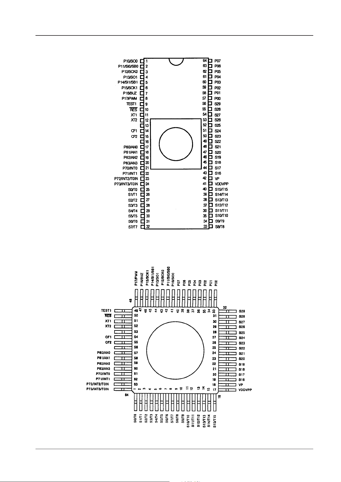
Pin Assignment
LC86E6032
V
SS
V
DD
Pin Assignment
Top view
V
SS
V
DD
Top view
No. 4300-5/19
Page 6
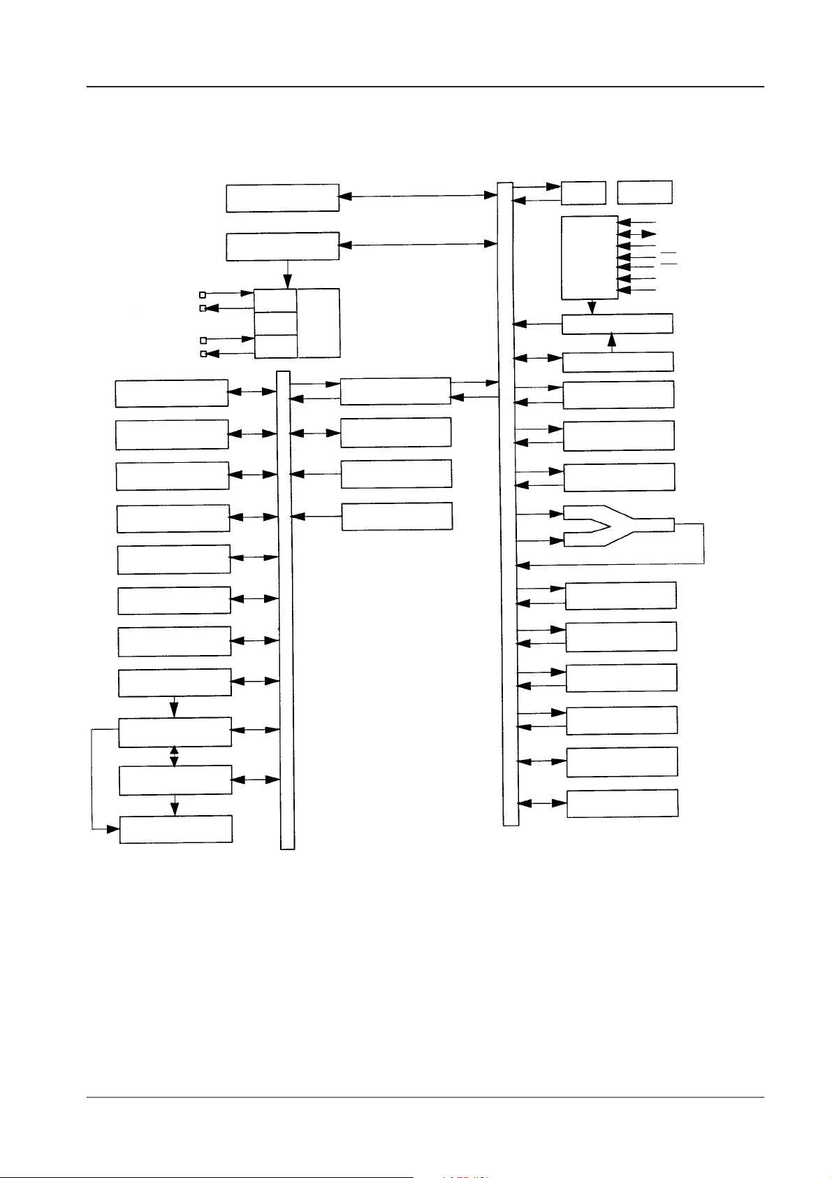
System Block Diagram
LC86E6032
Base timer
SIO0
SIO1
Timer 0
Timer 1
ADC
INT0 to INT3
Noise filter
Interrupt control
Standby control
CF
RC
X'tal
Bus
Clock
generator
Bus interface
Port 1
Port 7
Port 8
Bus
IR PLA
EPROM
control
EPROM(32KB)
PC
ACC
B register
C register
ALU
PSW
RAR
A15 to A0
D7 to D0
TA
CE
OE
DASEC
VDDVPP
Real-time
service
XRAM
(128 bytes)
VFD controller
High voltage
output
RAM
Stack pointer
Port 0
Watchdog timer
No. 4300-6/19
Page 7

LC86E6032
Pin Description
Pin name I/O Function description Option Function in PROM mode
V
SS
V
DD
VP — Power supply pin (–)
VDDVPP — Power supply pin (+) Power for programming
PORT0 I/O • 8-bit input/output port • Pull-up resistor :
P00 to P07 • Input/output specification can be made Provided/Not provided
PORT1 I/O • 8-bit input/output port Output form : CMOS/ Data input/output
P10 to P17 • Data direction can be specified for each bit. N-channel open-drain • D0 to D7
PORT7 • 4-bit input port • Pull-up resistor :
P70 I/O P70 : INT0 input/HOLD release/N-channel Input of PROM control signal
P71 to P73 I P71 : INT 1 input/HOLD release. • DASEC(*1)
— Power supply pin (–)
— Power supply pin (+)
(Power supply for VFD display drive output)
(Power supply for pull-down resistor)
for 4-bit unit. • Output form : CMOS/
• Input for HOLD release N-channel open-drain.
• Input for port 0 interrupt
• Other pin functions
P10 : SIO0 data output
P11 : SIO0 data input/ bus input/output
P12 : SIO0 clock input/output
P13 : SIO1 data output
P14 : SIO1 data input/ bus input/output
P15 : SIO1 clock input/output
P16 : Buzzer output
P17 : Timer 1 output (PWM output)
• Other pin functions Provided/Not provided
transistor output for watchdog timer.
P72 : INT 2 input/timer 0 event input. • OE (*2)
P73 : INT 3 input with noise filter/timer 0 • CE (*3)
event input.
• Interrupt received format, vector address.
Rising Falling Rising High Low Vector
& level level
falling
INT0 Enable Enable Disable Enable Enable 03H
INT1 Enable Enable Disable Enable Enable 0BH
INT2 Enable Enable Enable Disable Disable 13H
INT3 Enable Enable Enable Disable Disable 1BH
PORT8 I • 4-bit input port
P80 to P83 • Other functions
AD input port (4 port pins)
S0/T0 to O Output for VFD display controller
S6/T6 Segment/timing common output
S7/T7 to O Output for VFD display controller •S14/T14 : TA (*4)
S15/T15 Segment/timing common output •S15/T15 : A14 (*5)
Output with built-in pull-down resistor
Continued on next page.
No. 4300-7/19
Page 8

LC86E6032
Continued from preceding page.
Pin name I/O Function description Option Function in PROM mode
S16 to S23 O Output for VFD display controller Address input
Segment output •A13 to A0
Output with built-in pull-down resistor
S24 to S29 O Output for VFD display controller
Segment output
RES I Reset pin
TEST1 O Test pin
Should be left open.
XT1 I Input pin for 32.768 kHz crystal oscillation
When not used, connect to VDD.
XT2 O Output pin for 32.768 kHz crystal oscillation
When not used, should be left open.
CF1 I Input pin for ceramic resonator oscillation
CF2 O Output pin for ceramic resonator oscillation
*1 Memory select input for data security
*2 Output enable input
*3 Chip enable input
*4 TA ➝ PROM control signal input
*5 A14 ➝ Address input
* All of port options can be specified in bit unit.
* A state of pins at reset.
Pin name Input/output mode A state of pullup
Ports 0,7 Input Fixd pullup resistor exsists
Port 1 Input Programmable pullup resistor OFF
Pin name A state of P-channel transistor
S0/T0 to S15/T15 P-channel transistor OFF
S16 to S29 P-channel transistor OFF
resistor
specified at pullup option
No. 4300-8/19
Page 9

LC86E6032
Specification
1. Absolute Maximum Ratings at Ta = 25°C, VSS = 0 V
Parameter Symbol Pins Conditions Ratings Unit
VDD[V] min typ max
Maximum supply VDD max VDD,VDDVPP VDD = VDDVPP –0.3 +7.0 V
voltage
Input voltage VI(1) • P 71, 72, 73 –0.3 VDD+0.3
• Port 8
• RES
VI(2) VP VDD–45 VDD+0.3
Output voltage V
Input/output V
O
IO
voltage
High-
level
output
current
Lowlevel
output
current
Peak
output
current
Total
output
current
Peak
output
current
Total
output
current
∑I
∑I
∑I
∑I
∑I
I
OPH
I
OPH
I
OPH
I
OPL
I
OPL
OAH
OAH
OAH
OAL
OAL
Allowable power Pd max(1) DIC64S Ta = +10°C to +40°C 760 mW
dissipation
Pd max(2) QFC64E Ta = +10°C to +40°C
Operating Topr +10 +40 °C
temperature range
Storage Tstg –65 150
temperature range
• S0/T0 to S15/T15 VDD–45 VDD+0.3
• S16 to S29
Ports 0, 1,P 70 –0.3 VDD+0.3
(1) Ports 0, 1 • CMOS output –4 mA
• At each pin
(2) S0/T0 to S15/T15 At each pin –30
(3) S16 to S29 At each pin –15
(1) Port 0 Total of all pins –10
(2) Port 1 Total of all pins –10
(3) • S0/T0 to S15/T15 Total of all pins –130
• S16 to S29
(1) Ports 0, 1 At each pin 20
(2) P70 At each pin 15
(1) Port 0 Total of all pins –30
(2) Port 1,P70 Total of all pins 40
To be determined after evaluation
No. 4300-9/19
Page 10

LC86E6032
2. Allowable Operating Conditions at Ta = +10°C to +40°C, VSS = 0 V
Parameter Symbol Pins Conditions Ratings Unit
VDD[V] min typ max
Operating supply V
DD
voltage range tCYC ≤ 400 µs
HOLD voltage V
HD
Pulldown supply VP VP 4.5 to 6.0 –35 V
voltage
Input high-level VIH(1) Port 0 (Schmitt) Output disable 4.5 to 6.0 0.4V
voltage +0.9
VIH(2) • Port 1 Output disable 4.5 to 6.0 0.75V
VIH(3) • P70 Output N-channel 4.5 to 6.0 0.75V
VIH(4) P70 Output N-channel 4.5 to 6.0 0.9V
VIH(5) • Port 8 4.5 to 6.0 0.75V
Input low-level VIL(1) Port 0 (Schmitt) Output disable 4.5 to 6.0 V
voltage
VIL(2) • Port 1 Output disable 4.5 to 6.0 V
VIL(3) •P70 N-channel transistor 4.5 to 6.0 V
VIL(4) P70 N-channel transistor 4.5 to 6.0 V
VIL(5) •Port 8 4.5 to 6.0 V
Operation cycle tCYC 4.5 to 6.0 0.98 400 µs
time
Oscillation FmCF(1) CF1, CF2 •12 MHz (ceramic 4.5 to 6.0 11.76 12 12.24 MHz
frequency range resonator oscillation).
(Note 1) •Refer to Figure 1.
FmCF(2) CF1, CF2 •3 MHz (ceramic 4.5 to 6.0 2.94 3 3.06
FmRC RC oscillation 4.5 to 6.0 0.4 0.8 2.0
FsXtal XT1, XT2 • 32.768 kHz (crystal 4.5 to 6.0 32.768 kHz
Oscillation stable tmsCF(1) CF1, CF2 •12 MHz (ceramic 4.5 to 6.0 0.02 0.2 ms
time period resonator oscillation).
(Note 1) •Refer to Figure 3.
tmsCF(2) CF1, CF2 • 3 MHz (ceramic 4.5 to 6.0 0.1 1
tssXtal XT1, XT2 •32.768 kHz (crystal 4.5 to 6.0 1 1.5 s
(Note 1) Refer to Table 1 and Table 2 for the oscillation constants.
V
DD
V
DD
0.98 µs ≤ tCYC 4.5 6.0 V
• When in HOLD mode 2.0 6.0
• RAM and registers
retain previous data.
DD
DD
DD
V
DD
V
DD
• P72, 73
(Schmitt)
DD
V
DD
Port input/interrupt. transistor OFF
• P71
• RES (Schmitt)
DD
V
DD
Watchdog timer transistor OFF
DD
SS
SS
V
0.2V
0.25V
DD
DD
• P72, 73(Schmitt)
SS
0.25V
Port input/interrupt. OFF
•P71
•RES (Schmitt)
SS
0.8V
DD
Watchdog timer OFF –1.0
SS
0.25V
resonator oscillation).
•Refer to Figure 1.
oscillation).
•Refer to Figure 2.
resonator oscillation).
•Refer to Figure 3.
oscillation).
•Refer to Figure 3.
DD
DD
DD
No. 4300-10/19
Page 11

LC86E6032
3. Electrical Characteristics at Ta= +10°C to +40°C , VSS = 0 V
Parameter Symbol Pins Conditions Ratings Unit
VDD [V] min typ max
Input high-level
current
Input low-level
current
Output high-level
voltage
Output low-level
voltage
IIH(1) 4.5 to 6.0 1 µA
•Port 1
•Port 0 without
pull-up MOS
transistor
•Output disable
•Pull-up MOS transistor
OFF.
•VIN = V
DD
(including off-state leak
current of output
transistor)
IIH(2) 4.5 to 6.0 1
•Port 7 without
VIN= V
DD
pull-up MOS
transistor
•Port 8
IIH(3) 4.5 to 6.0 1
IIL(1) 4.5 to 6.0 –1
•RES
•Port 1
•Port 0 without
pull-up MOS
transistor
VIN = V
DD
•Output disable
•Pull-up MOS transistor
OFF.
•VIN = V
SS
(including off-state leak
current of output
transistor)
IIL(2) 4.5 to 6.0 –1
•Port 7
VIN = V
SS
without pull-up
MOS transistor
•Port 8
IIL(3) 4.5 to 6.0 –1
VOH(1) 4.5 to 6.0 VDD–1 V
VOH(2) 4.5 to 6.0 VDD–0.5
VOH(3) 4.5 to 6.0 VDD–1.8
•RES
•Ports 0, 1 at CMOS
output
S0/T0 to S15/T15
VOH(4) 4.5 to 6.0 VDD–1
VIN = V
SS
IOH = –1.0 mA
IOH = –0.1 mA
IOH = –20 mA
•IOH= –1.0 mA
•The current of any
unmeasurement pin is
not over 1 mA.
VOH(5) 4.5 to 6.0 VDD–1.8
S16 to S29
VOH(6) 4.5 to 6.0 VDD–1
IOH = –5 mA
•IOH= –1.0 mA
•The current of any
unmeasurement pin is
not over 1 mA.
VOL(1) 4.5 to 6.0 1.5
Ports 0,1
VOL(2) 4.5 to 6.0 0.4
IOL = 10 mA
•IOL = 1.6 mA
•The total current of the
Ports 0,1 is not over
40 mA
Pull-up MOS
transistor resistor
Output off-state
leak current
VOL(3) 4.5 to 6.0 0.4
Rpu 4.5 to 6.0 15 40 70 kΩ
P70
•Ports 0, 1
IOL = 1 mA
VOH = 0.9 V
DD
•Port 7
I
OFF
•S0/T0 to S6/T6
(1) 4.5 to 6.0 –1 µA
•S24 to S29
(Without pulldown
I
OFF
resistor)
(2) 4.5 to 6.0 –30
•Output P-channel
transistor OFF.
•V
= Vss
OUT
•Output P-channel
transistor OFF.
•V
= VDD–40V
OUT
Continued on next page.
No. 4300-11/19
Page 12

LC86E6032
Continued from preceding page.
Parameter Symbol Pins Conditions Ratings Unit
VDD [V] min typ max
Pulldown resistor
Hysteresis
voltage
R
V
pd
HIS
• S7/T7 to S15T15
• S16 to S23
(With pulldown
resistor)
•Ports 0,1
•Port 7
•RES
•Output P-channel
transistor OFF.
•V
= 3V
OUT
•VP= –30V
•Output disable
5.0 60 100 200 kΩ
4.5 to 6.0 0.1V
DD
V
Pin capacitance
CP 4.5 to 6.0 10 pF
All pins
•f=1MHz
•Unmeasurement
terminals for input
are set to VSS level.
•Ta= 25°C
4. Serial Input/Output Characteristics at Ta = +10°C to +40°C , VSS = 0 V
Parameter Symbol Pins Conditions Ratings Unit
VDD [V] min typ max
Cycle
Low-
level
pulse
width
Input clock
Highlevel
pulse
width
Cycle
Serial clock
Lowlevel
pulse
width
Output clock
Highlevel
pulse
width
Data set-up
time
Data hold
time
Serial input
Output delay
time
(Serial clock
is extrnal
clock.)
Output delay
Serial output
time
(Serial clock
is internal
clock.)
tCKCY(1) SCK0, SCK1 4.5 to 6.0 2 tCYC
tCKL(1) 4.5 to 6.0 1
tCKH(1) 4.5 to 6.0 1
tCKCY(2) SCK0, SCK1 4.5 to 6.0 2
tCKL(2) 4.5 to 6.0 1/2tCKCY
tCKH(2) 4.5 to 6.0 1/2tCKCY
tICK • SI0, SI1 4.5 to 6.0 0.1 µs
• SB0, SB1
tCKI
tCKO(1) • SO0, SO1
• SB0, SB1 +0.2
tCKO(2)
• SO0, SO1
• SB0, SB1 +0.2
Refer to Figure 5.
•Use pull-up resistor
(1 kΩ) when set to
open-drain output.
•Refer to Figure 5.
•Data set-up to
SCK0, 1
•Refer to Figure 5.
•Data hold from
SCK0, 1
•Use pull-up resistor
(1 kΩ) when set to
open-drain output.
•Refer to Figure 5.
•Data hold from
SCK0, 1
•Use pull-up resistor
(1 kΩ) when set to
open-drain output.
•Refer to Figure 5.
4.5 to 6.0 0.1
4.5 to 6.0 7/12tCYC
4.5 to 6.0 1/3tCYC
No. 4300-12/19
Page 13

LC86E6032
5. Pulse Input Conditions at Ta = +10°C to +40°C, VSS = 0 V
Parameter Symbol Pins Conditions Ratings Unit
VDD [V] min typ max
High/low-level tPIH(1) • INT0, INT1 4.5 to 6.0 1 tCYC
pulse width tPIL(1) • INT2/T0IN
tPIH(2) INT3/T0IN 4.5 to 6.0 2
tPIL(2) (The noise rejection
clock selected to 1/1.)
tPIH(3) INT3/T0IN 4.5 to 6.0 128
tPIL(3) (The noise rejection
clock selected to 1/64.)
tPIL(4) RES 4.5 to 6.0 200 µs
6. A/D Converter Characteristics at Ta = +10°C to +40°C, VSS = 0 V
Parameter Symbol Pins Conditions Ratings Unit
Resolution
Absolute precision
Conversion time
Analog input
voltage range
Analog port
input current
N 4.5 to 6.0 8 bit
ET ±1.5 LSB
tCAD 15.68 65.28 µs
V
I
AINH
I
AINL
AIN
AN0 to AN3 V
• Interrupt acceptable
• Timer 0 pulse
countable
• Interrupt acceptable
• Timer 0 pulse
countable
• Interrupt acceptable
• Timer 0 pulse
countable
Reset acceptable
(Note 2)
A/D conversion time
= 16 x tCYC
(ADCR2 = 0)
(Note 3)
A/D conversion time
= 32 x tCYC
(ADCR2 = 1)
(Note 3)
V
= V
AIN
DD
V
= V
AIN
SS
VDD [V] min typ max
(tCYC = (tCYC =
0.98 µs) 4.08 µs)
31.36 130.56
(tCYC = (tCYC =
0.98 µs) 4.08 µs)
SS
V
–1
DD
1 µA
V
(Note 2) Absolute precision excepts quantizing error (±1/2 LSB).
(Note 3) The conversion time is the time from execution of the instruction to start conversion to the completion of shifting the
A/D converted value to the register.
No. 4300-13/19
Page 14

LC86E6032
7. Current Drain Characteristics at Ta = +10°C to +40°C , VSS = 0 V
Parameter Symbol Pins Conditions Ratings Unit
VDD [V] min typ max
Current drain
during basic
operation
(Note 4)
I
(1) V
DDOP
I
(2) 4.5 to 6.0 6.5 14
DDOP
I
(3) 4.5 to 6.0 4 10
DDOP
I
(4) 4.5 to 6.0 3.5 9
DDOP
DD
•FmCF = 12 MHz for
ceramic resonator
oscillation.
•FsXtal = 32.768 kHz for
crystal oscillator.
•System clock :
12 MHz side
•Internal RC oscillator
stopped.
•FmCF = 3 MHz for
ceramic resonator
oscillation.
•FsXtal = 32.768 kHz for
crystal oscillator.
•System clock :
3 MHz side
•Internal RC oscillator
stopped.
•FmCF = 0 Hz
(when oscillator stops).
•FsXtal = 32.768 kHz for
crystal oscillator.
•System clock :
RC oscillator.
•FmCF = 0 Hz
(when oscillator stops).
•FsXtal = 32.768 kHz for
crystal oscillator.
•System clock :
32.768 kHz side
•Internal RC oscillator
stopped.
4.5 to 6.0 13 26 mA
Continued on next page.
No. 4300-14/19
Page 15

LC86E6032
Continued from preceding page.
Parameter Symbol Pins Conditions Ratings Unit
VDD [V] min typ max
I
Current drain at
HALT mode
(Note 4)
Current drain at
HOLD mode
(Note 4)
(1) V
DDHALT
DD
•HALT mode
•FmCF = 12 MHz for
ceramic resonator
oscillation.
•FsXtal = 32.768 kHz for
crystal oscillator.
•System clock :
12 MHz side
•Internal RC oscillator
stopped.
I
(2) 4.5 to 6.0 1.8 4.6
DDHALT
•HALT mode
•FmCF = 3 MHz for
ceramic resonator
oscillation.
•FsXtal = 32.768 kHz for
crystal oscillator.
•System clock :
3 MHz side
•Internal RC oscillator
stopped.
I
(3) 4.5 to 6.0 400 800 µA
DDHALT
•HALT mode
•FmCF = 0 Hz
(when oscillator stops).
•FsXtal = 32.768 kHz for
crystal oscillator.
•System clock :
RC oscillator
I
(4) 4.5 to 6.0 20 60
DDHALT
•HALT mode
•FmCF = 0 Hz
(when oscillator stops).
•FsXtal = 32.768 kHz for
crystal oscillator.
•System clock :
32.768 kHz side
•Internal RC oscillator
stopped.
I
(1) V
DDHOLD
I
(2) 2.5 to 4.5 0.02 20
DDHOLD
DD
HOLD mode
4.5 to 6.0 5 10 mA
4.5 to 6.0 0.05 30
(Note 4) The currents of output transistors and pull-up MOS transistors are ignored.
No. 4300-15/19
Page 16

LC86E6032
Oscillation type Supplier Oscillator C1 C2
12 MHz ceramic resonator Murata CSA12.0MTZ 33 pF 33 pF
oscillation CSA12.0MT 33 pF 33 pF
CST12.0MTW on chip
Kyocera KBR–12.0M 33 pF 33 pF
3 MHz ceramic resonator Murata CSA3.00MG 33pF 33 pF
oscillation CST3.00MGW on chip
Kyocera KBR–3.0MS 47 pF 47 pF
* Both C1 and C2 must use K rank (±10%) and SL characteristics.
Table 1. Ceramic Resonator Oscillation Guaranteed Constants (Main-clock)
Oscillation type Supplier Oscillator C3 C4
32.768 kHz crystal oscillation Dai Sinku DT-38(1TA252E00) 18 pF 18 pF
Kyocera KF-38G-13P0200 18 pF 18 pF
* Both C3 and C4 must use J rank (±5%) and CH characteristics.
(If high precision is unnecessary, use K rank (±10%) and SL characteristics.)
Table 2. Crystal Oscillation Guaranteed Constants (Sub-clock)
Notes • Since the circuit pattern affects the oscillation frequency, place the oscillation-related parts as close to the oscillation pins
as possible with the shortest pattern length.
• If you use other oscillators herein, we provide no guarantee for the characteristics.
CF1
CF X'talC1
Main-clock circuit Sub-clock circuit
Figure 1 Ceramic Resonator Oscillation Figure 2 Crystal Oscillation
CF2
C2
XT1
C3 C4
XT2
No. 4300-16/19
Page 17

LC86E6032
V
DD
VDD
VDD lower limit
Power supply
Reset time
RES
Internal RC
resonator
oscillation
t
msCF
CF1, CF2
t
ssXtal
XT1,XT2
Operation mode Unfixed Reset Instruction execution mode
< Reset time and oscillation stable time. >
VDD
0V
limit
HOLD release signal
Valid
Internal RC
resonator
oscillation
t
msCF
CF1, CF2
t
ssXtal
XT1,XT2
Operation mode Instruction execution mode
HOLD
< HOLD release signal and oscillation stable time. >
Figure 3 Oscillation Stable Time
VDD
V
DD
RRES
RES
(Note)
(Note) Fix the value of C
CRES
The values of C
is sure to reset untill 200µs, after
reset time is at least 200 µs, measured from the moment the
power exceeds the V
Power supply has been over inferior
limit of supply voltage.
Figure 4 Reset Circuit
RES
and R
RES
should be determined such that
RES
lower limit.
DD
, R
RES
that
No. 4300-17/19
Page 18

LC86E6032
0.5VDD
0.5V
DD
< AC timing point >
< AC timing point >
tCKCY
tCKL tCKH
V
VDD
DD
SCK0
SCK1
SI0
SI1
SO0,SO1
SB0,SB1
tCKItICK
tCKO
< Timing >
Figure 5 Serial Input/Output Test Conditions
1kΩ
50pF
< Test load >
t
PIL
Figure 6 Pulse Input Timing Conditions
t
PIH
No. 4300-18/19
Page 19

LC86E6032
Specifications of any and all SANYO products described or contained herein stipulate the performance,
characteristics, and functions of the described products in the independent state, and are not guarantees
of the performance, characteristics, and functions of the described products as mounted in the customer’s
products or equipment. To verify symptoms and states that cannot be evaluated in an independent device,
the customer should always evaluate and test devices mounted in the customer’s products or equipment.
SANYO Electric Co., Ltd. strives to supply high-quality high-reliability products. However, any and all
semiconductor products fail with some probability. It is possible that these probabilistic failures could
give rise to accidents or events that could endanger human lives, that could give rise to smoke or fire,
or that could cause damage to other property. When designing equipment, adopt safety measures so
that these kinds of accidents or events cannot occur. Such measures include but are not limited to protective
circuits and error prevention circuits for safe design, redundant design, and structural design.
In the event that any or all SANYO products(including technical data,services) described or
contained herein are controlled under any of applicable local export control laws and regulations,
such products must not be exported without obtaining the export license from the authorities
concerned in accordance with the above law.
No part of this publication may be reproduced or transmitted in any form or by any means, electronic or
mechanical, including photocopying and recording, or any information storage or retrieval system,
or otherwise, without the prior written permission of SANYO Electric Co. , Ltd.
Any and all information described or contained herein are subject to change without notice due to
product/technology improvement, etc. When designing equipment, refer to the “Delivery Specification”
for the SANYO product that you intend to use.
Information (including circuit diagrams and circuit parameters) herein is for example only ; it is not
guaranteed for volume production. SANYO believes information herein is accurate and reliable, but
no guarantees are made or implied regarding its use or any infringements of intellectual property rights
or other rights of third parties.
This catalog provides information as of December, 1998. Specifications and information herein are subject to
change without notice.
No. 4300-19/19
PS
 Loading...