

Page 1

Ordering number : ENN*6710
LC868901/51
LC868901/51
Row Driver IC for Dot Matrix Graphic LCD
Preliminary
Overview
The LC868901 sereis is a common driver for the liquid crystal dot-matrix graphic display. It generates 65 commons
maximum. The LC868901series has the RC-oscillator circuit attached resistor and the capacitor outside, and
generates the timing signals and LCD powers for the LC868900 segmentdrivers.
As the LC868901 series is fabricated using CMOS process technology, combining it with a CMOS microcontroller
produces an LCD device of low power demand.
Features
• Classification
Interfacing allowed for 80-family and our LC868000 microcontroller :LC868901
Interfacing allowed for Motorola family :LC868951
• 65 common outputs
• Automatic LCD display controller
Duty 1 / 1 to 1 / 65 (programmable)
Bias 1 / 5, 1 / 7 and 1 / 9 (programmable)
Contrasts 32-step programmable
Instructions
Display on / off
Horizontal display bit control
[Horizontal display number] ✕ [Display pitch (bit length)]
Busy flag readable
• Built-in power booster
• Stand-by function
Two kinds of stand-by setting
1. Applying low level to STB
2. Programming
Stand-by releasing
Read after applying low level to CS and RD
• Oscillator
RC oscillator must be attached resistor and the capacitor outside.
• Power supply
Logic circuit 3V to 5V (VDD)
• CMOS process
• Factory shipment
Chip delivery form
QFP100E package
CMOS IC
Ver. 1.01
61295
Any and all SANYO products described or contained herein do not have specifications that can handle
applications that require extremely high levels of reliability, such as life-support systems, aircraft's
control systems, or other applications whose failure can be reasonably expected to result in serious
physical and/or material damage. Consult with your SANYO representative nearest you before using
any SANYO products described or contained herein in such applications.
SANYO assumes no responsibility for equipment failures that result from using products at values that
exceed, even momentarily, rated values (such as maximum ratings, operating condition ranges, or other
parameters) listed in products specifications of any and all SANYO products described or contained
herein.
SANYO Electric Co.,Ltd. Semiconductor Company
TOKYO OFFICE Tokyo Bldg., 1-10, 1 Chome, Ueno, Taito-ku, TOKYO, 110-8534 JAPAN
D2800 RM (IM) FS
No.6710-1/20
Page 2
Pin Assignment
XV5
XV4
XV3
XV2
XV1
RES
V
DD
OSC1
OSC2
V
SS
DB0
DB1
DB2
DB3
DB4
DB5
DB6
DB7
(NC)
(NC)
100
80
81
82
83
84
85
86
87
88
89
90
91
92
93
94
95
96
97
98
99
V3
1
1
V
(NC)
79
78
3
2
EE
2
EE
V
77
4
VOT1
76
5
VOT2
75
6
CAP2
CAP1
74
8
7
LC868901/51
C3
C4
C2
C1
727173
13
12
11
10
9
C5
687069
C6
67
14
C7
66
15
C8
65
16
C10
C11
C12
C13
C14
C15
C16
C9
6261605958575655545352
64
63
22
212023242526272829
19
18
17
C17
C18
C19
C20
C21
49
48
47
46
45
44
43
42
41
40
39
38
37
36
35
34
33
32
31
C22
51
50
C23
C24
C25
C26
C27
C28
C29
C30
C31
C32
C33
C34
C35
C36
C37
C38
C39
C40
C41
C42
30
CS
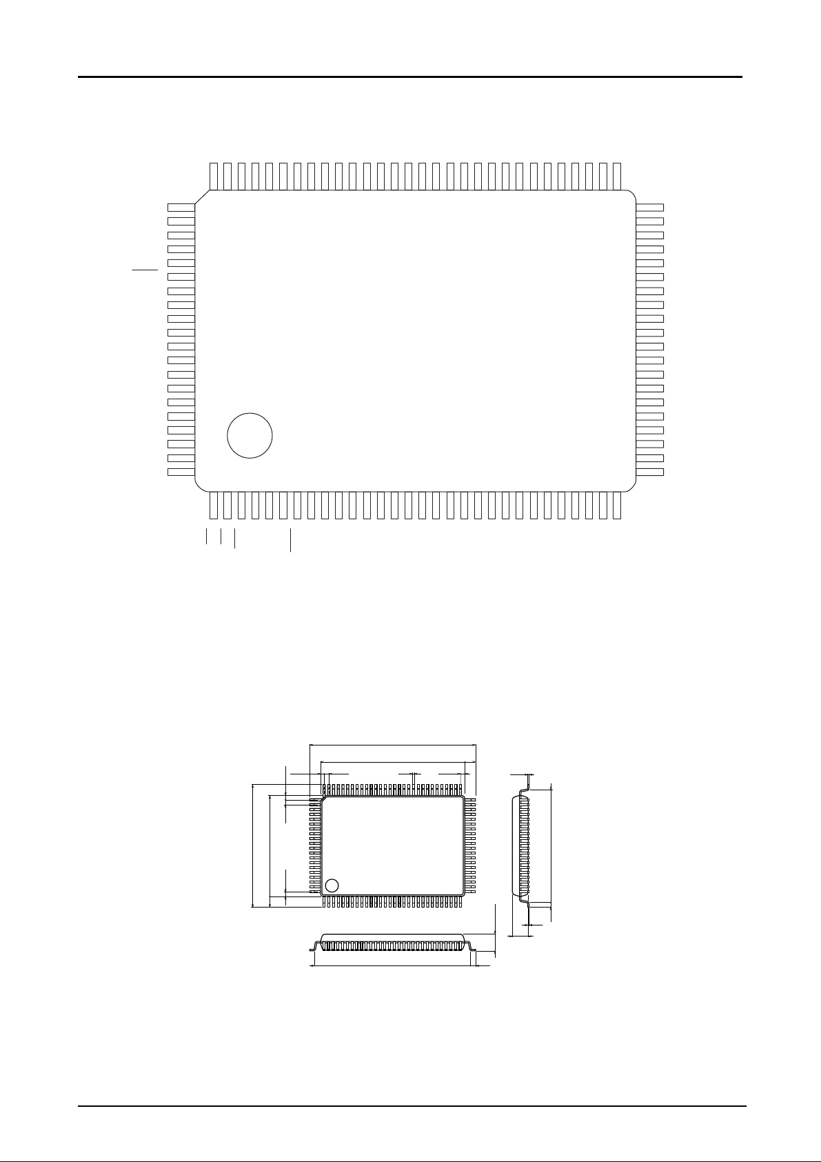
Package Dimension
(unit : mm)
3151
RD
WR
17.2
RS
CL2
14.0
1.6
M
C54
C53
C52
C51
C50
C59
0.3
C56
1.6
0.575
51
50
31
3.0max
C61
C60
C62
C63
C64
C65
STB
23.2
0.575
0.825
0.65
0.825
0.65
80
81
100
130
20.0
C55
C58
C57
C49
0.15
0.1
2.7
C48
15.6
0.8
C47
C46
C45
C44
SANYO : QIP-100E
C43
ILC00202
21.6
0.8
SANYO : QIP-100E
(FLP100)
No.6710-2/20
Page 3

Pads
LC868901/51
Pin No. Pad No.
1 1 CS - - 2113 - - 1645 51 51 C22 2478 1764
2 2 RD - - 1950 - - 1645 52 52 C21 2315 1764
3 3 WR - - 1788 - - 1645 53 53 C20 2153 1764
4 4 RS - - 1625 - - 1645 54 54 C19 1990 1764
5 5 CL2 - - 1463 - - 1645 55 55 C18 1828 1764
6 6 M - - 1300 - - 1645 56 56 C17 1665 1764
7 7 STB - - 1138 - - 1645 57 57 C16 1503 1764
8 8 C65 - - 914 - - 1794 58 58 C15 1340 1764
9 9 C64 - - 752 - - 1794 59 59 C14 1178 1764
10 10 C63 -- 589 - - 1794 60 60 C13 1015 1764
11 11 C62 -- 427 -1794 61 61 C12 853 1764
12 12 C61 -- 264 - - 1794 62 62 C11 690 1764
13 13 C60 -- 102 - - 1794 63 63 C10 528 1764
14 14 C59 61 - - 1794 64 64 C9 365 1764
15 15 C58 223 - - 1794 65 65 C8 203 1764
16 16 C57 386 - - 1794 66 66 C7 40 1764
17 17 C56 548 - - 1794 67 67 C6 - - 122 1764
18 18 C55 711 - - 1794 68 68 C5 - - 285 1764
19 19 C54 873 -1794 69 69 C4 - - 447 1764
20 20 C53 1036 - - 1794 70 70 C3 - - 610 1764
21 21 C52 1198 - - 1794 71 71 C2 - - 772 1764
22 22 C51 1361 - - 1794 72 72 C1 - - 935 1764
23 23 C50 1523 -- 1794 73 73 CAP2 -- 1569 1617
24 24 C49 1686 -- 1794 74 74 CAP1 -- 1732 1617
25 25 C48 1848 -- 1794 75 75 VOT2 -- 1894 1617
26 26 C47 2011 -- 1794 76 76 VOT1 -- 2057 1617
27 27 C46 2173 - - 1794 77 77 VEE2 - - 2278 1617
28 28 C45 2336 - - 1794 78 78 VEE1 - - 2441 1617
29 29 C44 2498 - - 1794 79 - - NC
30 30 C43 2661 -- 1794 80 79 V3 -- 2603 1617
31 31 C42 2690 -- 1482 81 80 XV5 -- 2526 1156
32 32 C41 2690 -- 1320 82 81 XV4 -- 2526 993
33 33 C40 2690 -- 1157 83 82 XV3 -- 2526 831
34 34 C39 2690 -- 995 84 83 XV2 -- 2526 668
35 35 C38 2690 -- 832 85 84 XV1 -- 2526 506
36 36 C37 2690 -- 670 86 85 RES -- 2556 316
37 37 C36 2690 - - 507 87 86 V
38 38 C35 2690 -- 345 88 87 OSC1 -- 2556 -- 9
39 39 C34 2690 -- 182 89 88 OSC2 -- 2556 -- 172
40 40 C33 2690 - - 20 90 89 V
41 41 C32 2690 143 91 90 DB0 - - 2556 - - 497
42 42 C31 2690 305 92 91 DB1 - - 2556 - - 659
43 43 C30 2690 468 93 92 DB2 - - 2556 - - 822
44 44 C29 2690 630 94 93 DB3 - - 2556 - - 984
45 45 C28 2690 793 95 94 DB4 -- 2556 -- 1147
46 46 C27 2690 955 96 95 DB5 -- 2556 -- 1309
47 47 C26 2690 1118 97 96 DB6 -- 2556 -- 1472
48 48 C25 2690 1280 98 97 DB7 -- 2556 -- 1634
49 49 C24 2690 1443 99 -- NC
50 50 C23 2690 1605 100 -- NC
Pad axis
name
X µmYµmX µmYµm
Pin No. Pad No.
Pad axis
name
DD
SS
- - 2556 153
- - 2556 - - 334
Notes 1. Using for chip, the substrate must be shortened to VDD, or left open.
2. Ask the solder-soaking condition for QFP100E package.
No.6710-3/20
Page 4

LC868901/51
Pin function
Pin name Pin No. I / O Description Pin form type
V
SS
V
DD
VEE1, 2 78, 77 -- LCD power pins
VOT1, 2 76, 75 -- Power booster pins
CAP1, 2 74, 73 -- Capacitor connecting pins for power booster
DB0 91 I / O Data bus DB0-4, 7 : C
to DB5, 6 : D
DB7 98
RES 86 Input Reset (active low) B
CS 1 Input Chip select (active low) A
RD 2 Input Read (active low) A
WR 3 Input Write (active low) A
RS 4 Input Register select A
CL2 5 Output LCD clock for data shifting E
M 6 Output LCD clock for synchronizing E
STB 7 Input Stand-by (active low) B
V3 80 Output Monitor pin for LCD power
XV1 to XV5 85 to 81 Output LCD power suppliers
C1 to C65 72 to 8 Output Common outputs for LCD display F
90 -- Negative power pin (-- )
87 -- Positive power pin (+)
RS=1 : instruction register
RS=0 : data register
Block Diagram
OSC1
OSC2
STB
RS
CS
RD
WR
RES
CL2
V
DD
V
SS
C1
LCD DRIVERS
OSCILLATOR
TIMING GENERATOR
M
MODE REGISTER
SYSTEM CLOCK 1
SYSTEM CLOCK 2
C65
POWER
BOOSTER
LCD POWER
CIRCUIT
CONTRAST CONTROL
CIRCUIT
CONTRAST CONTROL
REGISTER
VOT1
VOT2
CAP1
CAP2
V3
XV1
XV2
XV3
XV4
XV5
VEE1
VEE2
DB0
DB1
DB2
DB3
DB4
DB5
DB6
DB7
DATA REGISTER
INSTRUCTION REGISTER
BUSY FLAG
TIME DIVISION
REGISTER
DISPLAY NUMBER
REGISTER
DISPLAY PITCH
REGISTER
MODE REGISTER
ILC00203
No.6710-4/20
Page 5
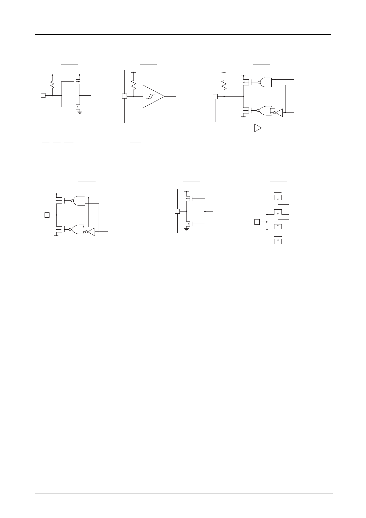
Pin forms
A type B type C type
LC868901/51
V
V
DD
IN
V
SS
ILC00204
IN
DD
IN / OUT
ILC00205
V
DD
V
SS
CS, RD, WR, RS pins RES, STB pins DB0 to DB4, DB7
D type E type F type
V
DD
OUT
V
SS
OUT
V
DD
V
SS
DATA
OUT
OUTPUT CONTROL
DATA
OUTPUT CONTROL
ILC00206
V
DD
V1
V4
V5
ILC00207
ILC00208
ILC00209
DB5, DB6 CL2, M C1 to C65
No.6710-5/20
Page 6
LC868901/51
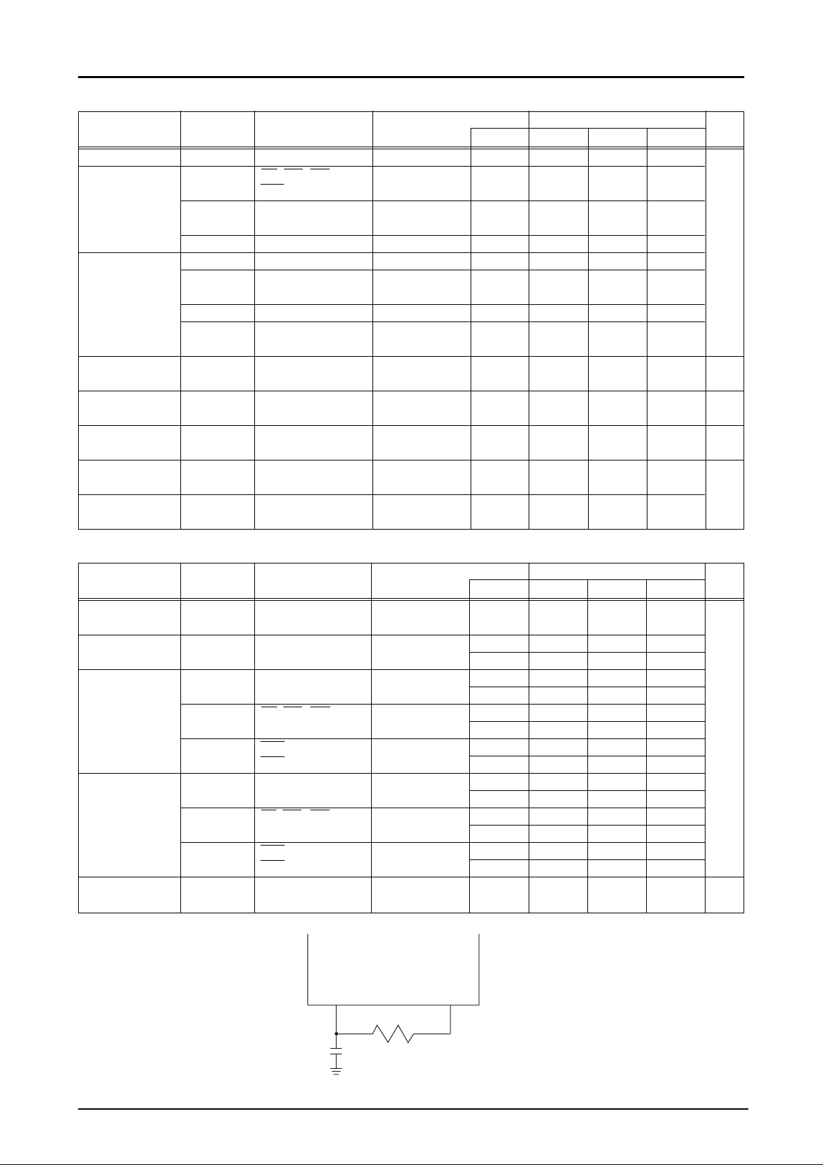
1. Absolute Maximum Ratings at Ta=25°C, VSS=0V
Parameter Symbol Pins Conditions
Supply voltage VDD MAX V
DD
VDD[v] min. typ. max.
-- 0.3 +7.0 V
Input voltage VI(1) CS, RD, WR, RS, -- 0.3 VDD+0.3
RES
VI(2) DB0 to DB7 At input mode -- 0.3 VDD+0.3
Ratings
unit
VI(3) VEE1, VEE2V
Output voltage VO(1) C1 to C65
-- 21 VDD+0.3
DD
VEE2-- 0.3
VDD+0.3
VO(2) DB0 to DB7 At output mode -- 0.3 VDD+0.3
VO(3) M, CL2 -- 0.3 VDD+0.3
VO(4) VOT1, VOT2, VDD-- 21 VDD+0.3
CAP1, CAP2
High-level output
∑IOAH C1 to C65
The total all pins
-- 25 mA
current
Low-level output ∑IOAL C1 to C65
The total all pins
30 mA
current
Maximum power Pdmax QFP100E
Ta= -- 30 to + 70°C
200 mW
dissipation
Operating Topg -- 30 70 °C
temperature limits
Storage Tstg -- 55 150
temperature limits
2. Recommended Operating Limits at Ta= -- 30°C to +70°C, VSS=0V
Parameter Symbol Pins Conditions
Operating supply V
voltage
limits
LCD power supply
voltage
limits
Input high voltage
DD
V
EE
VIH(1) DB0 to DB7 At input mode 4.5 to 6.0 2.2 V
V
DD
VEE1, VEE2 4.5 to 6.0 -- 2V
Ratings
VDD [V] min. typ. max.
2.5 6.0 V
V
DD
V
DD
2.5 to 4.5 -- V
DD
DD
DD
2.5 to 4.5 0.75V
DD
V
DD
unit
VIH(2) CS, RD, WR, RS 4.5 to 6.0 2.2 VDD
2.5 to 4.5 0.75V
DD
V
DD
VIH(3) RES (schmitt), 4.5 to 6.0 0.75VDD VDD
STB (schmitt) 2.5 to 4.5 0.75V
DD
V
DD
Input low voltage VIL(1) DB0 to DB7 At input mode 4.5 to 6.0 0 0.8
VIL(2)
CS, RD, WR, RS
2.5 to 4.5
0
4.5 to 6.0 0 0.8
2.5 to 4.5 0 0.25V
0.25V
DD
DD
VIL(3) RES (schmitt), 4.5 to 6.0 0 0.25VDD
STB (schmitt) 2.5 to 4.5 0 0.25V
DD
Oscillation FRC OSC1, OSC2 •RC oscillation 2.5 to 6.0 20 500 kHz
frequency limits •Fig. 1
OSC1 OSC2
Rext
Cext
Fig.1 RC-oscillator circuit
ILC00210
No.6710-6/20
Page 7

LC868901/51
3. Electrical Characteristics at Ta= -- 30°C to +70°C
Parameter Symbol Pins Conditions
Output high VOH(1) DB80 to DB7 •output mode 4.5 to 6.0
voltage •IOH= -- 1mA
•output mode 2.5 to 6.0
•IOH= -- 0.1mA
VOH(2) M, CL2 IOH= -- 0.4mA 4.5 to 6.0
IOH= -- 0.1mA 2.5 to 6.0
Output low VOL(1) DB0 to DB7 •output mode 4.5 to 6.0 0.4
voltage •IOL=+0.6mA
•output mode 2.5 to 6.0 0.4
•IOH=+0.1mA
VOL(2) M, CL2 IOL=+0.4mA 4.5 to 6.0
IOL=+0.1mA 2.5 to 6.0
Pull-up RPU(1) DB0 to DB7 •input mode 4.5 to 6.0 150 500 900 kΩ
resistance •VIN=0V
•input mode 2.5 to 4.5 300 750 1500
•VIN=0V
RPU(2) CS, RD, WR, RS, VIN=0V 4.5 to 6.0 150 500 900
RES, STB VIN=0V 2.5 to 4.5 300 750 1500
Drop voltage VD(1) C1 to C65 •-- 100µA at each 4.5 to 6.0 150 mV
between Ci pin
VDD and Ci •
(i : 1 to 65) •-- 15µA at each 2.5 to 6.0 120
Drop voltage VD(2) C1 to C65 •-- 100µA at each 4.5 to 6.0 150 mV
between Ci pin
VX and Ci •
(X : 1, 4) •-- 15µA at each 2.5 to 6.0 120
(i : 1 to 65) Ci pin
Drop voltage VD(3) C1 to C65 •+100µA at each 4.5 to 6.0 -- 150 mV
between Ci pin
VX and Ci •
(X : 1, 4) •+15µA at each 2.5 to 6.0 -- 120
(i : 1 to 65) Ci pin
Boosted voltage VOT1 •VOT1 Load current 5.0 -- 4.5 V
•Fig. 2 =500µA
VOT2 •VOT2 Load current 5.0 -- 8.0 V
•Fig. 3 =500µA
VDD--VEE2=11V
Ci pin
•
VDD--VEE2=11V
VDD--VEE2=11V
•
VDD--VEE2=11V
VDD--VEE2=11V
•
VDD--VEE2=11V
Load current -- 4.0
=800µA
Load current 2.9 -- 2.6 V
=100µA
Load current -- 2.3
=200µA
Load current -- 6.0
=800µA
VDD [V] min. typ. max.
VDD--
VDD--
VDD-VDD--
Ratings
1.0
0.5
0.4
0.5
0.4
0.5
unit
V
No.6710-7/20
Page 8

LC868901/51
Parameter Symbol Pins Conditions
Hysterisis voltage
XV1 output voltage
XV2 output voltage
XV3 output voltage
XV4 output voltage
LCD power ILCD1 •VEE1, VEE2 •LCD ON 5.0 25 50 100 µA
current •1 / 5 bias •VEE1=OPEN 2.9 15 29 60
Contrast current ILC1 •VEE1, VEE2 •LCD ON 5.0 750 1000 1500 µA
Operation current
dissipation •LCD OFF 2.5 to 4.5 100 300
Stand-by current
dissipation •LCD OFF 2.5 to 4.5 0.02 20
VHIS RES, STB 2.5 to 6.0 0.1VDD V
VV1 XV1 •LCD ON 2.5 to 6.0 0.75VDD0.80VDD0.85V
•1 / 5 bias
VV2 XV2 •XV5=0V 2.5 to 6.0 0.55VDD0.60VDD0.65V
•LCD clock
VV3 XV3 frequency=0Hz 2.5 to 6.0 0.35VDD0.40VDD0.45V
•Fig. 4
VV4 XV4 2.5 to 6.0 0.15VDD0.20VDD0.25V
ILCD2 •VEE1, VEE2•VEE2=0V 5.0 18 35.7 70
•1 / 7 bias •
ILCD3 •VEE1, VEE2 •Fig. 5 5.0 14 27.8 56
•1 / 9 bias •CCR0-4=0 2.9 8 16 32
•CCR=01H •VEE1=OPEN 2.9 750 1000 1500
ILC2 •VEE1, VEE2•VEE2=-- 3V 5.0 370 500 750
•CCR=02H •XV5=0V 2.9 370 500 750
ILC3 •VEE1, VEE2 •Fig. 6 5.0 200 250 400
•CCR=04H 2.9 200 250 400
ILC4 •VEE1, VEE2 5.0 100 125 200
•CCR=08H 2.9 100 125 200
ILC5 •VEE1, VEE2 5.0 50 62 100
•CCR=10H 2.9 50 62 100
IDD(1) •FRC=500kHz 4.5 to 6.0 200 400 µA
IDD(2) •FRC=0Hz 4.5 to 6.0 0.05 30 µA
XV1-XV5=OPEN
•Fig. 7
•Fig. 7
VDD [V] min. typ. max.
2.9 10 20.7 40
Ratings
DD
DD
DD
DD
unit
V
[Notes]
The specifications above are for a die mounted in a QFP100E type package.
However, we ship this product as a die only, not a package chip.
Therefore, the operational characteristics may vary depending on the user's packaging techniques.
No.6710-8/20
Page 9

LC868901/51
V
DD
V
DD
CAP1
CAP2
VOT1
V
V
SS
OPEN
XV1 XV5
V3
VEE1
VEE2
OSC1 OSC2
Fig.2 Measurement circuit for boosted voltage (1)
V
DD
OPEN
V
DD
CAP1
CAP2
VOT1
VOT2
VEE1
VEE2
V
XV1 XV4
OSC1 OSC2
SS
V3
XV5
OPEN
ILC00211
OPEN
V
DD
V
DD
CAP1
CAP2
VOT1
VOT2
V
V
SS
OPEN
XV1 XV5
V3
VEE1
VEE2
OSC1 OSC2
Fig.3 Measurement circuit for boosted voltage (2)
V
OPEN
V
DD
CAP1
CAP2
VOT1
VOT2
V
DD
SS
OPEN
XV1 XV5
OSC1 OSC2
V3
VEE1
VEE2
OPEN
ILC00212
OPEN
A
Fig.4 Measurement circuit for XV1 to XV4
V
OPEN
V
DD
CAP1
CAP2
VOT1
VOT2
V
DD
SS
OPEN
XV1 XV4
OSC1 OSC2
VEE1
VEE2
Fig.6 Measurement circuit for contrast current
V3
XV5
-- 3V
A
V
ILC00213
OPEN
ILC00215
Fig.5 Measurement circuit for LCD power current
V
DD
OPEN
XV1 XV5
OSC1
V3
VEE1
VEE2
OSC2
OPEN
A
V
DD
CAP1
CAP2
VOT1
VOT2
V
SS
Fig.7 Measurement circuit for current dissiation
ILC00214
OPEN
ILC00216
No.6710-9/20
Page 10

AC Characteristics at Ta= -- 30°C to +70°C
• Reading cycle
LC868901/51
tCYC1
• Writing cycle
RD
CS, RS
DB0 to 7
WR
CS, RS
DB0 to 7
tAS1
tDDR1
tAS2
tPW1
tPW1
tDSW1
tDHR1
tCYC2
tAH1
tAH2
tR1
tF1
ILC00217
tR1
tF1
tDHW1
No. Item Symbol Pins and Conditions
1
RD, WR cycle time
2
RD pulse width
tCYC1
tCYC2
tPW1
RD
WR
RD
WR pulse width WR 2.5 to 4.5
3 Rise / fall time tR1, tF1
4 Address set-up time tAS1
tAS2
5 Address hold time tAH1
tAH2
6 Data delay time tDDR1
7 Data hold time tDHR1
8 Data set-up time tDSW1
9 Data hold time tDHW1
RD
CS, RS, RD
CS, RS, WR
CS, RS, RD
CS, RS, WR
RD, DB0 to DB7, CL=50pF
RD, DB0 to DB7, CL=50pF
WR, DB0 to DB7, CL=50pF
WR, DB0 to DB7, CL=50pF
ILC00218
Value
VDD [V] min. max.
unit
4.5 to 6.0 (500) ns
2.5 to 4.5
4.5 to 6.0 (500) ns
2.5 to 4.5
4.5 to 6.0 (220) ns
4.5 to 6.0 (20) ns
2.5 to 4.5
4.5 to 6.0 (40) ns
2.5 to 4.5
4.5 to 6.0 (40) ns
2.5 to 4.5
4.5 to 6.0 (10) ns
2.5 to 4.5
4.5 to 6.0 (10) ns
2.5 to 4.5
4.5 to 6.0 (120) ns
2.5 to 4.5
4.5 to 6.0 (20) ns
2.5 to 4.5
4.5 to 6.0 (60) ns
2.5 to 4.5
4.5 to 6.0 (10) ns
2.5 to 4.5
No.6710-10/20
Page 11

Applications
1. 64✕160-dot display
LC868901/51
1-64
LCD panel
64x160 dots
P0
P46
P47
LC868901
2. 65✕160-dot display
COM
DBCSRSRDWR
CL2MLCD powers
1-80
SEG
LC868900 LC868900LC868901
DBCSRSRDWR
CL2MLCD powers
81-160
SEG
DBCSRSRDWR
CL2MLCD powers
ILC00219
P0
P46
P47
LC868901
COM
DBCSRSRDWR
CL2MLCD powers
1-65
LC868910 LC868910LC868901
DBCSRSRDWR
1-80
SEG
LCD panel
65x160 dots
CL2MLCD powers
81-160
SEG
DBCSRSRDWR
CL2MLCD powers
ILC00220
No.6710-11/20
Page 12

LC868901/51
Block Descriptions
1. Interfacing block
The interfacing block is composed by an instruction register and five data registers. The instruction register selects
the data register to transfer the following data.
a. Instruction register
The instruction register specifies five kinds of the data registers and holds the data until other instruction data is set to
the instruction register. Also, this instruction register can be read a busy flag.
• instruction setting conditions
1. Set CS to ‘0’ (low level). for chip selecting
2. Set WR to ‘0’. for write operating
3. Set RS to ‘1’. for instruction specifying
4. Set DB to the instruction data
b. Data registers
The five data-registers specify the parameters for displaying LCD, which are five of mode, display pitches, display
number, time division, and contrast.
• data setting conditions
1. Set CS to ‘0’ (low level). for chip selecting
2. Set WR to ‘0’. for write operating
3. Set RS to ‘0’. for parameter specifying
4. Set DB to the parameter data
Note that the instruction and data can be written while the RC oscillation runs.
Busy flag should be set during writing to the data register.
The instruction data, code, is shown below.
Specified register R/W RS DB7 DB6 DB5 DB4 DB3 DB2 DB1 DB0 Notes
Mode register 0 1 0 0 0 0 0 0 0 0 addressing
0 0 mode data data setting
Display Pitch register 0 1 0 0 0 0 0 0 0 1 addressing
00
VOPON VRSEL
- - - Dp - 1 data setting
Display Number register 0 1 0 0 0 0 0 0 1 0 addressing
0 0 Dn - 1 data setting
Time Division register 0 1 0 0 0 0 0 0 1 1 addressing
0 0 0 0 Nx - 1 data setting
Contrast Control register 0 1 0 0 0 0 0 1 0 0 addressing
00
BIAS1 BIAS0
BOOST
contrast data data setting
Read busy flag 1 1 Busy no meaning data reading
2. Timing control block
The timing control block is composed by the oscillator circuit and the timing generator circuit.
a. Oscillator
Resistor and capacitor must be mounted externally. The oscillator should be stop in stand-by state. See later chapter
for more details.
b. Timing generator
The timing generator generates two system
clocks and the several signals for LCD displaying.
S1, system clock 1, runs for reading, writing and
transferring data when the LC868901 is not in
stand-by state and S2, system clock 2, runs while
OSC1
OSC2
oscillation
circuit
oscillation control
system clock1
generator
system clock2
generator
RESET
the LCD controller works.
S1
S2
STB
mode register
76543210
ILC00221
No.6710-12/20
Page 13

LC868901/51
CL2, M for LCD displaying should be generated to the LC868900 segment driver.
In stand-by state, all the generated signals freeze.
3. Busy flag
Busy flag is outputted to DB7 when reading operation is established with RS = 1.
The busy flag should be set to ‘1’ during writing to the data register, not the instruction register.
When the writing operation is completed, the busy flag should be reset to ‘0’.
When the busy flag is set to ‘1’, new parameter data cannot be written. Thus, write the data after reading the busy flag
and making sure that it is ‘0’.
• busy-flag reading condition
1. Set CS to ‘0’ (low level). for chip selecting
2. Set RD to ‘0’. for read operating
3. Set RS to ‘1’. for busy-flag reading
Reading operation need not to set the instruction register.
Register R / W RS DB7 DB6 DB5 DB4 DB3 DB2 DB1 DB0
Busy 1 1 Busy no meaning
4. Data registers
a. Mode register
Write code ‘00H’ into the instruction register and specify the mode register.
Register R/W RS DB7 DB6 DB5 DB4 DB3 DB2 DB1 DB0
Instruction 0 1 0 0 0 0 0 0 0 0
Mode 0 0 -- mode data
Mode0 (bit0 of mode register) LCD controller operation
Mode0=1 LCD controller starts to work. (S1 and S2 run)
Mode0=0 LCD controller stops. (S1 runs)
Mode0=0 when resetting or at stand-by state
Mode1 (bit1 of mode register) LCD display
Mode1=1 LCD display enable (ON)
Mode1=0 LCD display disable (OFF)
Mode1=0 when resetting or at stand-by state
Mode2 (bit2 of mode register) Stand-by
Mode2=1 Stand-by state
Mode2=0 Operation state
Mode3 (bit3 of mode register) Scanning direction
Mode3=1 C1 to C65 in 1 / 65 duty
Mode3=0 C65 to C1 in 1 / 65 duty
Mode3=0 when resetting
No.6710-13/20
Page 14

• Waveforms in case of C1 to C65
COM1
COM2
COM3
V4
V4
V4
V1
V5
V1
V1
V1
V5
V1
V5
LC868901/51
V
DD
V4
V
DD
V4
V4
V
DD
V1
V5
V1 V1
V5
V1 V1
V4V4
V5
V
DD
COM65
V1
• Waveforms in case of C65 to C1
COM65
COM64
COM63
COM1
V4
V4
V4
V
DD
V1
V5
V1
V1
V1
V1
V5
V1
V5
V
DD
V4
V5
V
DD
V4
V
DD
V4
V4
V5
V4
V
DD
V4V4
V1
V5
V1 V1
V1 V1
V
DD
V1
ILC00222
V1
V5
V5
ILC00223
Mode4 to Mode6 (bit4 to bit6 of mode register) Time division
The following table shows the time division value.
Time Division Mode6 Mode5 Mode4
1 / 1 0 0 0
1 / 2 0 0 1
1 / 4 0 1 0
OSC1
OSC2
oscillation
circuit
reset
divider
1 / 8 0 1 1
1 / 16 1 0 0
Multiplexer
1 / 1 to 1 / 128
clock for LCD display
1 / 32 1 0 1
1 / 64 1 1 0
ILC00224
1 / 128 1 1 1
Note that Mode1 should be set to ‘1’ after setting the required LC868901-registers and the registers and RAM data of
the equipped LC868900. Next shows the setting sequence for displaying ON.
1. Set Mode0 to ‘1’ for starting the controller operation.
2. Set the registers of the LC868901/LC868900 and RAM data of the LC868900.
3. Set Mode1 to ‘1’ for displaying ON.
Next shows the sequence for displaying OFF.
1. Set Mode1 to ‘0’ for displaying OFF.
2. Set Mode0 to ‘0’ for stopping the controller operation.
No.6710-14/20
Page 15

LC868901/51
b. Horizontal pitch register
Write code ‘01H’ into the instruction register and specify the horizontal pitch register.
The horizontal pitch register specifies the horizontal pitch, the LCD power output and ladder resistor value.
Register R/W RS DB7 DB6 DB5 DB4 DB3 DB2 DB1 DB0
Instruction 0 1 0 0 0 0 0 0 0 1
Pitch 0 0
• VOPON specifies the LCD power source.
When VOPON=1, the LCD powers, XV1 to XV5, are provided through the OP-amps.
When VOPON=0, the LCD powers are provided by the ladder resistors directly.
• VRSEL specifies resistance of the ladder resistors. See the following table.
When VRSEL=1, all resistance of the ladder resistors is specified to 4kohms.
When VRSEL=0, all resistance is specified to 20kohms.
• Dp indicates how many bits from the LC868900 RAM data appear in an 1-byte display.
Dp must be set one of the following three values.
Dp DB2 DB1 DB0 Display pitch
61 01 6
71 10 7
81 11 8
VOPON VRSEL
-- -- -- Dp-1
RVD1
RV12
RV23
RV34
RV45
V1
V2
V3
V4
V5
RVD1
RV12
RV23
RV34
RV45
0
20kΩ
20kΩ
20kΩ
20kΩ
20kΩ
VRSEL
1
4kΩ
4kΩ
4kΩ
4kΩ
4kΩ
ILC00225
Note that RV23 varies according to the specified bias. (c.f. RV23=60k ohms at VRSEL = 0 in 1 / 7-bias specification)
c. Horizontal number register
Write code ‘02H’ into the instruction register and specify the horizontal number register.
The horizontal number register specifies the horizontal display number.
Register R / W RS DB7 DB6 DB5 DB4 DB3 DB2 DB1 DB0
Instruction 0 1 0 0 0 0 0 0 1 0
Number 0 0 Dn - 1
• Dn indicates the number of bytes in the horizontal direction.
• N, the total number of dots positioned horizontally on the screen, is given by the following formula.
N=Dp * Dn (N≤80)
• Numbers in range 2 to 10 in decimal can be set as Dn.
d. Time division register
Write code ‘03H’ into the instruction register and specify the time division register.
The time division register specifies the display duty.
Register R / W RS DB7 DB6 DB5 DB4 DB3 DB2 DB1 DB0
Instruction 0 1 0 0 0 0 0 0 1 1
Division 0 0 0 Nx - 1
No.6710-15/20
Page 16

LC868901/51
• Nx represents the number of the time divisions.
• Consequently, 1 / Nx value means the display duty.
• Numbers in range 2 to 65 in decimal can be set as Nx.
e. Contrast control register
Write code ‘04H’ into the instruction register and specify the contrast control register.
The contrast control register specifies the contrast resistor value, the display bias and the power booster.
Register R/W RS DB7 DB6 DB5 DB4 DB3 DB2 DB1 DB0
Instruction 0100 001 000
Contrast 0 0
• CONTRAST(CCR4-0) specifies in 32-step contrast resistor value. See the following table.
CCR4 CCR3 CCR2 CCR1 CCR0 Value
00000 0
00001 1R
00010 2R
•
•
•
•
•
•
11110 30R
11111 31R
BIAS1 BIAS0 BOOST
•
•
•
•
•
•
CONTRAST
•
•
•
•
•
•
CCR0
CCR1
V5
1R
2R
• External contrast control available
1. CONTRAST=0for setting the contrast control resistance to 0 ohm.
2. Variable Resistor must be connected between VEE2 and the negative
LCD power to adjust the LCD contrast.
• BOOST specifies the LCD power booster function.
When BOOST = 1, the double power booster (doubler) functions.
When BOOST = 0, the triple power booster (tripler) functions.
(a) Tripler (b) Doubler
BOOST=0 BOOST=1
CAP1
CAP2
V
DD
VOT1
VOT2
VEE2
CAP1
CAP2
V
DD
VOT1
VOT2
VEE2
CCR2
CCR3
CCR4
4R
8R
16R
VEE1
MODE1
VEE2
ILC00226
See 6. LCD power unit
• BIASes specify the displayed LCD bias.
BIAS1 BIAS0 bias
0 0 1 / 5
0 1 1 / 5
1 0 1 / 7
1 1 1 / 9
ILC00228ILC00227
No.6710-16/20
Page 17

5. LCD driver unit
Next shows the common driver block diagram.
LC868901/51
C1C2C3C4C5C6C7C8C9
V
DD
V1
V4
V5
Alternating signal to
LCD common driver
shift clock
frame signal
MODE3=1
Common waves (MODE3=1, 1 / 65 duty)
1234 6564 1234
CL2
M
COM1
COM2
COM3
COM65
V4
V4
V4
V
V1
V5
V1
V1
DD
V1
V1
V5
V1
V5
C56
common drivers
shift register
V
DD
V4
V
DD
V4
V4
V5
V4
V
DD
V4V4
C57
C58
C59
C60
C61
C62
C63
C64
6564 1234
V
DD
C65
MODE3=0
ILC00229
V1
V5
V1 V1
V5
V1 V1
V5
V1
Scanning direction can be set by MODE3, bit 3 of mode register.
MODE3=1 from C1 to C65
MODE3=0 from C65 to C1
Ex.1. MODE3=1 and 1 / 64 duty
Scanning direction C1 to C64
Available commons C1 to C64
Nonuse commons C65
Ex.2. MODE3=0 and 1 / 32 duty
Scanning direction C65 to C34
Available commons C34 to C65
Nonuse commons C1 to C33
Ex.3. MODE3=0 and 1 / 64 duty
Scanning direction C65 to C2
Available commons C2 to C65
Nonuse commons C1
ILC00230
No.6710-17/20
Page 18

LC868901/51
6. LCD power unit
The LCD power unit provides the LCD powers to the attached drivers according to the specified bias. XV1 to XV5
pins are used.
• Bias
BIASes specify the displayed LCD bias.
BIAS1 BIAS0 bias
0 0 1 / 5
0 1 1 / 5
1 0 1 / 7
1 1 1 / 9
• LCD powers
The voltage of VEE2 must be set according to the specified duty or the specification of an LCD panel.
The following four connections can be allowed.
1. VEE2=V
SS
1 / 16 duty or less (according to the LCD-panel characteristics)
V
-- VSS ≥ 5V
DD
LC868901
V
DD
CAP1
OPEN
2. VEE2=VOT1
The power booster provides two times of (VDD - VSS)
voltage to VOT1.
The power booster must be attached two a capacitors.
The boosted powers are supplied to the following blocks.
•LCD drivers
•Ladder resistors
•LCD contrast controller
The LCD-drive current is specified by the capacitance of the
attached capacitor.
[Notes] Select doubler on program (BOOST = 1) when using
VOT1.Never use VOT2 when selecting doubler.
OPEN
OPEN
V
SS
VEE1
VEE2
LC868901
V
DD
V
SS
VEE1
VEE2
CAP2
VOT1
VOT2
CAP1
CAP2
VOT1
VOT2
OPEN
ILC00231
OPEN
ILC00232
No.6710-18/20
Page 19

LC868901/51
ILC00235
3. VEE2=VOT2
Set BOOST to ‘0’ to use the tripler function.
The power booster provides three times of (VDD-- VSS)
voltage to VOT2.
The power booster must be attached three capacitors.
The boosted powers are supplied to the following blocks.
•LCD drivers
•Ladder resistors
•LCD contrast controller
The LCD-drive current is specified by the capacitance
of the attached capacitors.
4. VEE2 supplied by the external power unit
The external power unit must be attached between V
and VEE2 if the LCD display voltage must be provided to
the VDD-- VSS voltage or more without using builtin power booster. See the following figure.
Set the external voltage as below.
0 v > [ external power supply ] > -- 3 x (VDD-- VSS)
external
power
SS
OPEN
OPEN
LC868901
V
DD
V
SS
VEE1
VEE2
V
DD
V
SS
VEE1
VEE2
CAP1
CAP2
VOT1
VOT2
LC868901
CAP1
CAP2
VOT1
VOT2
ILC00233
OPEN
OPEN
OPEN
OPEN
• Contrast control
The LCD contrast can be specified by CCR, which is allowed to 32-step contrast.
If more than 32-step contrast must be needed, attach and adjust a variable resistor between VEE2 and the
specified power supply. See Contrast control register.
V
DD
V1
V2
V3
V4
CCR0
CCR1
CCR2
CCR3
CCR4
MODE1
V5
1R
2R
4R
8R
16R
VEE1
VEE2
ILC00234
No.6710-19/20
Page 20

LC868901/51
7. Stand-by function
Stand-by function is prepared to reduce the dissipation current while LCD off. ‘Stand-by’ means all the LC868901
function freeze. Thus, in stand-by state, the LCD controller and drivers stop operation. Two ways to make the
LC868901 stand-by is prepared.
1) Set MODE2 (bit2 of mode register) to ‘1’.
2) Supply STB to low.
Also, two ways to release stand-by is prepared.
1) Reset Supply RES to low. It makes the LC868901 reset.
Supply RES to high to make the LC868901 run.
2) Reading Read the target LC868901. (i.e., CS = 0 and RD = 0)
[Notes] DB7 should be set output state at reading. So, ports connected to DB7 of the LC868901 must be set to the
input state.
8. Reset function
Reset to initialize when the power is turned on.
Initialized value and state
1. busy flag reset
2. oscillator operate
3. stand-by release
4. LCD controller stop
5. LCD display off
6. LCD power XV1 to XV5=VDD, VEE1=V
7. scanning direction C65 to C1
8. power booster stop
9. LCD power source ladder resisters directly
Note that resetting may make all bits of each register except MODE3 to MODE0 change during the operation.
Re-set all of registers to re-display or re-operate.
DD
Specifications of any and all SANYO products described or contained herein stipulate the performance,
characteristics, and functions of the described products in the independent state, and are not guarantees
of the performance, characteristics, and functions of the described products as mounted in the customer's
products or equipment. To verify symptoms and states that cannot be evaluated in an independent device,
the customer should always evaluate and test devices mounted in the customer's products or equipment.
SANYO Electric Co., Ltd. strives to supply high-quality high-reliability products. However, any and all
semiconductor products fail with some probability. It is possible that these probabilistic failures could
give rise to accidents or events that could endanger human lives, that could give rise to smoke or fire,
or that could cause damage to other property. When designing equipment, adopt safety measures so
that these kinds of accidents or events cannot occur. Such measures include but are not limited to protective
circuits and error prevention circuits for safe design, redundant design, and structural design.
In the event that any or all SANYO products(including technical data,services) described or
contained herein are controlled under any of applicable local export control laws and regulations,
such products must not be exported without obtaining the export license from the authorities
concerned in accordance with the above law.
No part of this publication may be reproduced or transmitted in any form or by any means, electronic or
mechanical, including photocopying and recording, or any information storage or retrieval system,
or otherwise, without the prior written permission of SANYO Electric Co. , Ltd.
Any and all information described or contained herein are subject to change without notice due to
product/technology improvement, etc. When designing equipment, refer to the "Delivery Specification"
for the SANYO product that you intend to use.
Information (including circuit diagrams and circuit parameters) herein is for example only ; it is not
guaranteed for volume production. SANYO believes information herein is accurate and reliable, but
no guarantees are made or implied regarding its use or any infringements of intellectual property rights
or other rights of third parties.
This catalog provides information as of December, 2000. Specifications and information herein are subject to
change without notice.
PS
No.6710-20/20
 Loading...